
G -LINK
GLT6100L16
Ultra Low Power 64k x 16 CMOS SRAM
May 2000(Rev. 0.3)
G-Link Technology Corporation
2701 Northwestern Parkway
Santa Clara, CA 95051, U.S.A.
G-Link Technology Corporation, Taiwan
6F No. 24-2, Industry E. RD. IV, Science Based
Industrial Park, Hsin Chu, Taiwan.
- 1 -
Features :
Description :
Low-power consumption.
-Active: 40mA Icc at 55ns.
-Stand by :
5
µ
A (CMOS input / output)
1
µ
A (CMOS input / output, SL)
Single +2.7 to 3.3V Power Supply.
Equal access and cycle time.
55/70/85/100 ns access time.
Tri-state output.
Automatic power-down when
deselected.
Multiple center power and ground pins
for improved noise immunity.
Individual byte controls for both Read
and Write cycles.
Available in 44pin TSOPII Package.
The GLT6100L16 is a low power CMOS Static
RAM organized as 65,536 words by 16 bits. Easy
memory expansion is provided by an active LOW
CE
and
OE
pin.
This device has an automatic power ≠ down
mode feature when deselected. Separate Byte
Enable controls (
BLE
and
BHE
) allow individual
bytes to be accessed. BLE controls the lower bits
I/O0 ≠ I/O7. BHE controls the upper bits I/O8 ≠ I/O15.
Writing to these devices is performed by taking
Chip Enable
CE
with Write Enable
WE
and byte
Enable (
BLE
/
BHE )
Low.
Reading from the device is performed by taking
Chip Enable CE with Output enable
OE
and byte
Enable (
BLE
/
BHE
) Low while Write Enable
WE
is held HIGH.
Pin Configurations :
GLT6100L16
A
4
1
2
3
4
5
6
7
9
10
12
13
14
Vcc
8
15
16
17
18
19
20
21
24
25
26
27
28
29
30
31
32
33
35
36
37
38
39
40
41
42
43
44
CE
I/O
0
OE
BLE
NC
22
23
34
11
Vcc
WE
A
3
A
2
A
1
A
0
I/O
1
I/O
2
I/O
3
Vss
I/O
4
I/O
5
I/O
6
I/O
7
A
15
A
14
A
13
A
12
NC
A
11
A
10
A
9
A
8
NC
I/O
8
I/O
9
I/O
10
I/O
11
Vss
I/O
12
I/O
13
I/O
14
I/O
15
BHE
A
7
A6
A
5
Function Block Diagram :
Row Select
A
0
A
1
A
2
A
3
A
4
A
5
A
6
A
7
A
8
A
9
Memory Array
1024 x 1024
Pre-Charge Circuit
I/O Circuit
Column Select
A
10
A
11
A
12
A
13
A
14
A
15
Data
Circuit
Data
Circuit
Vcc
Vss
WE
OE
BLE
BHE
CE
I/O
8
- I/O
15
I/O
0
- I/O
7
G -LINK
GLT6100L16
Ultra Low Power 64k x 16 CMOS SRAM
May 2000(Rev. 0.3)
G-Link Technology Corporation
2701 Northwestern Parkway
Santa Clara, CA 95051, U.S.A.
G-Link Technology Corporation, Taiwan
6F No. 24-2, Industry E. RD. IV, Science Based
Industrial Park, Hsin Chu, Taiwan.
- 2 -
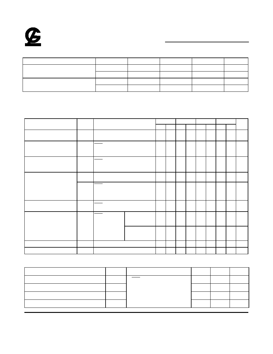
Pin Descriptions:
Name
Function
A
0
≠ A
15
Address Inputs
CE
1
and CE
2
Chip Enable Input
OE
Output Enable Input
WE
Write Enable Input
I/O
0
≠ I/O
15
Data Input and Data Output
V
CC
3V Power Supply
GND
Ground
NC
No Connection
Truth Table:
CE OE WE BLE BHE
I/O0-I/O7
I/O8-I/O15
Power
Mode
H
X
X
X
X
High-Z
High-Z
Standby
Standby
L
L
H
L
H
Data Out
High-Z
Active
Low byte Read
L
L
H
H
L
High-Z
Data Out
Active
High Byte Read
L
L
H
L
L
Data Out
Data Out
Active
Word Read
L
X
L
L
L
Data In
Data In
Active
Word Write
L
X
L
L
H
Data In
High-Z
Active
Low Byte Write
L
X
L
H
L
High-Z
Data In
Active
High byte Write
L
H
H
X
X
High-Z
High-Z
Active
Output Disable
L
X
X
H
H
High-Z
High-Z
Active
Output Disable
Absolute Maximum Ratings*
Parameter
Symbol
Minimum
Maximum
Unit
Voltage on Any Pin Relative to Gnd
Vt
-0.5
4.6
V
Power Dissipation
P
T
-
1.0
W
Storage Temperature (Plastic)
Tstg
-55
+150
∞
C
Temperature Under Bias
Tbias
-40
+85
∞
C
*Note : Stresses greater than those listed above Absolute Maximum Ratings may cause permanent damage to the device.
This is a stress rating only and functional operation of the device at these or any conditions outside those indicated
in the operational sections of this specification is not implied. Exposure to absolute maximum rating conditions for
extended periods may affect reliability.
G -LINK
GLT6100L16
Ultra Low Power 64k x 16 CMOS SRAM
May 2000(Rev. 0.3)
G-Link Technology Corporation
2701 Northwestern Parkway
Santa Clara, CA 95051, U.S.A.
G-Link Technology Corporation, Taiwan
6F No. 24-2, Industry E. RD. IV, Science Based
Industrial Park, Hsin Chu, Taiwan.
- 3 -
Recommended Operating Conditions ( TA = -25
∞
C to + 85
∞
C** )
Parameter
Symbol
Min
Typ
Max
Unit
V
CC
2.7
3.0
3.3
V
Supply Voltage
Gnd
0.0
0.0
0.0
V
V
IH
2.2
-
V
CC
+0.5
V
Input Voltage
V
IL
-0.5*
-
0.6
V
* V
IL
min = -2.0V for pulse width less than t
RC
/2.
** For Industrial Temperature.
DC Operating Characteristics
( Vcc=2.7 to 3.3V , T
A
=-25
∞
C to + 85
∞
C)
55
70
85
100
Parameter
Sym.
Test Conditions
Min Max Min Max Min Max Min Max
Unit
Input Leakage Current
I
LI
V
CC
= Max,
Vin = Gnd to V
CC
1
1
1
1
µ
A
Output Leakage
Current
I
LO
CE =V
IH
or V
CC
= Max,
V
OUT
= Gnd to V
CC
1
1
1
1
µ
A
Operating Power
Supply Current
I
CC
CE =V
IL
,V
IN
=V
IH
or V
IL
, I
OUT
=0
3
3
3
3
mA
I
CC1
I
OUT
= 0mA,
Min Cycle, 100% Duty
40
35
30
30
mA
Average Operating
Current
I
CC2
CE
0.2V
I
OUT
= 0mA,
Cycle Time=1
µ
s, 100% = Duty
3
3
3
3
mA
Standby Power Supply
Current(TTL Level)
I
SB
CE =V
IH
0.5
0.5
0.5
0.5
mA
GLT6100L16LL
5
5
5
5
µ
A
Standby Power Supply
Current (CMOS Level)
I
SB1
CE
V
CC
-0.2V
V
IN
0.2V or
V
IN
V
CC
-0.2V
GLT6100L16SL
1
1
1
1
µ
A
Output Low Voltage
V
OL
I
OL
= 2 mA
0.4
0.4
0.4
0.4
V
Output High Voltage
V
OH
I
OH
= -2 mA
2.4
2.4
2.4
2.4
V
Data Retention
Parameter
Sym.
Test Conditions
Min.
Max.
Unit
V
CC
for Data retention
V
DR
2.0
-
V
Data Retention Current
I
CCDR
1
µ
A
Chip Deselect to Data Retention Time
t
CDR
0
-
ns
Operating Recovery Time
(2)
t
R
CE
V
CC
-0.2V
V
IN
V
CC
-0.2V or
V
IN
0.2V
t
RC
-
ns
G -LINK
GLT6100L16
Ultra Low Power 64k x 16 CMOS SRAM
May 2000(Rev. 0.3)
G-Link Technology Corporation
2701 Northwestern Parkway
Santa Clara, CA 95051, U.S.A.
G-Link Technology Corporation, Taiwan
6F No. 24-2, Industry E. RD. IV, Science Based
Industrial Park, Hsin Chu, Taiwan.
- 4 -
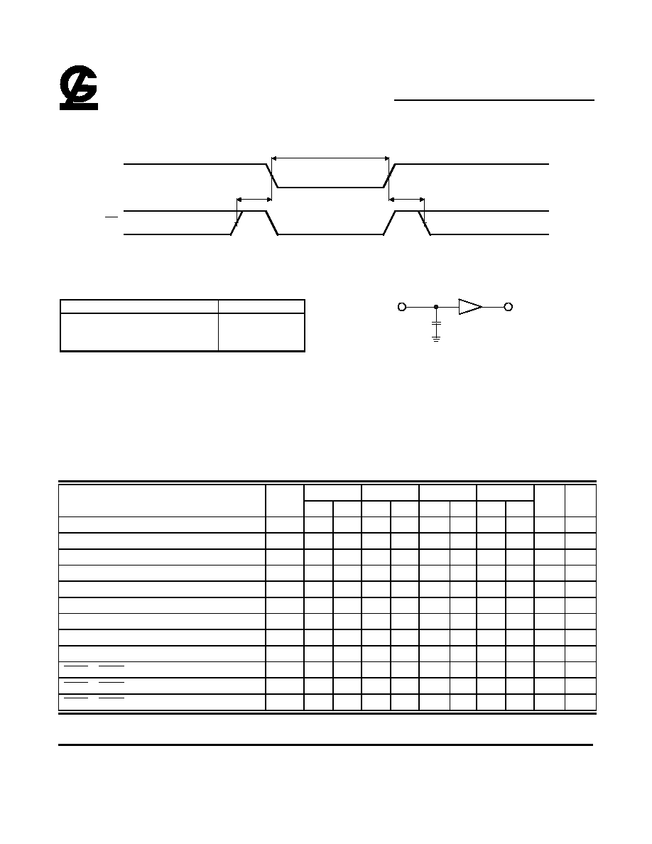
Data Retention Waveform
(TA = -25
∞
C to + 85
∞
C)
Data Retention Mode
Vcc
CE
V
DR
V
DR >= 2.0V
t
R
t
CDR
Vcc_typ
Vcc_typ
V
IH
V
IH
AC Test Conditions
AC Test Loads and Waveforms
C
L
*
TTL
Output Load Condition
*Including Scope and Jig Capacitance
55ns / 70ns / 85ns
C
L
= 30pf + 1TTL Load
Load 100ns
C
L
= 100pf + 1TTL Load
Read Cycle
(9)
( Vcc=2.7V to 3.3V, T
A
= -25
∞
C to + 85
∞
C)
55
70
85
100
Parameter
Symbol
Min
Max
Min
Max
Min
Max
Min
Max
Unit
Note
Read Cycle Time
t
RC
55
70
85
100
ns
Address Access Time
t
AA
55
70
85
100
ns
Chip Enable Access Time
t
ACE
55
70
85
100
ns
Output Enable Access Time
t
OE
35
40
40
50
ns
Output Hold from address Change
t
OH
10
10
10
10
ns
Chip Enable to Output in Low-Z
t
LZ
10
10
10
10
ns
4,5
Chip Disable to Output in High-Z
t
HZ
25
30
35
40
ns
3,4,5
Output Enable to Output in Low-Z
t
OLZ
5
5
5
5
ns
Output Disable to Output in High-Z
t
OHZ
25
25
30
35
ns
BLE , BHE Enable to Output in Low-Z
t
BLZ
5
5
5
5
ns
4,5
BLE , BHE Disable to Output in High-Z
t
BHZ
25
25
30
35
ns
3,4,5
BLE , BHE Access Time
t
BA
35
40
40
50
ns
Input Pulse Levels
0.6V to 2.2V
Input Rise and Fall Time
Input and Output Timing
Reference Level
5 ns
1.4V
G -LINK
GLT6100L16
Ultra Low Power 64k x 16 CMOS SRAM
May 2000(Rev. 0.3)
G-Link Technology Corporation
2701 Northwestern Parkway
Santa Clara, CA 95051, U.S.A.
G-Link Technology Corporation, Taiwan
6F No. 24-2, Industry E. RD. IV, Science Based
Industrial Park, Hsin Chu, Taiwan.
- 5 -
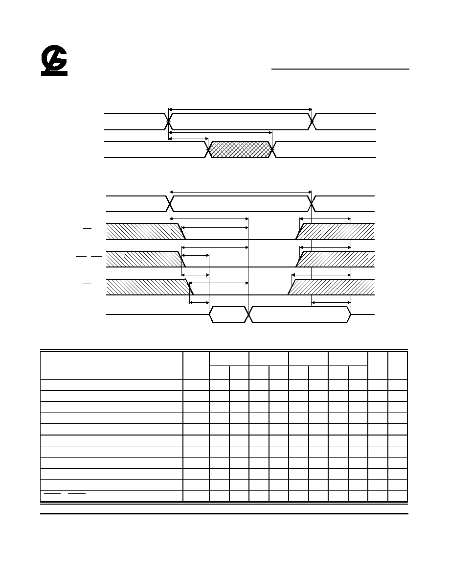
Timing Waveform of Read Cycle 1 (Address Controlled)
D
OUT
t
RC
Address
t
OH
t
AA
Previous Data Valid
Data Valid
Timing Waveform of Read Cycle 2
(14~16)
D
OUT
t
RC
Address
t
OH
t
AA
t
LZ
t
OE
t
BA
t
OLZ
t
BLZ
t
HZ
t
BHZ
t
OHZ
t
OH
Data Valid
High - Z
CE
BLE / BHE
OE
Write Cycle
(11)
( Vcc=2.7V to 3.3V, T
A
= -25
∞
C to + 85
∞
C)
55
70
85
100
Parameter
Symbol
Min Max Min Max Min Max Min Max
Unit Note
Write Cycle Time
t
WC
55
70
85
100
ns
Chip Enable to Write End
t
CW
50
60
70
80
ns
Address Setup to Write End
t
AW
50
60
70
80
ns
Address Setup Time
t
AS
0
0
0
0
ns
Write Pulse Width
t
WP
45
50
60
70
ns
Write Recovery Time
t
WR
0
0
0
0
ns
Data Valid to Write End
t
DW
25
30
35
40
ns
Data Hold Time
t
DH
0
0
0
0
ns
Write Enable to Output in High-Z
t
WHZ
25
30
35
40
ns
Output Active from Write End
t
OW
5
5
5
5
ns
BLE , BHE Setup to Write End
t
BW
50
60
70
80
ns