 | –≠–ª–µ–∫—Ç—Ä–æ–Ω–Ω—ã–π –∫–æ–º–ø–æ–Ω–µ–Ω—Ç: G1201 | –°–∫–∞—á–∞—Ç—å:  PDF PDF  ZIP ZIP |

Ver 1.1
Mar 15, 2002
TEL: 886-3-5788833
http://www.gmt.com.tw
1
G1201
Global Mixed-mode Technology Inc.
Rail-to-Rail I/O, 100mA Output Single-Supply Amplifiers
Features
Single-Supply Operation: 2.2 Volts to 6 Volts
High Output Current: ±100mA
Wide Bandwidth: 3.5 MHz
Slew Rate: 6.2 V/µs
No Phase Reversal
Unity Gain Stable
Rail-to-Rail Input and Output
Applications
Multimedia Audio
LCD Driver
ASIC Input or Output Amplifier
Headphone Driver
General Description
The G1201 is dual rail-to-rail input and output sin-
gle-supply amplifiers featuring 100mA output drive
current. This high output current makes these amplifi-
ers excellent for driving either resistive or capacitive
loads. AC performance is very good with 3.5MHz
bandwidth, 6.2V/µs-slew rate and low distortion. All
are guaranteed to operate from a +3 volt single supply
as well as a +5 volt supply.
The very low input bias currents enable the G1201 to
be used for integrators and diode amplification and
other applications requiring low input bias current. Al-
lowing low current applications to control high current
loads.
Applications include audio amplification for computers,
sound ports, sound cards and set-top boxes. The
G1201 is very stable and capable of driving heavy
capacitive loads.
The ability to swing rail-to-rail at the inputs and outputs
enables designers to buffer CMOS ADC/DACs, ASICs
or other wide output swing devices in single-supply
systems.
Ordering Information
PART TEMP.
RANGE
PIN-PACKAGE
G1201
-40∞C to +85∞C
8 SOP
Pin Configuration
Rail-to-Rail is a registered trademark of Nippon Motorola, Ltd.
OUT B
OUT A
8
7
6
5
-IN A
+IN A
V-
V+
-IN B
+IN B
G1201
1
4
2
3
8Pin SOP
Ver 1.1
Mar 15, 2002
TEL: 886-3-5788833
http://www.gmt.com.tw
2
G1201
Global Mixed-mode Technology Inc.
Absolute Maximum Ratings*
Supply Voltage (V
S
).........................................+7V
Input Voltage ........................................GND to V
S
Differential Input Voltage**...............................±6V
Storage Temperature Range.............-65∞C to +150∞C
Operating Temperature Range............-40∞C to +85∞C
Junction Temperature Range............-65∞C to +150∞C
Lead Temperature Range (Soldering,60 sec)...+300∞C
JA
1
.........................................................150∞C/W
JC.............................................................................................
43∞C/W
1
JA
is specified for the worst case conditions,
JA
is specified for
device soldered onto a circuit board for surface-mount packages.
*Stresses above those listed under Absolute Maximum Ratings may cause permanent damage to the device. This is a stress rating
only; the functional operation of the device at these or any other conditions above those indicated in the operational sections of this
specification is not implied. Exposure to absolute maximum rating conditions for extended periods may affect device reliability.
**For supplies less than +6V, the differential input voltage is equal to
±
V
S
.
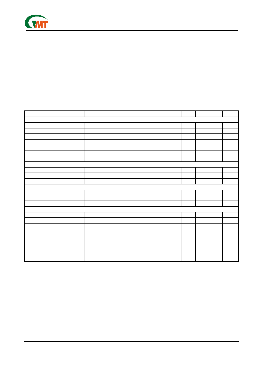
Electrical Characteristics
(V
S
= +3.0V, V
CM
= 1.5V, T
A
=+25∞C unless otherwise noted)
PARAMETER SYMBOL
CONDITIONS
MIN
TYP
MAX
UNIT
Input Characteristics
Offset Voltage
V
OS
5 15 mV
Input Bias Current
I
B
50
250
pA
Input Offset Current
I
OS
25
125 pA
Input Voltage Range
V
CM
0 3 V
Common-Mode Rejection Ratio
CMRR
V
CM
= 0V to 3V
60
dB
Large Signal Voltage Gain
A
VO
R
L
= 2k
V
O
= 0.5V to 2.5V
80 dB
Output Characteristics
Output Voltage High
V
OH
I
L
= 10mA
2.85
2.91
V
Output Voltage Low
V
OL
I
L
= 10mA
60
100
mV
Output Current
I
OUT
±100 mA
Power Supply
Power Supply Rejection Ratio
PSRR
f
i
= 1k
V
ripple(PEAK)
= 1V
63 dB
Supply Current/Amplifier
I
SY
V
O
= 0V
1.5
2.5
mA
Dynamic Performance
Slew Rate
SR
R
L
= 2k
2.8 V/µs
Settling Time
t
s
To
0.1%
2.5 µs
Gain
Bandwidth
Product
GBP
2.2 MHz
Channel Separation
CS
f = 1kHz
R
L
= 32
70 dB
Total Harmonic Distortion
THD
f = 1kHz
A
V
= -1
R
L
=32
V
O(P-)
=2.45V
50
dB
Specifications subject to change without notice.

Ver 1.1
Mar 15, 2002
TEL: 886-3-5788833
http://www.gmt.com.tw
3
G1201
Global Mixed-mode Technology Inc.
Electrical Characteristics
(V
S
= +5.0V, V
CM
= 2.5V, T
A
=+25∞C unless otherwise noted)
PARAMETER SYMBOL
CONDITIONS
MIN
TYP
MAX
UNIT
Input Characteristics
Offset Voltage
V
OS
5 15 mV
Input Bias Current
I
B
50
500
pA
Input Offset Current
I
OS
25
250 pA
Input Voltage Range
V
CM
0 5 V
Common-Mode Rejection Ratio
CMRR
V
CM
= 0V to 5V
40
65
dB
Large Signal Voltage Gain
A
VO
R
L
= 2k
V
O
= 0.5V to 4.5V
70 90 dB
Output Characteristics
Output Voltage High
V
OH
I
L
= 10mA
4.90
4.94
V
Output Voltage Low
V
OL
I
L
= 10mA
50
100
mV
Output Current
I
OUT
±100 mA
Power Supply
Power Supply Rejection Ratio
PSRR
f
i
= 1kHz
V
ripple(PEAK)
= 1V
50 66 dB
Supply Current/Amplifier
I
SY
V
O
= 0V
3.5
6
mA
Dynamic Performance
Slew Rate
SR
R
L
= 2k
6.2 V/
µs
Full-Power Bandwidth
BW
p
R
L
= 32
V
O(P-P)
= 4.2V
THD = 50dB
30 kHz
Settling Time
t
s
To 0.1%
1.3
µs
Gain Bandwidth Product
GBP
3.5
MHz
Channel Separation
CS
f = 1kHz, R
L
= 32
70 dB
Total Harmonic Distortion
THD
f = 1kHz, A
V
= -1 R
L
= 32
, V
O(P-P)
=
4.3V 50 dB
Specifications subject to change without notice.
Caution
ESD (electrostatic discharge) sensitive device. Elec-
trostatic charges as high as 2000V readily accumulate
on the human body and test equipment and can dis-
charge without detection.
Although the G1201 feature proprietary ESD protec-
tion circuitry, permanent damage may occur on de-
vices subjected to high-energy electrostatic dis-
charges. Therefore, proper ESD precautions are rec-
ommended to avoid performance degradation or loss of
functionality.
Applications
Theory of Operation
The G1201 is an all-CMOS, high output current drive,
rail-to-rail input/output operational amplifier. Its high
output current drive and stability with heavy capacitive
loads makes the G1201 an excellent choice as a drive
amplifier.
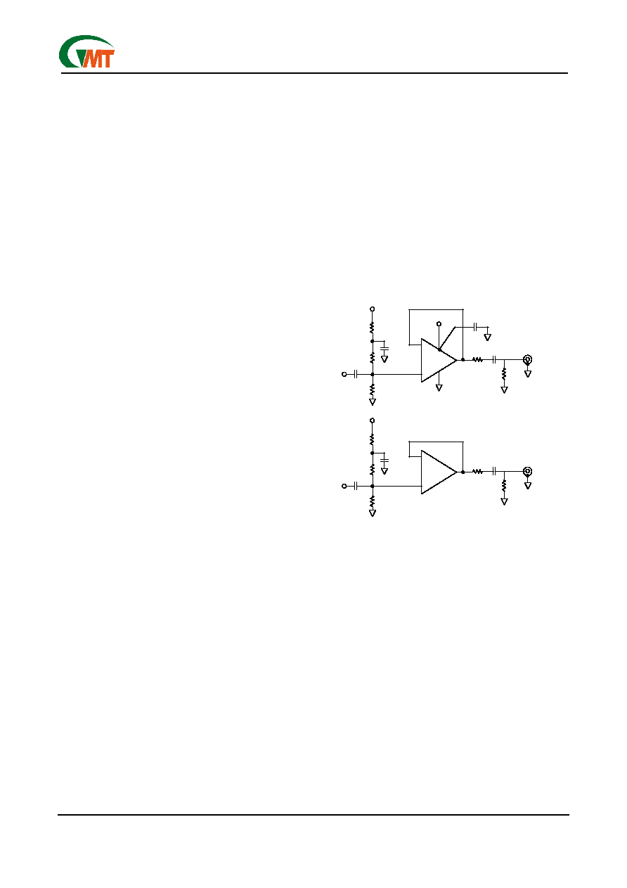
Short-Circuit Protection
As a result of the design of the output stage for maxi-
mum load current capability, the G1201 does not have
any internal short-circuit protection circuitry. Direct
connection of the G1201's output to the positive sup-
ply in single-supply applications will destroy the device.
In those applications where some protection is needed,
but not at the expense of reduced output voltage
headroom, a low value resistor in series with the out-
put, as shown in Figure 1, can be used. The resistor,
connected within the feedback loop of the amplifier,
will have very little effect on the performance of the
amplifier other than limiting the maximum available
output voltage swing.
Figure 1. Output Short-Circuit Protection
V
IN
+
_
+5V
R
X
20
V
OUT
Ver 1.1
Mar 15, 2002
TEL: 886-3-5788833
http://www.gmt.com.tw
4
G1201
Global Mixed-mode Technology Inc.
Input Overvoltage Protection
As with any semiconductor device, whenever the con-
dition exists for the input to exceed either supply volt-
age, the device's input overvoltage characteristic must
be considered. When an overvoltage occurs, the am-
plifier could be damaged depending on the magnitude
of the applied voltage and the magnitude of the fault
current. Although not shown here, when the input
voltage exceeds either supply by more than 0.6V,
pn-junctions internal to the G1201 energize allowing
current to flow from the input to the supplies. the
G1201 does not have any internal current limiting re-
sistors, so fault currents can quickly rise to damaging
levels.
This input current is not inherently damaging to the
device as long a it is limited to 5 mA or less. For the
G1201, once the input voltage exceeds the supply by
more than 0.6V the input current quickly exceeds 5
mA. If this condition continues to exist, an external
series resistor should be added. The size of the resis-
tor is calculated by dividing the maximum overvoltage
by 5 mA. For example, if the input voltage could reach
10V, the external resistor should be (10V/ 5mA) = 2k
.
This resistance should be placed in series with either
or both inputs if they are exposed to an overvoltage
condition.
A Single-Supply Headphone Amplifier
Because of its speed and large output drive, the
G1201 make an excellent headphone driver, as illus-
trated in Figure 2. Its low supply operation and
rail-to-rail inputs and outputs give a maximum signal
swing on a single +5V supply. To ensure maximum
signal swing available to drive the headphone, the
amplifier inputs are biased to V+/2, which in this case
is 2.5V. The 100k
resistor to the positive supply is
equally split into two 50 k
resistors, with their com-
mon point bypassed by 10µF to prevent power supply
noise from contaminating the audio signal.
The audio signal is then ac-coupled to each input
through a 10µF capacitor. A large value is needed to
ensure that the 20Hz audio information is not blocked.
If the input already has the proper dc bias, the ac cou-
pling and biasing resistors are not required. A 270µF
capacitor is used at the output to couple the amplifier
to the headphone. This value is much larger than that
used for the input because of the low impedance of
the head-phones, which can range from 32
to 600.
An additional 16
resistor is used in series with the
output capacitor to protect the op amp's output stage
by limiting capacitor discharge current. When driving a
32
load, the circuit exhibits less than 0.3% THD+N at
output drive levels of 4.2 V
P-P
.
Figure 2. A Single-Supply, Stereo Headphone Driver
+
1/2
G1201
_
+
LEFT
INPUT
50k
+
10µF
10µF
100k
50k
+V + 5V
+V + 5V
1µF 0.1 µF
16
+
270µF
50k
LEFT
HEADPHONE
+
1/2
G1201
_
+
RIGHT
INPUT
50k
+
10µF
10µF
100k
50k
+V
16
+
270µF
50k
RIGHT
HEADPHONE

Ver 1.1
Mar 15, 2002
TEL: 886-3-5788833
http://www.gmt.com.tw
5
G1201
Global Mixed-mode Technology Inc.
Input Common Mode Voltage Range Figure
Test Condition
T
A
= 25∞C, A
V
=1
V+ = 5V, V- = 0V, RL = 2K
V+ = 5V, V- = 0V, RL = 250
V+ = 3V, V- = 0V, RL = 2K
V+ = 3V, V- = 0V, RL = 250