 | –≠–ª–µ–∫—Ç—Ä–æ–Ω–Ω—ã–π –∫–æ–º–ø–æ–Ω–µ–Ω—Ç: G5103 | –°–∫–∞—á–∞—Ç—å:  PDF PDF  ZIP ZIP |
Ver: 1.1
Sep 20, 2004
TEL: 886-3-5788833
http://www.gmt.com.tw
1
G5103
Global Mixed-mode Technology Inc.
Micro-power Step-Up DC/DC Converters in SOT-23-5
Features
Configurable Output Voltage Up to 16V
20µA Quiescent Current
<1µA Shutdown Current
<1µA Shutdown Pin Current
Supply Range from 2.5V to 6.5V
Low V
DS(on)
: 250mV (I
SW
=300mA)
Tiny SOT-23-5 Package
Applications
STN/TFT LCD Bias
Personal Digital Assistants (PDAs)
Handheld Computers
Digital Still Cameras
Cellular Phones
WebPad
White LED Driver
Local 3V to 5V Conversion
General Description
The G5103 boost converter is designed for small/ me-
dium size LCD panel of high bias voltage.
Due to a typical 20µA quiescent current and 2.5V~
6.5V supply voltage range, it is suitable for battery
powered portable applications. Such as PDAs and
Handheld Computers. When the IC sets to shutdown
mode, it only consumes less than 1µA.
Furthermore, the 350mA current limit, 500ns fixed
minimum off-time and tiny SOT23-5 package facilitates
the use of smaller inductor and other surface-mount
components to minimize the PCB size in those
space-conscious applications.
To control the IC, no other external current is needed
for the shutdown pin. It typically consumes less than
1µA of full supply range.
Ordering Information
ORDER
NUMBER
ORDER NUMBER
(Pb Free)
MARKING TEMP.
RANGE PACKAGE
G5103T11U
G5103T11Uf
5103x
-40∞C ~ +85∞C
SOT-23-5
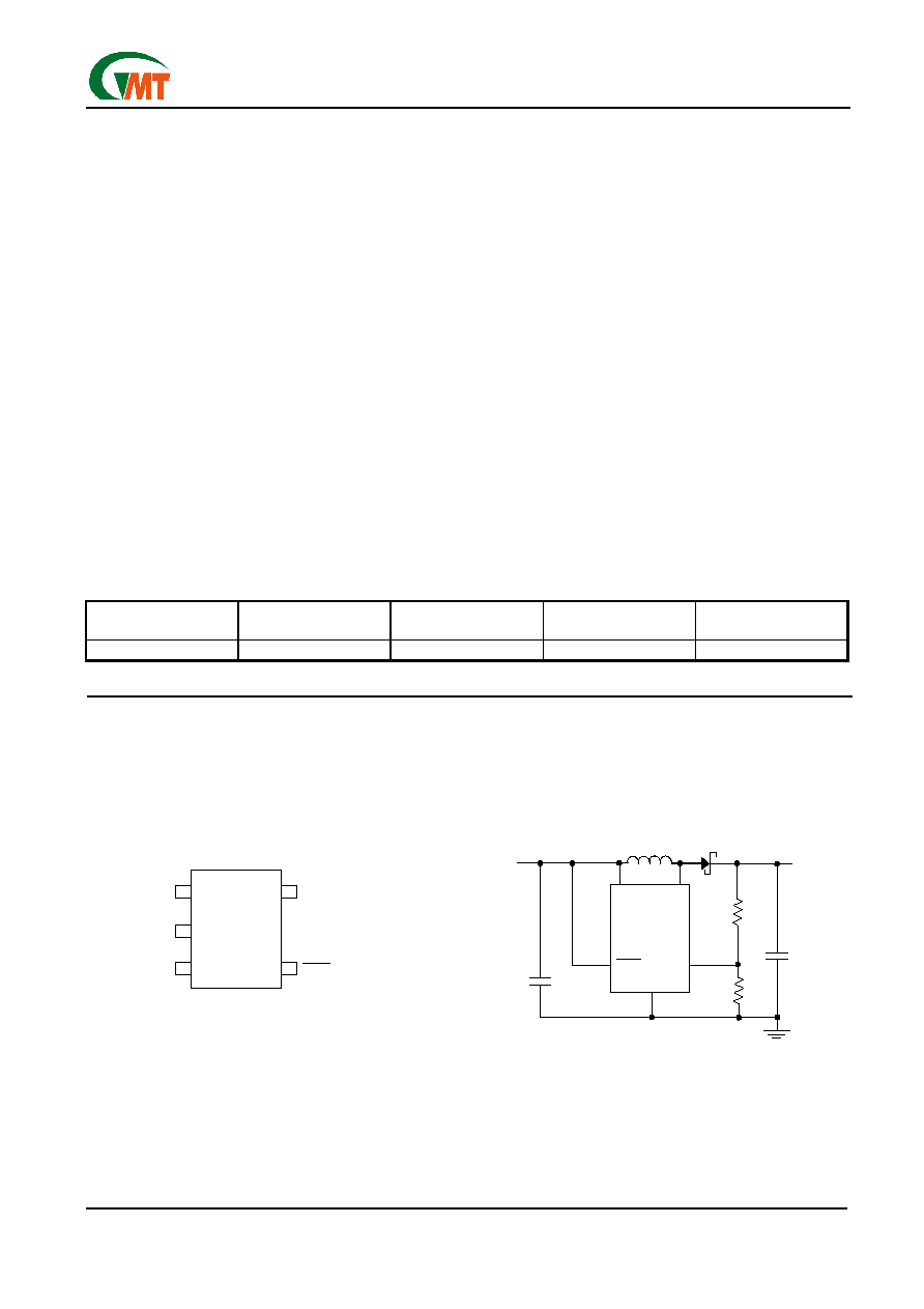
Pin Configuration
Typical Application Circuit
G963
VCC
SHDN
SOT-23-5
G5103
5
4
1
SW
2
3
GND
FB
VCC
SW
SHDN
FB
GND
G5103
1µF
4.7µF
10µH
80.6k
V
IN
2.5V to 4.2V
1M
16V
12mA
G963
VCC
SHDN
SOT-23-5
G5103
5
4
1
SW
2
3
GND
FB
VCC
SW
SHDN
FB
GND
G5103
1µF
4.7µF
10µH
80.6k
V
IN
2.5V to 4.2V
1M
16V
12mA

Ver: 1.1
Sep 20, 2004
TEL: 886-3-5788833
http://www.gmt.com.tw
2
G5103
Global Mixed-mode Technology Inc.
Absolute Maximum Ratings
SW to GND.........................................-0.3V to +18V
FB to GND............... .............................-0.3V to V
CC
VCC,
SHDN
to
GND....................................-0.3V to +7V
Operating Temperature Range (Note 1)..-40∞C to +85∞C
Junction Temperature .......................................+125∞C
Storage Temperature.........................-65∞C to +150∞C
Reflow Temperature (soldering, 10sec)..............260∞C
Stress beyond those listed under "Absolute Maximum Rating" may cause permanent damage to the device.
Electrical Characteristics
(V
CC
= 3.6V,
V
SHDN
= 3.6V, T
A
=
25∞C
)
PARAMETER CONDITIONS
MIN
TYP
MAX
UNITS
Input Voltage Range
2.5
6.5
V
Not Switching
20
35
µA
Quiescent Current
V
SHDN
= 0V
0.1 1 µA
FB Comparator Trip Point
1.18
1.2
1.22
V
Output Voltage Line Regulation
2.5V<V
IN
<6.5V
-0.05
%/V
FB Pin Bias Current (Note 2)
V
FB
= 1.2V
30
80
nA
V
FB
> 1V
500
ns
Switch Off Time
V
FB
< 0.6V
1.6
µs
Switch V
DS(ON)
I
SW
= 300mA
250
350
mV
Switch Current Limit
300
350
400
mA
SHDN
Pin Current
0.1
1
µA
SHDN
Input Voltage High
0.9
V
SHDN
Input Voltage Low
0.25
V
Switch Leakage Current
Switch Off, V
SW
= 16V
0.01
5
µA
Note 1: The G5103 are guaranteed to meet performance specifications from 0∞C to 85∞C. Specifications over the
-40∞C to 85∞C operating temperature range are assured by design, characterization and correlation with
statistical process controls.
Note 2: Bias current flows into the FB pin.
Block Diagram
+
+
VREF
BIAS
SHUTDOWN
LOGIC
C2
SW
L1
SHDN
VCC
C1
R1
R2
VOUT
FB
ERROR
COMP
1.2V
en_sw
GND
PUMP CONTROL
OC
COMP
DRIVER
T
OFF
PULSE
CONTROL
V
OUT
V
IN
+
+
VREF
BIAS
SHUTDOWN
LOGIC
C2
SW
L1
SHDN
VCC
C1
R1
R2
VOUT
FB
ERROR
COMP
1.2V
en_sw
GND
PUMP CONTROL
OC
COMP
DRIVER
T
OFF
PULSE
CONTROL
V
OUT
V
IN
Ver: 1.1
Sep 20, 2004
TEL: 886-3-5788833
http://www.gmt.com.tw
3
G5103
Global Mixed-mode Technology Inc.
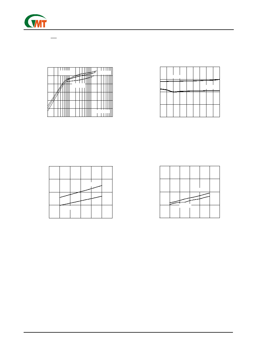
Typical Performance Characteristics
(V
CC
=+3.6V, V
SHDN
=+3.6V, L=10µH, T
A
=25∞C, unless otherwise noted.)
Output Voltage vs. Load Current
15
15.5
16
16.5
17
1
2
3
4
5
6
7
8
9
10
Load Current (mA)
Output Voltage (V)
V
IN
=2.7V
V
IN
=4.2V
Efficiency vs. Load Current
30
40
50
60
70
80
90
0.1
1
10
100
Load Current (mA)
Efficiency (%)
V
IN
=4.2V
V
IN
=3.6V
V
IN
=2.7V
VOUT=16V
Vds_on vs. Temperature
100
200
300
400
500
-20
0
20
40
60
80
100
Temperature (∞C)
Switch Vds_on (mV)
V
IN
=2.7V
V
IN
=4.2V
Quiescent Current vs. Temperature
10
20
30
40
50
-20
0
20
40
60
80
100
Temperature (∞C)
Quiescent Current (µA)
V
IN
=2.7V
V
IN
=4.2V
Ver: 1.1
Sep 20, 2004
TEL: 886-3-5788833
http://www.gmt.com.tw
4
G5103
Global Mixed-mode Technology Inc.
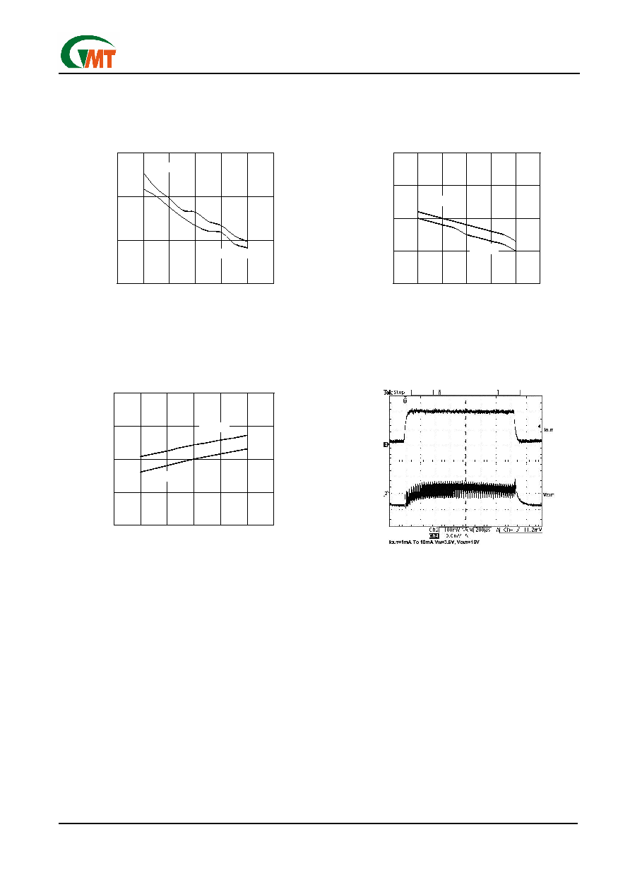
Typical Performance Characteristics
(Continued)
Feedback Voltage vs. Temperature
1.18
1.19
1.2
1.21
1.22
-20
0
20
40
60
80
100
Temperature (∞C)
Feedback Voltage (V)
V
IN
=2.7V
V
IN
=4.2V
FB Bias Current vs. Temperature
15
20
25
30
-20
0
20
40
60
80
100
Temperature (∞C)
Feedback Bias Current (nA)
V
IN
=2.7V
V
IN
=4.2V
Switch Current Limit vs. Temperature
250
300
350
400
450
-20
0
20
40
60
80
100
Temperature (∞C)
Peak Current
(mA)
V
IN
=2.7V
V
IN
=4.2V
Load Transient

Ver: 1.1
Sep 20, 2004
TEL: 886-3-5788833
http://www.gmt.com.tw
5
G5103
Global Mixed-mode Technology Inc.
Pin Description
PIN NAME
FUNCTION
1
SW
Switch Pin. The drain of the internal NMOS power switch. Connect this pin to inductor.
2 GND
Ground.
3 FB
Feedback Pin. Set the output voltage by selecting values for R1 and R2 (see Block Diagram):
R1 = R2
2
.
1
V
OUT
-1
4
SHDN
Active-Low Shutdown Pin. Tie this pin to logic-high to enable the device or tied it to logic-low to turn this
device off.
5
VCC
Input Supply Pin. Bypass this pin with a capacitor as close to the device as possible.
Function Description
The G5103 is a boost converter with a NMOS
switch embedded (refer to Block Diagram). The
boost cycle is getting started when FB pin voltage
drop below 1.2V as the NMOS switch turns on.
During the switch on period, the inductor current
ramps up until 350mA current limit is reached. Then
turns the switch off, while the inductor current flows
through external schottky diode, and ramps down to
zero. During the switch off period, the inductor cur-
rent charges output capacitor and the output volt-
age is boosted up. This pumping mechanism con-
tinues cycle by cycle until the FB pin voltage ex-
ceed 1.2V and entering the none switching mode.
In this mode, the G5103 consumes as low as 20uA
typically to save battery power.
Applications Information
Choosing an Inductor
There are several recommended inductors that work
well with the G5103 in Table 1. Use the equations and
recommendations in the next few sections to find the
proper inductance value for your design.
Table 1. Recommended Inductors
PART VALUE
(µH) MAX DCR () VENDOR
LQH3C4R7
LQH3C100
LQH3C220
4.7
10
22
0.26
0.30
0.92
Murata
www.murata.com
CD43-4R7
CD43-100
CDRH4D18-4R
7
CDRH4D18-100
4.7
10
4.7
10
0.11
0.18
0.16
0.20
Sumida
www.sumida.com
DO1608-472
DO1608-103
DO1608-223
4.7
10
22
0.09
0.16
0.37
Coilcraft
www.coilcraft.com
Inductor Selection--Boost Regulator
The appropriate inductance value for the boost regu-
lator application may be calculated from the following
equation. Select a standard inductor close to this
value.
V
OUT
-V
IN(MIN)
+V
D
L =
I
LIM
x t
OFF
Where V
D
= 0.4V (Schottky diode voltage), I
LIM
=
350mA and t
OFF
= 500ns. A larger value can be used
to lightly increase the available output current, but limit
it to about twice the calculating value. When too large
of an inductor will increase the output voltage ripple
without providing much additional output current. In
varying V
IN
condition such as battery power applica-
tions, use the minimum V
IN
value in the above equa-
tion. A smaller value can be used to give smaller
physical size, but the inductor current overshoot will be
occurs (see Current Limit Overshoot section).
Inductor Selection--SEPIC Regulator
For a SEPIC regulator using the G5103, the approxi-
mate inductance value can be calculated by below
formula. As for the boost inductor selection, a larger or
smaller value can be used.
V
OUT
+ V
D
L = 2
I
LIM
x t
OFF
Current Limit Overshoot
The G5103 use a constant off-time control scheme,
the power switch is turned off after the 350mA current
limit is reached. When the current limit is reached and
when the switch actually turns off, there is a 100ns
delay time. During this time, the inductor current ex-
ceeds the current limit by a small amount. The formula
below can calculate the peak inductor current.
V
IN(MAX)
- V
SAT
I
PEAK
= I
LIM
+
L
x 100ns
Where V
SAT
= 0.25V (switch saturation voltage). When
the systems with high input voltages and uses smaller
inductance value, the current overshoot will be most
apparent. This overshoot can be useful as it helps in-
crease the amount of available output current. To use
small inductance value for systems design, the current
limit overshoot can be quite high. Even if it is internally
current limited to 350mA, the power switch of the
G5103 can operate larger currents without any prob-
lem, but the total efficiency will suffer. The I
PEAK
is keep
below 500mA for the G5103 will be obtained best per-
formance.