 | –≠–ª–µ–∫—Ç—Ä–æ–Ω–Ω—ã–π –∫–æ–º–ø–æ–Ω–µ–Ω—Ç: G571 | –°–∫–∞—á–∞—Ç—å:  PDF PDF  ZIP ZIP |
Ver 1.1
Jan 08, 2001
TEL: 886-3-5788833
http://www.gmt.com.tw
1
G571
Global Mixed-mode Technology Inc.
Single-Slot PCMCIA/CardBus Power Controllers
Features
Fully Integrated V
CC
and V
PP
Switching for Sin-
gle-Slot PC Card
TM
Interface
Low r
DS(on)
(180-m
5V V
CC
Switch and 3.3V V
CC
Switch)
Compatible With Controllers From Cirrus, Ri-
coh, O
2
Micro, Intel, and Texas Instruments
3.3V Low-Voltage Mode
Meets PC Card Standards
12V Supply Can Be Disabled Except During
12V Flash Programming
Short Circuit and Thermal Protection
Space-Saving 16 Pin SSOP
Compatible With 3.3V, 5V, and 12V PC Cards
Break-Before-Make Switching
Application
Notebook PC
Electronic Dictionary
Personal Digital Assistance
Digital still Camera
Description
The G571 PC Card power-interface switch provides an
integrated power-management solution for a single PC
Cards. All of the discrete power MOSFETs, a logic
section, current limiting, and thermal protection for PC
Card control are combined on a single integrated cir-
cuit. The circuit allows the distribution of 3.3V, 5V,
and/or 12V card power, and is compatible with many
PCMCIA controllers. The current-limiting feature
eliminates the need for fuses, which reduces compo-
nent count and improves reliability. Current-limit re-
porting can help the user isolate a system fault to the
PC Card.
The G571 features a 3.3V low voltage mode that al-
lows for 3.3V switching without the need for 5V. Bias
power can be derived from either the 3.3V or 5V inputs.
This facilitates low-power system designs such as
sleep mode and pager mode where only 3.3V is
available.
End equipment for the G571 includes notebook com-
puters, desktop computers, personal digital assistants
(PDAs), digital cameras and bar-code scanners.
Ordering Information
PART NUMBER TEMP. RANGE
PACKAGE
G571S1
-40∞C to +85∞C
16-SSOP
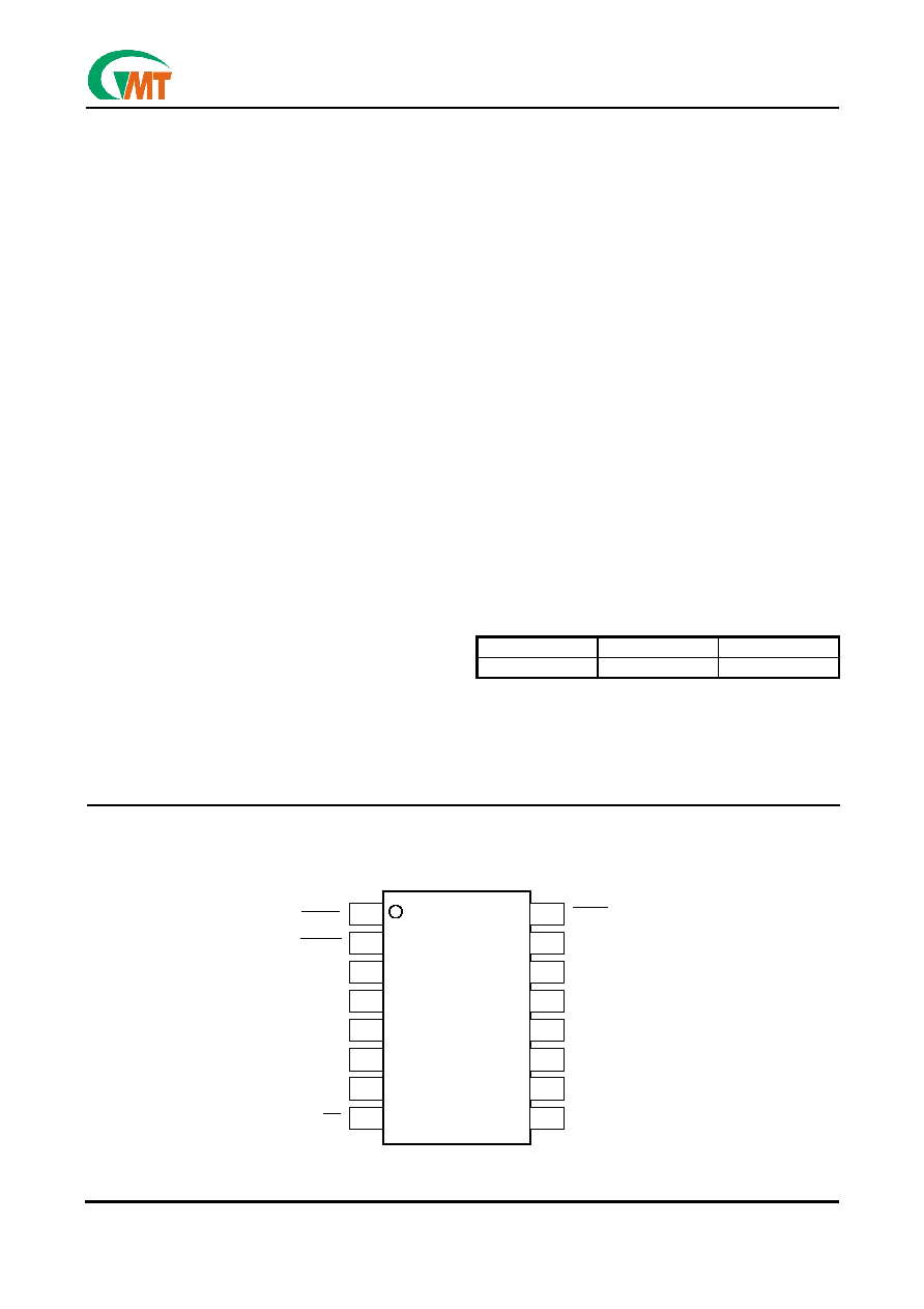
Pin Configuration
1
AVCC
AVCC
AVCC
AVPP
12V
3.3V
5V
5V
GND
OC
2
3
4
5
6
7
8
G571
VPPD0
16Pin SSOP
VCCD0
VCCD1
3.3V
SHDN
VPPD1
16
15
14
13
12
11
10
9
Ver 1.1
Jan 08, 2001
TEL: 886-3-5788833
http://www.gmt.com.tw
2
G571
Global Mixed-mode Technology Inc.
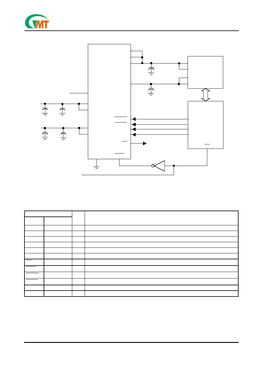
Typical PC-card Power-distribution application
Terminal Functions
TERMINAL
NAME NO.
I/O DESCRIPTION
3.3V 3,4
I
3.3V
V
CC
input for card power and/or chip power if 5V is not present
5V 5,6
I
5V
V
CC
input for card power and/or chip power
12V 9
I
12V
V
PP
input card power
AVCC
11,12,13
O
Switched output that delivers 0V,3.3V,5V, or high impedance to card
AVPP
10
O
Switched output that delivers 0V,3.3V,5V,12V or high impedance to card
GND 7
Ground
OC
8
O
Logic-level overcurrent reporting output that goes low when an overcurrent condition exists
SHDN
16
I
Logic input that shuts down the G571 and sets all power outputs to high-impedance state
0
VCCD
1
I
Logic input that controls voltage of AVCC(see control-logic table)
1
VCCD
2 I
Logic input that controls voltage of AVCC(see control-logic table)
VPPD0
15
I
Logic input that controls voltage of AVPP(see control-logic table)
VPPD1
14
I
Logic input that controls voltage of AVPP(see control-logic table)
0.1µF
AVCC
AVCC
AVCC
AVPP
OC
To CPU
V
CC1
V
CC2
PC Card
Connector
V
PP1
V
PP2
VCC_EN0
PCMCIA
Controller
CS
5V
3.3V
1µF
0.1µF
1µF
0.1µF
12V
5V
5V
3.3V
3.3V
GND
0.1µF
12V
VCC_EN1
VPP_EN0
VPP_EN1
VCCD0
VCCD1
VPPD1
VPPD0
SHDN
Shutdown Signal From CPU
G571

Ver 1.1
Jan 08, 2001
TEL: 886-3-5788833
http://www.gmt.com.tw
3
G571
Global Mixed-mode Technology Inc.
Absolute Maximum Ratings Over Operating
Free-Air Temperature
(unless other-wise noted)*
Input voltage range for card power:
V
I(5V)
............................................................-0.3V to 7V
V
I(3.3V)
........................................................ -0.3V to 7V
V
I(12V)
.........................................................-0.3V to 14V
Logic input voltage.........................................-0.3V to 7V
Output current (each card):I
O (VCC).
.........internally limited
I
O(VPP)
............internally limited
Operating virtual junction temperature range, T
J.
........................................................-40∞C to 150∞C
Operating free-air temperature range,.T
A
.....................................................................................
-40∞C to 85∞C
Storage temperature range, T
STG
.......................................................-55∞C to 150∞C
Lead temperature 1.6 mm (1/16 inch) from case for
10 seconds..................................................260∞C
*
Stresses beyond those listed under "absolute maximum ratings
"
may cause permanent damage to the device. These are stress
rating only, and functional operation of the device at these or any other conditions beyond those indicated under "recommended op-
erating conditions
"
is not implied. Exposure to absolute≠maximum-rated conditions for extended periods may affect device reliability.
Recommended Operating Conditions
MIN MAX UNIT
V
I(5V)
0
5.25
V
V
I(3.3V)
0
5.25
V
Input voltage, V
I
V
I(12V)
0
13.5
V
I
O(AVCC)
1.0
A
Output current
I
O(AVPP)
150
mA
Operating virtual junction temperature, T
J
-40
125
∞C
Electrical Characteristics
(T
A
=25∞C)
Power Switch
PARAMETER TEST
CONDITIONS*
MIN
TYP MAX UNIT
5V to AVCC
V
I(5V)
= 5V
130
180
3.3V to AVCC
V
I(5V)
= 5V, V
I(3.3V)
=3.3V
130
180
3.3V to AVCC
V
I(5V)
= 0V, V
I(3.3V)
=3.3V
130
180
m
5V to AVPP
T
J
= 25∞C
6
3.3V to AVPP
T
J
= 25∞C
6
Switch resistance
12V to AVPP
T
J
= 25∞C
6
V
O(AVPP)
Clamp low voltage
I
PP
at 10mA
0.8
V
V
O(AVCC)
Clamp low voltage
I
CC
at 10mA
0.8
V
I
PP
high-impedance State T
A
= 25∞C
1
10
I
IKG
Leakage current
I
CC
high-impedance State T
A
= 25∞C
1
10
µA
V
I(5V)
= 5V
V
O(AVCC)
=5V,V
O(AVPP)
=12V
75
150
V
I(5V)
= 0V, V
I(3.3V)
= 3.3V
V
O(AVCC)
=3.3V,V
O(AVPP)
= 12V
75
150
I
I
Input current
Shutdown mode
V
O(AVCC)
=V
O(AVPP)
= Hi-Z
1
3
µA
I
O(AVCC)
0.8
2.2
A
I
OS
Short-circuit Output-
current Limit
I
O(AVPP)
output powered into a short to GND
120 400 mA
*Pulse-testing techniques maintain junction temperature close to ambient temperatures; thermal effects must be taken into account separately.

Ver 1.1
Jan 08, 2001
TEL: 886-3-5788833
http://www.gmt.com.tw
4
G571
Global Mixed-mode Technology Inc.
Logic Section
PARAMETER TEST
CONDITION*
MIN
MAX
UNIT
Logic input current
1
µA
Logic input high level
2
V
Logic input low level
0.8
V
V
I(5V)
= 5V, I
O
=1mA V
I(5V)
- 0.4
Logic output high level
V
I(5V)
=0V,I
O
= 1mA,V
I(3.3V)
= 3.3V
V
I(3.3V)
- 0.4
V
Logic output low level
I
O
= 1mA
0.4
V
*Pulse-testing techniques maintain junction temperature close to ambient temperatures; thermal effects must be taken into account separately.
Switching Characteristics **
PARAMETER TEST
CONDITION
MIN
TYP
MAX
UNIT
V
O (AVCC)
2.6
t
r
Rise times, output
V
O (AVPP)
10
V
O (AVCC)
7.5
t
f
Fall times, output
V
O (AVPP)
38
ms
t
on
14
V
I
(
VPPD0
) to V
O(AVPP)
t
off
44
t
on
3.2
V
I
(
1
VCCD
) to V
O(AVCC)
(3.3V)
t
off
17
t
on
4.4
t
pd
Propagation delay
(see Figure 1)
V
I
(
0
VCCD
) to V
O(AVCC)
(5V)
t
off
20
ms
**Switching Characteristics are with C
L
= 147µF.
ß Refer to Parameter Measurement Information
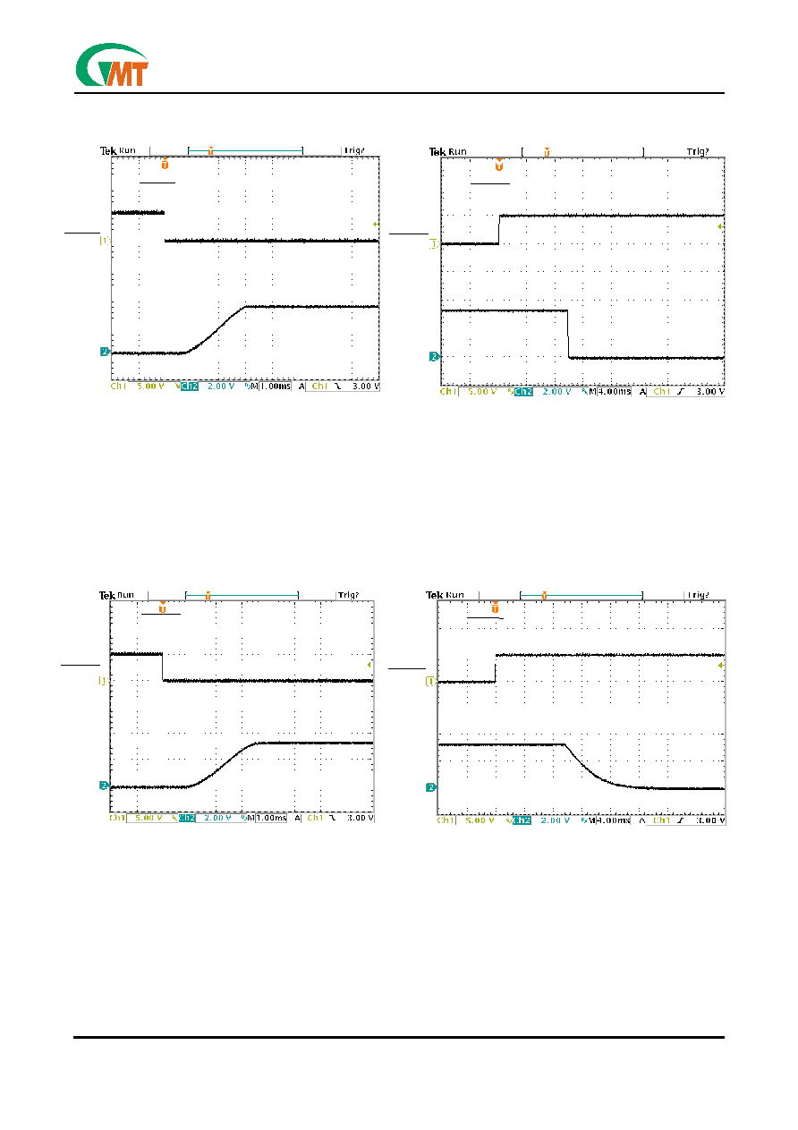
Parameter Measurement Information
Figure 1. Test Circuits and Voltage Waveforms
Table of Timing Diagrams
FIGURE
AVCC Propagation Delay and Rise Time With 1µF Load, 3.3V Switch
2
AVCC Propagation Delay and Fall Time With 1µF Load, 3.3V Switch
3
AVCC Propagation Delay and Rise Time With 147µF Load, 3.3V Switch
4
AVCC Propagation Delay and Fall Time With 147µF Load, 3.3V Switch
5
AVCC Propagation Delay and Rise Time With 1µF Load, 5V Switch
6
AVCC Propagation Delay and Fall Time With 1µF Load, 5V Switch
7
AVCC Propagation Delay and Rise Time With 147µF Load, 5V Switch
8
AVCC Propagation Delay and Fall Time With 147µF Load, 5V Switch
9
AVPP Propagation Delay and Rise Time With 1µF Load, 12V Switch
10
AVPP Propagation Delay and Fall Time With 1µF Load, 12V Switch
11
AVPP Propagation Delay and Rise Time With 147µF Load, 12V Switch
12
AVPP Propagation Delay and Fall Time With 147µF Load, 12V Switch
13
LOAD CIRCUIT
V
DD
GND
50%
90%
t
off
t
on
10%
V
I(12V)
GND
V
O(AVPP)
AVPP
C
L
VOLTAGE WAVEFORMS
50%
V
I(VPPD0)
(V
I(VPPD1)
=0V)
LOAD CIRCUIT
V
DD
GND
50%
90%
t
off
t
on
10%
V
I(3.3V)
GND
V
O(AVCC)
AVCC
C
L
VOLTAGE WAVEFORMS
V
I(VCCD1)
(V
I(VCCD0)
=V
DD
)
50%
Ver 1.1
Jan 08, 2001
TEL: 886-3-5788833
http://www.gmt.com.tw
5
G571
Global Mixed-mode Technology Inc.
Parameter Measurement Information
Figure 2. AVCC Propagation Delay and Rise
Time With 1µF Load, 3.3V Switch
Figure 3. AVCC Propagation Delay and Fall Time
With 1µF Load, 3.3V Switch
Figure 4. AVCC Propagation Delay and Rise Time
With 147µF Load, 3.3V Switch
Figure 5. AVCC Propagation Delay and Fall Time
With 147µF Load, 3.3V Switch
V C C D 0 =3.3 V
V C C D 1
AV C C
V C C D 0 = 3 .3 V
V C C D 1
AV C C
V C C D 0 = 3 .3V
V C C D 1
AV C C
V C C D 0=3.3V
V C C D 1
AV C C