Ver: 1.0
Jan 23, 2003
TEL: 886-3-5788833
http://www.gmt.com.tw
1
G574
Global Mixed-mode Technology Inc.
Dual-Slot PCMCIA/CardBus Power Controller
Features
Backward Compatible with G570
Fully Integrated V
CC
and V
pp
Switching for Dual
Slot PC Card
TM
Interface
3-Lead Serial Interface Compatible With
CardBus
TM
Controllers
3.3V Low Voltage Mode
Meets PC Card Standards
RESET for System Initialization of PC Cards
12V Supply Can Be Disabled Except During
12V Flash Programming
Short Circuit and Thermal Protection
30 Pin SSOP
Compatible With 3.3V, 5V and 12V PC Cards
Low R
DS(on)
(180-m
5V V
CC
Switch;
130 m
3.3V V
CC
Switch)
Break-Before-Make Switching
Internal power-On Reset
Standby mode: 60mA current limit (TYP)
Application
Notebook PC
Electronic Dictionary
POS
Description
The G574 PC Card power-interface switch provides an
integrated power-management solution for two PC Cards.
All of the discrete power MOSFETs, a logic section, cur-
rent limiting, and thermal protection for PC Card control
are combined on a single integrated circuit (IC). The cir-
cuit allows the distribution of 3.3V, 5V, and/or 12V card
power by means of the Serial interface. The current-
limiting feature eliminates the need for fuses, which re-
duces component count and improves reliability.
The G574 features a 3.3V low voltage mode that allows
for 3.3V switching without the need for 5V supply. This
facilitates low power system designs such as sleep
mode and pager mode where only 3.3V is available.
The G574 incorporates a reset function, selectable by
one of two inputs, to help alleviate system errors. The
reset function enables PC card initialization concurrent
with host platform initialization, allowing a system reset.
Reset is accomplished by grounding the V
CC
and V
PP
(flash-memory programming voltage) outputs, which
discharges residual card voltage.
This device also has the ability to program the xVpp
outputs independent of the xVCC outputs. A standby
mode that changes all output-current limits to 50mA
(typical) has been incorporated.
End equipment for the G574 includes notebook com-
puters, desktop computers, personal digital assistants
(PDAs), digital cameras and bar-code scanners
.
The G574 is backward-compatible with the G570.
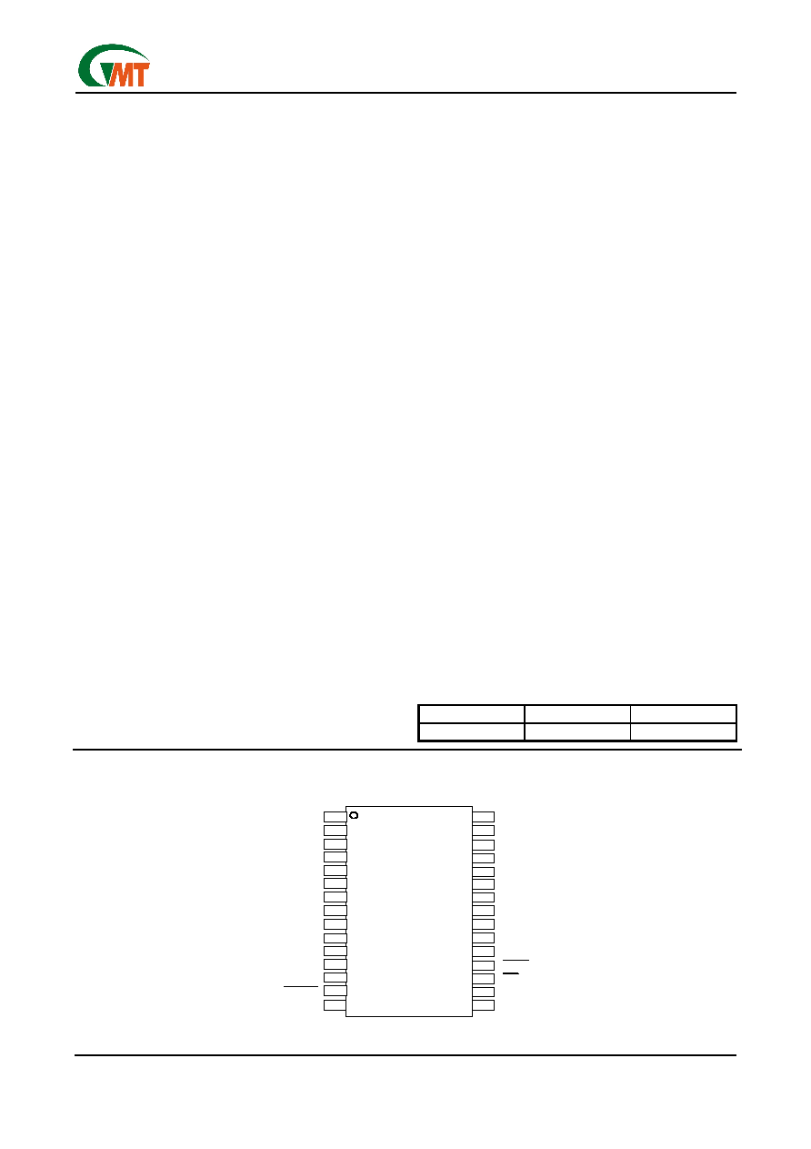
Ordering Information
PART NUMBER TEMP. RANGE
PACKAGE
G574SA
-40�C to +85�C
30 SSOP
Pin Configuration
M O D E
N C
N C
1 2V
B V P P
B V C C
B V C C
B V C C
S T B Y
O C
3 .3V
3 .3V
5 V
D A T A
C L O C K
L A T C H
R E S E T
1 2V
A V P P
A V C C
A V C C
A V C C
G N D
N C
R E S E T
3 .3V
G 574
5 V
30P in S S O P
5
6
7
8
9
1 0
1 1
1 2
1 3
1 4
2 6
2 7
2 8
2 5
2 4
2 3
2 2
2 1
2 0
1 9
1 8
1 7
1 6
1 5
1
4
3
2
5 V
3 0
2 9
N C
N C
Ver: 1.0
Jan 23, 2003
TEL: 886-3-5788833
http://www.gmt.com.tw
2
G574
Global Mixed-mode Technology Inc.
Absolute maximum ratings over operating
free-air temperature
(unless otherwise noted)*
Input voltage range for card power:
V
I(3.3V)
.......................................................-0.3V to 6V
V
I(5V)
........................................................-0.3V to 6V
V
I(12V).......
............................................... -0.3V to 14V
Logic input voltage......................................-0.3V to 6V
Output current (each card):
I
O (xVCC)..............
..................................internally limited
I
O(xVPP).
................................................ internally limited
Operating virtual junction temperature range, T
J
.......................................................-40�C to 125�C
Operating free-air temperature range, T
A
.......................................................-40�C to 85�C
Storage temperature range, T
STG
..........-55�C to 150�C
Thermal resistance
JA
SSOP 30.................................................122�C/W
Power dissipation P
D
(T
A
+25�C)
SSOP 30................................................1024mW
ESD...........................................................Note1
*Stresses beyond those listed under "absolute maximum ratings"may cause permanent damage to the device. These are stress rating
only, and functional operation of the device at these or any other conditions beyond those indicated under "recommended operating
conditions"is not implied. Exposure to absolute�maximum-rated conditions for extended periods may affect device reliability.
Note 1: ESD (electrostatic discharge) sensitive device. Proper ESD precautions are recommended to avoid performance degradation or
less of functionality.
Recommended Operating Conditions
Min Max Unit
V
I (5V)
2.7
5.25
V
V
I (3.3V)
2.7
5.25
V
Input voltage range, V
I
V
I (12V)
13.5
V
I
O (xVCC)
at 25�C
1
A
Output current
I
O (xVPP)
at 25�C
150
mA
Clock frequency
0 2.5
MHz
Operating virtual junction temperature, T
J
-40
125
�C
Typical PC Card Power-Distribution Application
0 .1 � F
0 .1 � F
1 2 V
1 2 V
A V C C
A V C C
A V C C
B V C C
B V C C
B V C C
A V P P
B V P P
D A T A
C L O C K
L A T C H
R E S E T
R E S E T
O C
S ys te m V o lta g e
S u p e rv is o r
o r
P C I B u s R e s e t
0 .1 � F
0 .1 � F
V
C C
V
C C
P C C a rd
C o n n e c to r A
V
P P 1
V
P P 2
P C C a rd
C o n n e c to r B
V
P P 2
V
P P 1
V
C C
V
C C
D A T A
C L O C K
L A T C H
P C M C IA
C o n tro lle r
5 V
3 .3 V
3 3 � F
0 .1 � F
3 3 � F
0 .1 � F
5 V
5 V
5 V
3 .3 V
3 .3 V
3 .3 V
G N D
G 5 7 4
0 .1 � F
1 0 � F
1 2 V
(C e ra m ic )
(C e ra m ic )
(C e ra m ic )
S T B Y
M O D E
G P I/O
0 .1 � F
0 .1 � F
1 2 V
1 2 V
A V C C
A V C C
A V C C
B V C C
B V C C
B V C C
A V P P
B V P P
D A T A
C L O C K
L A T C H
R E S E T
R E S E T
O C
S ys te m V o lta g e
S u p e rv is o r
o r
P C I B u s R e s e t
0 .1 � F
0 .1 � F
V
C C
V
C C
P C C a rd
C o n n e c to r A
V
P P 1
V
P P 2
P C C a rd
C o n n e c to r B
V
P P 2
V
P P 1
V
C C
V
C C
D A T A
C L O C K
L A T C H
P C M C IA
C o n tro lle r
5 V
3 .3 V
3 3 � F
0 .1 � F
3 3 � F
0 .1 � F
5 V
5 V
5 V
3 .3 V
3 .3 V
3 .3 V
G N D
G 5 7 4
0 .1 � F
1 0 � F
1 2 V
(C e ra m ic )
(C e ra m ic )
(C e ra m ic )
S T B Y
M O D E
G P I/O
Ver: 1.0
Jan 23, 2003
TEL: 886-3-5788833
http://www.gmt.com.tw
3
G574
Global Mixed-mode Technology Inc.
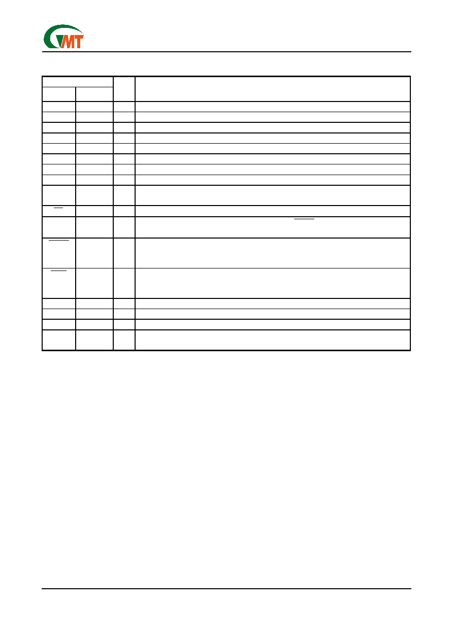
Terminal Functions
TERMINAL
NAME NO.
I/O DESCRIPTION
3.3V 15,16,17 I
3.3V
V
CC
input for card power
5V 1,2,30 I
5V
V
CC
input for card power and/or chip power
12V 7,24 I
12V
V
PP
input for card power
AVCC
9,10,11
O
Switched output that delivers 0V, 3.3V, 5V or high impedance to card
AVPP
8
O
Switched output that delivers 0V, 3.3V, 5V, 12V or high impedance to card
BVCC
20,21,22
O
Switched output that delivers 0V, 3.3V, 5V or high impedance
BVPP
23
O
Switch output that delivers 0V, 3.3V, 5V, 12V or high impedance
GND 12
Ground
MODE
29
I
G570 operation when floating or pulled low; must be pulled high externally for G574 operation.
MODE is internally pulled low with a 150k
pulldown resistor.
OC
18 O
Logic-level overcurrent. reports output that goes low when an overcurrent condition exists
RESET 6 I
Logic-level reset input active high. Do not connect if
RESET
pin is used. RESET is internally
pulled low with a 150k
pulldown resistor.
RESET
14
I
Logic-level reset input active low. Do not connect if RESET pin is used. The pin is internally
pulled high with a 150k
pullup resistor to 5V, if 5V V
CC
exists. And pulled to 3.3V, if 3.3V V
CC
exists only.
STBY
19
Logic-level active low input sets the G574 to standby mode and sets all current limits to 50mA.
The pin is internally pulled high with a 150k
pullup resistor to 5V, if 5V V
CC
exists. And pulled
to 3.3V, if 3.3V V
CC
exists only.
CLOCK
4
I
Logic level clock for serial data word
DATA
3
I
Logic level serial data word
LATCH
5
I
Logic level latch for serial data word
NC
13,25,26,
27,28
No internal connection
Ver: 1.0
Jan 23, 2003
TEL: 886-3-5788833
http://www.gmt.com.tw
4
G574
Global Mixed-mode Technology Inc.
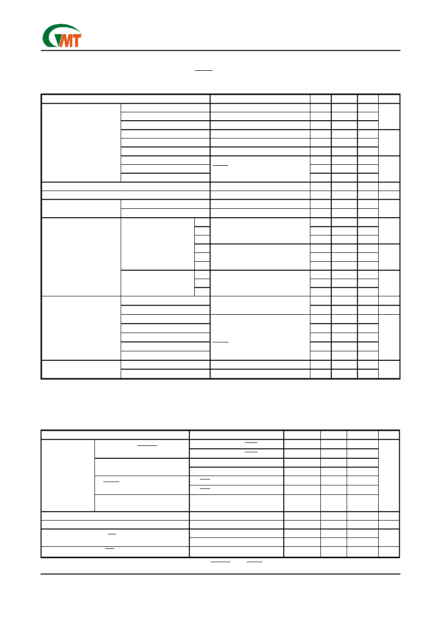
Electrical Characteristics
(T
A
=T
J
=25�C, V
I(5V)
=5V, V
I(3.3V)
=3.3V, V
I(12V)
=12V,
STBY
floating, all outputs unloaded (unless otherwise noted)
DC Characteristics
PARAMETER TEST
CONDITIONS
MIN
TYP MAX UNIT
5V to xVCC
150
180
3.3V to xVCC
V
I(5V)
= 5V, V
I(3.3V)
=3.3V
100
130
3.3V to xVCC
V
I(5V)
= 0V, V
I(3.3V)
=3.3V
110
150
m
5V to xVPP
3
4
3.3V to xVPP
2.9
4
12V to xVPP
1.3
2
3.3V/5V to xVCC
1.2
2
3.3V/5V to xVPP
12
12.5
Switch resistance*
12V to xVPP
STBY
= low, I
O
= 30mA
5
6.5
V
O(xVPP)
Clamp low voltage
I
PP
at 10mA
0.18
0.8
V
V
O(xVCC)
Clamp low voltage
I
CC
at 10mA
0.13
0.8
V
I
PP
high impedance State
T
A
= 25�C
0.3
1
I
IKG
Leakage current
I
CC
high-impedance State
T
A
= 25�C
0.3
1
�A
I
I(3.3V)
6
15
I
I(5V)
110
150
I
I(12V)
V
O(xVCC)
= V
O(xVCC)
= 5V
5 15
�A
I
I(3.3V)
82
150
I
I(5V)
0
Normal operation
and in reset mode
I
I(12V)
V
I(5V)
= 0, V
O(xVCC)
= 3.3V
V
O(xVPP)
= 12V
17 45
�A
I
I(3.3V)
1
I
I(5V)
2
10
I
I
Input current
Shutdown mode
I
I(12V)
V
O(xVCC)
= Hi-Z, V
O(xVPP)
= Hi-Z
1
�A
I
O(xVCC)
0.8 2.2
A
I
O(xVPP)
Output powered into a short to
GND
120 450
mA
Standby mode, 3.3V to xVCC
55
120
Standby mode, 5V to xVCC
70
120
Standby mode, 3.3V to xVPP
44
120
Standby mode, 5V to xVPP
78
120
I
OS
Short-circuit*
Output current Limit
Standby mode, 12V to xVPP
T
J
= 25�C Output powered into a
short to GND
STBY
=0V
60
110
mA
Trip point, TJ
155
Thermal shutdown
Hysteresis
10
�C
* Pulse-testing techniques are used to maintain junction temperature close to ambient temperatures; thermal effects must be taken into ac-
count separately.
Input currents do not include logic input currents (presented in electrical characteristics for logic section); clock is inactive.
Specified by design, not tested in production.
Logic Section
PARAMETER TEST
CONDITION
MIN
TYP
MAX
UNIT
V
I(RESET)
= 5V or V
I
(
RESET
)
= 0V
35
50
I
I
(RESET) or (
RESET
)*
V
I(RESET)
= 0V or V
I
(
RESET
)
=
5V 1
V
I(MODE)
= 5V
35
50
I
I
(MODE)
*
V
I(MODE)
= 0V
1
V
I
(
STBY
)
= 5V
1
I
I
(
STBY
)
*
V
I
(
STBY
)
= 0V
35
50
Logic input cur-
rent
I
I
(CLOCK) or I
I
(DATA) or I
I
(LATCH)
1
�A
Logic input high level
2
V
Logic input low level
2
0.8
V
V
I(5V)
= 5V, I
O
= 1mA
V
I(5V)
0.4
Logic output high level,
OC
V
I(5V)
= 0V, I
O
= 1mA
V
I(3.3V)
0.4
V
Logic output low level,
OC
I
O
= 1mA
0.4
V
*
RESET and MODE have internal 150k
pulldown resistors;
RESET
and
STBY
have internal 150k
pullup resistors.
Ver: 1.0
Jan 23, 2003
TEL: 886-3-5788833
http://www.gmt.com.tw
5
G574
Global Mixed-mode Technology Inc.
Switching Characteristics *, **
PARAMETER TEST
CONDITION
MIN
TYP
MAX
UNIT
V
O (xVCC)
2
t
r
Output rise time
V
O (xVPP)
1
V
O (xVCC)
0.01
t
f
Output fall time
V
O (xVPP)
0.01
ms
t
on
0.2
LATCHto V
O(xVPP)
t
off
1.8
ms
t
on
2.4
LATCHto V
O(xVCC)
(3.3V), V
I(5V)
= 5V
t
off
8.5
ms
t
on
1
LATCHto V
O(xVCC)
(5V)
t
off
8.5
ms
t
on
2.6
t
pd
Propagation delay (see
Figure 1)
LATCHto V
O(xVCC)
(3.3V), V
I(5V)
= 0V
t
off
8.2
ms
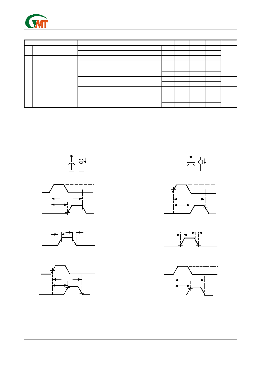
* Refer to Parameter Measurement Information
**Switching Characteristics are with C
L
= 0.1�F
Parameter Measurement Information
Figure 1. Test Circuits and Voltage Waveforms
LOAD CIRCUIT
xVPP
I
O(xVPP)
xVCC
I
O(xCC)
V
DD
GND
50%
90%
t
pd(off)
t
pd(on)
10%
GND
LATCH
V
O(xVPP)
Propagation Delay (xVPP)
90%
10%
t
r
t
f
GND
Rise/Fall Time (xVPP)
V
DD
GND
50%
90%
t
off
t
on
10%
GND
LATCH
V
O(xVPP)
Turn on/off Time (xVPP)
V
DD
GND
50%
90%
t
pd(off)
t
pd(on)
10%
GND
LATCH
V
O(xVCC)
Propagation Delay (xVCC)
90%
10%
t
r
t
f
GND
Rise/Fall Time (xVCC)
V
DD
GND
50%
90%
t
off
t
on
10%
GND
LATCH
V
O(xVCC)
Turn on/off Time (xVCC)
VOLTAGE WAVEFORMS
V
O(xVPP)
V
O(xVCC)