 | –≠–ª–µ–∫—Ç—Ä–æ–Ω–Ω—ã–π –∫–æ–º–ø–æ–Ω–µ–Ω—Ç: G696H263T | –°–∫–∞—á–∞—Ç—å:  PDF PDF  ZIP ZIP |
Ver: 1.1
Jul 26, 2002
TEL: 886-3-5788833
http://www.gmt.com.tw
1
G696/G697
Global Mixed-mode Technology Inc.
Microprocessor Reset IC
Features
Precision Monitoring of +3V, +3.3V, and +5V
Power-Supply Voltages
Fully Specified Over Temperature
Available in Three Output Configurations
Push-Pull RESET Output (G696L)
Push-Pull RESET Output (G696H)
Open-Drain RESET Output (G697L)
Externally Programmable Time Delay Generator
6µA Supply Current
Guaranteed Reset Valid to V
CC
= 0.8V
Power Supply Transient Immunity
5 pin SOT23-5 Packages
Applications
Computers
Controllers
Intelligent Instruments
Critical µP and µC Power Monitoring
Portable / Battery-Powered Equipment
Automotive
General Description
The G696/G697 are microprocessor (µP) supervisory
circuits used to monitor the power supplies in µP and
digital systems. They provide excellent circuit reliability
and low cost and adjustments when used with +5V,
+3.3V, +3.0V- powered circuits.
These circuits perform a single function: they assert a
reset signal whenever the V
CC
supply voltage declines
below a preset threshold, with hysteresis keeping it
asserted for time delay determined by externally pro-
gramable time delay generator. after V
CC
has risen
above the reset threshold. Reset thresholds suitable
for operation with a variety of supply voltages are
available.
The G697L has an open-drain output stage, while the
G696 have push-pull outputs. The G697L's open-drain
RESET output requires a pull-up resistor that can be
connected to a voltage higher than V
CC
. The G696L
have an active-low RESET output, while the G696H
has an active-high RESET output. The reset com-
parator is designed to ignore fast transients on V
CC
,
and the outputs are guaranteed to be in the correct
logic state for V
CC
down to 0.8V.
Low supply current makes the G696/G697 ideal for
use in portable equipment. The G696/G697 are avail-
able in 5-pin SOT23-5 packages.
Ordering Information
PART TEMP.
RANGE PIN-PACKAGE
G696H(L)xxxT1 -40∞C ~ +105∞C SOT23-5
G697LxxxT1
-40∞C ~ +105∞C
SOT23-5
* xxx specifies the threshold voltage.
e.g. 263 denotes the 2.63V threshold voltage.
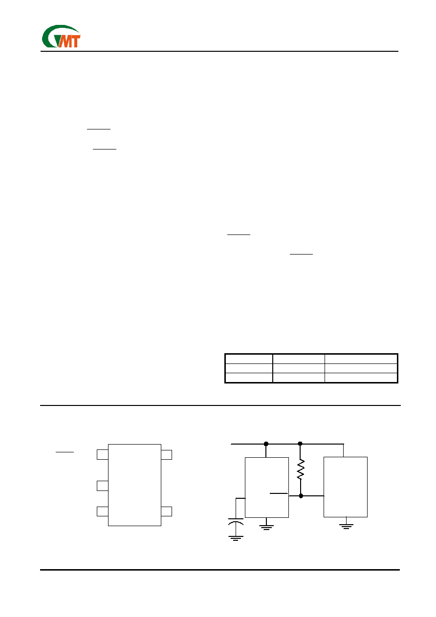
Pin Configuration Typical Operating Circuit
V
CC
SOT23-5
G696/G697
5
1
2
RESET(RESET)
N.C.
4
3
GND
C
D
()is for G696H
*G697 ONLY
RESET
INPUT
GND
µP
V
CC
RESET
(RESET)
GND
G696/G697
V
CC
C
D
V
CC
C
D
R
pull-up*
V
CC
SOT23-5
G696/G697
5
1
2
RESET(RESET)
N.C.
4
3
GND
C
D
()is for G696H
*G697 ONLY
RESET
INPUT
GND
µP
V
CC
RESET
(RESET)
GND
G696/G697
V
CC
C
D
V
CC
C
D
R
pull-up*
Ver: 1.1
Jul 26, 2002
TEL: 886-3-5788833
http://www.gmt.com.tw
2
G696/G697
Global Mixed-mode Technology Inc.
Absolute Maximum Ratings
Terminal Voltage (with respect to GND)
V
CC
..................................................-0.3V to +6.0V
Delay Capacitor Pin Voltage, V
CD
.....-0.3 to (V
CC
+0.3V)
RESET, RESET (push-pull)...........-0.3V to (V
CC
+ 0.3V)
RESET (open drain)...............................-0.3V to +6.0V
Input Current, V
CC
................................................20mA
Output Current, RESET, RESET ........................20mA
Continuous Power Dissipation (T
A
= +70∞C)
5-Pin SOT23-5 (derate 2.17mW/∞C above +70∞C).174mW
Operating Temperature Range ...........-40∞C to +105∞C
Storage Temperature Range...............-65∞C to +150∞C
Lead Temperature (soldering, 10s)...................+300∞C
Stresses beyond those listed under "Absolute Maximum Ratings" may cause p'ermanent damage to the device. These are stress rat-
ings only, and functional operation of the device at these or any other conditions beyond those indicated in the operational sections of
the specifications is not implied. Exposure to absolute maximum rating conditions for extended periods may affect device reliability.
Electrical Characteristics
(V
CC
= full range, T
A
= -40∞C to +105∞C, unless otherwise noted. Typical values are at T
A
= +25∞C, V
CC
= 5V
for 463/438/400 versions, V
CC
= 3.3V for 308/293 versions, and V
CC
= 3V for 263 version.) (Note 1)
PARAMETER SYMBOL
CONDITION
MIN
TYP
MAX
UNITS
T
A
= 0∞C +70∞C
0.8
5.5
V
CC
Range
T
A
= -40∞C +105∞C
1
5.5
V
V
CC
<5.5V, G69_ _463/438/400/330_
6
10
Supply Current (SOT23-5)
I
CC
V
CC
<3.6V, G69_ _308/293/263_
5
8.5
µA
G69_ _463_
4.537 4.63 4.722
G69_ _438_
4.293 4.38
4.467
G69_ _400_
3.92
4
4.08
G69_ _330_
3.234 3.30 3.366
G69_ _308_
3.019 3.08 3.141
G69_ _293_
2.872 2.93 2.988
Reset Threshold
V
TH-
G69_ _263_
2.578 2.63 2.682
V
G69__463_ 139
231
324
G69__438_ 132
219
306
G69__400_ 120
200
280
G69__330_ 99
165
231
G69__308_ 93
154
215
G69__293_ 88
146
205
Reset Threshold Hystersis
V
HYS
G69__263_ 79
131
184
mV
Reset Threshold Tempco
70
ppm/∞C
V
CC
= 5V G69_ _ 463/438/400/330__
3
3.3
3.9
V
V
CC
=3.3V G69_ _308/293
1.9
2.3
2.7
C
D
Delay Pin Threshold Voltage
V
TDC
V
CC
=3.0V G69_ 263_
1.8
2.2
2.6
Delay Capacitor Pin Sink Current
I
CD
V
CC
= 1.5V, V
CD
= 0.5V
3
5
mA
Delay Pull up Resistance
R
D
1
1.5
2.3
M
Ver: 1.1
Jul 26, 2002
TEL: 886-3-5788833
http://www.gmt.com.tw
3
G696/G697
Global Mixed-mode Technology Inc.
Electrical Characteristics
(Continued)
(V
CC
= full range, T
A
= -40∞C to +105∞C, unless otherwise noted. Typical values are at T
A
= +25∞C, V
CC
= 5V
for 463/438/400/330 versions, V
CC
= 3.3V for 308/293 versions, and V
CC
= 3V for 263 version.) (Note 1)
PARAMETER SYMBOL
CONDITION
MIN
TYP
MAX
UNITS
RESET
Output Current Low (push-pull active low,
and open-drain active-low, G696L and G697L)
I
OL
V
CC
= 2.5V, V
RESET
= 0.5V
8 mA
V
CC
= 5V, V
RESET
= 4.5V,
G696L463/438/400/330
4.5
V
CC
= 3.3V, V
RESET
= 2.8V,
G696L308/293
3
RESET
Output Current High (push-pull active
low, G696L)
I
OH
V
CC
= 3V, V
RESET
= 2.5V,
G696L263
2
mA
V
CC
= 5V, V
RESET
= 0.5V,
G696H463/438/400/330
16
V
CC
= 3.3V, V
RESET
= 0.5V,
G696H308/293
12
RESET Output Current Low (push-pull active
high, G696H)
I
OL
V
CC
= 3V, V
RESET
= 0.5V,
G696H263
10
mA
RESET Output Current High (push-pull active
high, G696H)
I
OH
V
CC
= 2.5V, V
RESET
= 2V
2
mA
RESET
Open-Drain Output Leakage Current
(G697L)
V
CC
> V
TH
, RESET deasserted
1 µA
Note 1: Production testing done at T
A
= +25∞C; limits over temperature guaranteed by design.
Selector Guide
PART/SUFFIX
RESET THRESHOLD (V)
OUTPUT TYPE
TOP MARK
G697L463T_ 4.63
Open-Drain
RESET
697Gx
G697L438T_ 4.38
Open-Drain
RESET
697Fx
G697L400T_ 4.00
Open-Drain
RESET
697Ex
G697L330T_ 3.30
Open-Drain
RESET
697Dx
G697L308T_ 3.08
Open-Drain
RESET
697Cx
G697L293T_ 2.93
Open-Drain
RESET
697Bx
G697L263T_ 2.63
Open-Drain
RESET
697Ax
G696H463T_ 4.63
Push-Pull
RESET
696Lx
G696H438T_ 4.38
Push-Pull
RESET
696Kx
G696H400T_ 4.00
Push-Pull
RESET
696Jx
G696H330T_ 3.30
Push-Pull
RESET
696Nx
G696H308T_ 3.08
Push-Pull
RESET
696Ix
G696H293T_ 2.93
Push-Pull
RESET
696Hx
G696H263T_ 2.63
Push-Pull
RESET
696Gx
G696L463T_ 4.63
Push-Pull
RESET
696Fx
G696L438T_ 4.38
Push-Pull
RESET
696Ex
G696L400T_ 4.00
Push-Pull
RESET
696Dx
G696L330T_ 3.30
Push-Pull
RESET
696Mx
G696L308T_ 3.08
Push-Pull
RESET
696Cx
G696L293T_ 2.93
Push-Pull
RESET
696Bx
G696L263T_ 2.63
Push-Pull
RESET
696Ax
Ver: 1.1
Jul 26, 2002
TEL: 886-3-5788833
http://www.gmt.com.tw
4
G696/G697
Global Mixed-mode Technology Inc.
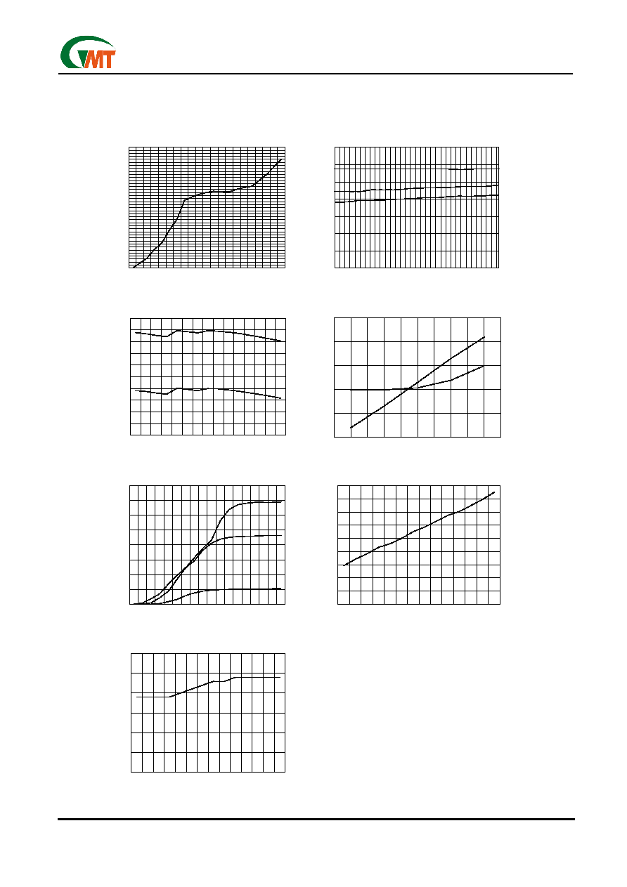
Typical Operating Characteristics
(V
CC
= full range, T
A
= -40∞C to +105∞C, unless otherwise noted. Typical values are at T
A
= +25∞C, V
CC
= 5V
for 463/438/400/330 versions, V
CC
= 3.3V for 308/293 versions, and V
CC
= 3V for 263 version.)
C
D
Delay Pin Sink Current vs. Voltage
0
5
10
15
20
25
30
35
40
3
2.4
1.8
1.2
0.6
0.4
0.2
0.05
V
CD
, Delay Pin Voltage (V)
I
CD
, C
D
DELAY PIN SINK CURRENT (mA)
V
CC
=3V
V
CC
=2.5
V
CC
=1.5V
Output Time Delay vs. Capacitance
0.1
1
10
100
1000
10000
0.0001
0.001
0.01
0.1
1
CD, Delay Pin Capacitance (uF)
Output Time Delay
Delay between V
CC
>V
TH
to output change (ms)
Delay between V
CC
<V
TH
to
output change (us)
Delay Resistance vs. Temperature
1.3
1.35
1.4
1.45
1.5
1.55
1.6
1.65
1.7
1.75
-40
-30
-20
-10
0
10
20
30
40
50
60
70
80
90
T
A
, Ambient Temperature (∞C)
RD, Delay Resistance (M
)
Supply Current vs. V
CC
0
1
2
3
4
5
6
7
8
0 0.6 1 1.2 1.5 1.8 2.1 2.4 2.7 3 3.2 3.3 3.4 3.5 3.7 3.9 4 4.5 5 5.5 6
V
CC
(V)
Supply Current (
u
A)
Reset Output Time Delay vs. Temperature
0
50
100
150
200
250
300
-40 -30
-20
-10
0
10
20
30
40
50
60
70
80
90
T
A
, Ambient Temperature (∞C)
Output Time Delay (ms)
CD=0.1u F
Normalized Reset Threshold vs. Temperature
0.96
0.97
0.98
0.99
1
1.01
1.02
1.03
1.04
1.05
1.06
-40 -30 -20 -10 0
10 20 27 30 40 50 60 70 80 90
T
A
, Ambient Temperature (∞C)
Normalized Ormalized V
TH+
, V
TH-
(V)
V
T
V
TH
Supply Curremt vs. Temperature (No Load)
0
1
2
3
4
5
6
7
-40
-20
0
20
40
60
80
Temperature (∞C)
Supply Current (uA)
V
CC
=5V
V
CC
=3.3V
V
CC
=2.5
Ver: 1.1
Jul 26, 2002
TEL: 886-3-5788833
http://www.gmt.com.tw
5
G696/G697
Global Mixed-mode Technology Inc.
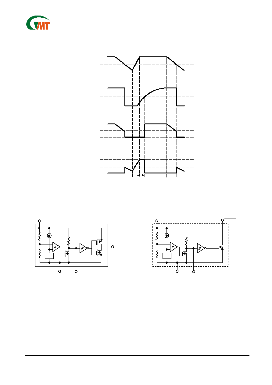
Timing Diagram
Figure 1
Functional Diagram
Figure 2
() is for G696H
2 V
CC
V
TH
RESET
1
3 GND 5 C
D
+
R
D
2 V
CC
V
TH
RESET
(RESET)
1
3 GND 5 C
D
+
R
D
*
() is for G696H
2 V
CC
V
TH
RESET
1
3 GND 5 C
D
+
R
D
2 V
CC
V
TH
RESET
(RESET)
1
3 GND 5 C
D
+
R
D
*
V
CC
V
TH
+
V
TH
-
V
CC
V
CC
V
CC
V
TH
-
V
TH
-
0V
0V
t
D2
V
CC
, Pin 2
C
D
, Pin 5
0.675 V
IN
Reset Output
(Active Low), Pin 1
Reset Output
(Active High), Pin 1
V
CC
V
TH
+
V
TH
-
V
CC
V
CC
V
CC
V
TH
-
V
TH
-
0V
0V
t
D2
V
CC
, Pin 2
C
D
, Pin 5
0.675 V
IN
Reset Output
(Active Low), Pin 1
Reset Output
(Active High), Pin 1
Ver: 1.1
Jul 26, 2002
TEL: 886-3-5788833
http://www.gmt.com.tw
6
G696/G697
Global Mixed-mode Technology Inc.
Pin Description
PIN NAME
FUNCTION
RESET
(G696L/G697L)
RESET
Output remains low while V
CC
is below the reset threshold, and for delay time set by C
D
after V
CC
rises above the reset threshold.
1
RESET (G696H)
RESET Output remains high while V
CC
is below the reset threshold, and for delay time set by C
D
after V
CC
rises above the reset threshold.
2 V
CC
Supply Voltage (+5V, +3.3V, +3.0V)
3 GND
Ground
4 N.C.
No
Connection.
5 C
D
External Programmable time delay is set by the capacitor connect to C
D
pin.
Detailed Description
A microprocessor's (µP's) reset input starts the µP in a
known state. The G697L/G696L/G696H assert reset to
prevent code-execution errors during power-up,
power-down, or brownout conditions. They assert a
reset signal whenever the V
CC
supply voltage declines
below a preset threshold (V
TH-
), keeping it asserted for
time delay set by capacitor connected to C
D
pin, after
V
CC
has risen above the high reset threshold V
TH+
(V
TH-
+V
HYS
). The G697L uses an open-drain output,
and the G696L/G696H have a push-pull output stage.
Connect a pull-up resistor on the G697L's RESET out-
put to any supply between 0 and 5.5V.
The time delay is set by external capacitor C
D
, and
internal pull up resistor R
D
. When the voltage at C
D
pin exceeds the buffer threshold, typically 0.675 V
CC
,
the RESET output high (RESET output low). The
voltage detector and buffer have built-in hysterisis to
prevent erratic reset operation. The formula of time
delay is T (ms)
1685 C
D
(µF). Fig1 and Fig2 show a
timing deagram and a Functional Block.
Figure3.
RESET
Valid to V
CC
= Ground Circuit
Ensuring a Valid Reset Output Down to V
CC
= 0
When V
CC
falls below 0.8V, the G696 RESET output
no longer sinks current--it becomes an open circuit.
Therefore, high-impedance CMOS logic inputs con-
nected to RESET can drift to undetermined voltages.
This presents no problem in most applications since
most µP and other circuitry is inoperative with
VCC
below 0.8V. However, in applications where RESET
must be valid down to 0V, adding a pull-down resistor
to RESET causes any stray leakage currents to flow
to ground, holding RESET low (Figure 4). R1's value
is not critical; 100k
is large enough not to load
RESET and small enough to pull RESET to ground.
A 100k
pull-up resistor to V
CC
is also recommended
for the G697L if RESET is required to remain valid
for V
CC
< 0.8V.
Figure 4. Interfacing to µPs with Bidirectional Reset
I/O
Figure 5. G697L Open-Drain
RESET
Output Allows
Use with Multiple Supplies
V
CC
RESET
GND
G696
R1
100k
V
CC
RESET
GND
G696
R1
100k
RESET
INPUT
GND
µP
V
CC
RESET
GND
G697
V
CC
V
CC
MOTOROLA
68HCXX
R
PULL-UP
RESET
INPUT
GND
µP
V
CC
RESET
GND
G697
V
CC
V
CC
MOTOROLA
68HCXX
R
PULL-UP
RESET
INPUT
GND
5V SYSTEM
V
CC
RESET
GND
G697
V
CC
R
PULL-UP
+3.3V
+5.0
RESET
INPUT
GND
5V SYSTEM
V
CC
V
CC
R
PULL-UP
+3.3V
+5.0V
RESET
INPUT
GND
5V SYSTEM
V
CC
RESET
GND
G697
V
CC
R
PULL-UP
+3.3V
+5.0
RESET
INPUT
GND
5V SYSTEM
V
CC
V
CC
R
PULL-UP
+3.3V
+5.0V
Ver: 1.1
Jul 26, 2002
TEL: 886-3-5788833
http://www.gmt.com.tw
7
G696/G697
Global Mixed-mode Technology Inc.
Interfacing to µPs with Bidirectional Reset Pins
Since the RESET output on the G697L is open drain,
this device interfaces easily with µPs that have bidi-
rectional reset pins, such as the Motorola 68HC11.
Connecting the µP supervisor's RESET output di-
rectly to the microcontroller's (µC's) RESET pin with
a single pull-up resistor allows either device to assert
reset (Figure 5).
G697L Open-Drain
RESET
Output Allows Use with
Multiple Supplies
Generally, the pull-up connected to the G697L will
connect to the supply voltage that is being monitored
at the IC's V
CC
pin. However, some systems may use
the open-drain output to level-shift from the monitored
supply to reset circuitry powered by some other supply
(Figure 6). Note that as the G697L's V
CC
decreases
below 1V, so does the IC's ability to sink current at
RESET . Also, with any pull-up, RESET will be pulled
high as
VCC
decays toward 0. The voltage where this
occurs depends on the pull-up resistor value and the
voltage to which it is connected.
Benefits of Highly Accurate Reset Threshold
Most µP supervisor ICs have reset threshold voltages
between 5% and 10% below the value of nominal
supply voltages. This ensures a reset will not occur
within 5% of the nominal supply, but will occur when
the supply is 10% below nominal.
When using ICs rated at only the nominal supply ±5%,
this leaves a zone of uncertainty where the supply is
between 5% and 10% low, and where the reset may or
may not be asserted.
The G69_ _463/G69_ _308 use highly accurate circuitry
to ensure that reset is asserted close to the 5% limit,
and long before the supply has declined to 10% below
nominal.
Ver: 1.1
Jul 26, 2002
TEL: 886-3-5788833
http://www.gmt.com.tw
8
G696/G697
Global Mixed-mode Technology Inc.
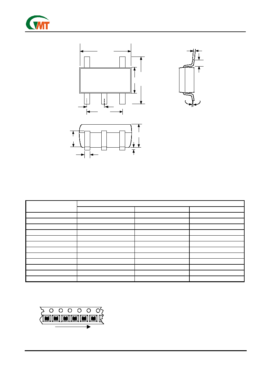
Package Information
Note:
1. Package body sizes exclude mold flash protrusions or gate burrs
2. Tolerance ±0.1000 mm (4mil) unless otherwise specified
3. Coplanarity: 0.1000mm
4. Dimension L is measured in gage plane
DIMENSIONS IN MILLIMETERS
SYMBOLS
MIN NOM MAX
A 1.00 1.10 1.30
A1 0.00 ----- 0.10
A2 0.70 0.80 0.90
b 0.35 0.40
0.50
C 0.10 0.15 0.25
D 2.70 2.90 3.10
E 1.40 1.60 1.80
e -----
1.90(TYP)
-----
e1 ----- 0.95 -----
H 2.60 2.80 3.00
L 0.37 ------ -----
1
1∫ 5∫ 9∫
Taping Specification
GMT Inc. does not assume any responsibility for use of any circuitry described, no circuit patent licenses are implied and GMT Inc. reserves the right at any time without notice to change said circuitry and specifications.
E
e
D
H
1
L
C
b
A2
A1
A
e1
E
e
D
H
1
L
C
b
A2
A1
A
e1
Feed Direction
SOT23-5 Package Orientation
Feed Direction
SOT23-5 Package Orientation