Ver: 1.4
Apr 11, 2005
TEL: 886-3-5788833
http://www.gmt.com.tw
1
G905
Global Mixed-mode Technology Inc.
2.5V 600mA Low Dropout Regulator
Features
Dropout voltage typically 0.8V @ I
O
= 600mA
Output current in 600mA
Output voltage accuracy +2%
Quiescent current, typically 0.3mA
Internal short circuit current limit
Internal over temperature protection
Application
CD-R/W
DVD-ROM
DVD player
LAN Switch
Broadband access
General Description
The G905 positive 2.5V voltage regulator features the
ability to source 600mA of output current with a dropout
voltage of typically 0.8V. A low quiescent current is pro-
vided. The typical quiescent current is 0.3mA.
Familiar regulator features such as over temperature
and over current protection circuits are provided to
prevent it from being damaged by abnormal operating
conditions.
Ordering Information
PIN OPTION
ORDER
NUMBER
ORDER NUMBER
(Pb free)
TEMP.
RANGE
PACKAGE
1 2 3
G905T2
4
U G905T2
4
Uf
-40�C to 85�C
SOT-89
GND
V
IN
V
OUT
Order Number Identification
GXXX XX X X
Packing Type
Pin Option
Package Type
Part Number
PACKAGE TYPE
PIN OPTION
PACKING
T2 : SO-T89
1
2
3
U & D : Tape & Reel Direction
4 : GND
V
IN
V
OUT
Package Type Typical Application
[Note 4] : Type of C
OUT
Top View
1
2
3
SOT-89
V
IN
G905
C1
1�F
IQ
V
OUT
I
O
C
OUT
10�F
Top View
1
2
3
SOT-89
V
IN
G905
C1
1�F
IQ
V
OUT
I
O
C
OUT
10�F

Ver: 1.4
Apr 11, 2005
TEL: 886-3-5788833
http://www.gmt.com.tw
2
G905
Global Mixed-mode Technology Inc.
Absolute Maximum Ratings
(Note 1)
Input Voltage...................................................7V
Power Dissipation Internally Limited................(Note2)
Maximum Junction Temperature.....................150�C
Storage Temperature Range........-65�C
T
J
+150�C
Reflow Temperature (soldering, 10sec)............260�C
Thermal Resistance Junction to Ambient, (
JA
)
SOT-89..................................................173�C/W
Thermal Resistance Junction to Case, (
Jc
)
SOT-89....................................................25�C/W
Note (1):
See Recommended Minimum Footprint
Operating Conditions
(Note 1)
Input Voltage..........................................3.3V ~ 6V
Temperature Range.......................-40�C
T
A
85�C
Electrical Characteristics
V
IN
=5V, I
O
= 600mA, C
IN
=1�F, C
OUT
=10�F. All specifications apply for T
A
= T
J
= 25�C. [Note 3]
PARAMETER CONDITION MIN
TYP
MAX
UNIT
Output Voltage
10mA < I
O
< 600mA
2.45 2.5 2.55 V
Line Regulation
4V < V
IN
< 6V, I
O
= 10mA
---
15
---
mV
Load Regulation
10mA < I
O
< 600mA
---
10
---
mV
Quiescent Current
V
IN
= 5V
---
0.3
---
mA
Ripple Rejection
f
i
= 120Hz, V
ripple
=2V
P-P
, Io = 100mA
---
47
---
dB
I
O
= 600mA
---
800
---
Dropout Voltage
I
O
= 300mA
---
400
---
mV
Output Current
Continuous Test, V
IN
= 3.3V
T
A
= 25�C, T
J
< 125�C, V
OUT
within �2% (Note 3)
Minimum
footprint
--- 600 --- mA
Short Circuit Current
---
0.65
---
A
Current Limit
---
0.8
---
A
Over Temperature
---
145
---
�C
Note 1:
Absolute Maximum Ratings are limits beyond which damage to the device may occur. Operating Conditions are
conditions under which the device functions but the specifications might not be guaranteed. For guaranteed specifications
and test conditions see the Electrical Characteristics.
Note 2:
The maximum power dissipation is a function of the maximum junction temperature, T
Jmax
; total thermal resistance,
JA
,
and ambient temperature T
A
. The maximum allowable power dissipation at any ambient temperature is T
jmax
-T
A
/
JA
. If
this dissipation is exceeded, the die temperature will rise above 150�C and IC will go into thermal shutdown. For the
G905 in SOT-89 (T2) package,
JA
is 173�C/W (See recommend minimum footprint). The safe operation in SOT-89
package, it can see "Typical Performance Characteristics" (Safe Operating Area).
Note3:
Low duty pulse techniques are used during test to maintain junction temperature as close to ambient as possible.
Note4:
The type of output capacitor should be tantalum or aluminum.
Definitions
Dropout Voltage
The input/output Voltage differential at which the regu-
lator output no longer maintains regulation against
further reductions in input voltage. Measured when the
output drops 100mV below its nominal value, dropout
voltage is affected by junction temperature, load cur-
rent and minimum input supply requirements.
Line Regulation
The change in output voltage for a change in input
voltage. The measurement is made under conditions
of low dissipation or by using pulse techniques such
that average chip temperature is not significantly af-
fected.
Load Regulation
The change in output voltage for a change in load
current at constant chip temperature. The measure-
ment is made under conditions of low dissipation or by
using pulse techniques such that average chip tem-
perature is not significantly affected.
Maximum Power Dissipation
The maximum total device dissipation for which the
regulator will operate within specifications.
Quiescent Bias Current
Current which is used to operate the regulator chip
and is not delivered to the load.
Ver: 1.4
Apr 11, 2005
TEL: 886-3-5788833
http://www.gmt.com.tw
4
G905
Global Mixed-mode Technology Inc.
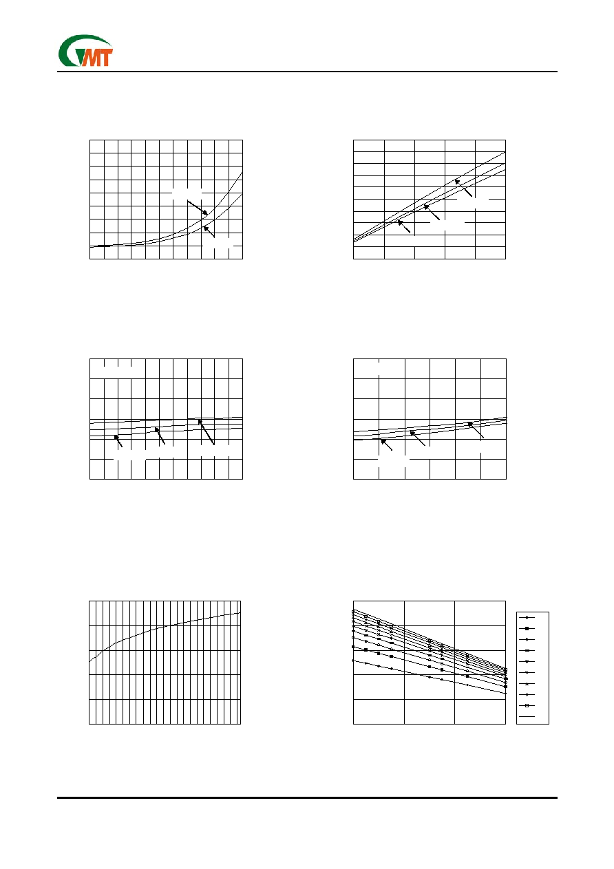
Typical Performance Characteristics
(continued)
0
100
200
300
400
500
600
700
800
900
-25 -15 -5
5
15 25 35 45 55 65 75 85
Temperature (�C)
Q
u
i
e
s
c
ent C
u
r
r
ent
(
�
A
)
V
IN
=4V
V
IN
=5V
0
100
200
300
400
500
600
700
800
900
1000
100
200
300
400
500
600
I
L
(mA)
D
r
opo
ut
V
o
l
t
ag
e
(
m
V
)
T
A
=25�C
T
A
=85�C
2.45
2.48
2.50
2.53
2.55
2.58
2.60
-25 -15 -5
5
15 25 35 45 55 65 75 85
Temperature (�C)
O
u
tput V
o
l
t
age
(
V
)
I
L
=10mA
V
IN
=4V
V
IN
=5V
V
IN
=6V
2.45
2.475
2.5
2.525
2.55
2.575
2.6
3
3.5
4
4.5
5
5.5
6
V
IN
(V)
O
u
tput V
o
l
t
age
(
V
)
IL=10mA
Quiescent Current vs. Temperature
Dropout Voltage vs.I
L
T
A
=-25�C
Output Voltage vs. Temperature
Output Voltage vs. V
IN
T
A
=-25�C
T
A
=25�C
T
A
=85�C
0
0.5
1
1.5
2
2.5
0.5
1.5
2.5
3.5
4.5
PCB Top Copper Area (in
2
)
M
a
x
.
D
i
s
s
i
p
a
t
i
o
n
P
o
w
e
r
(W
)
SOT-89 Max. Power Dissipation
vs. PCB Top Copper Area
T
AMB
= 25�C ; Still Air
SOT-89 Max. Power Dissipation
vs. T
AMB
(still air)
( Different PCB Top Copper Area )
0
0.5
1
1.5
2
2.5
25
45
65
85
T
AMB
(�C)
M
a
x
.
D
i
s
s
i
pati
on P
o
w
e
r
(
W
)
A=0.5
A=1.0
A=1.5
A=2.0
A=2.5
A=3.0
A=3.5
A=4.0
A=4.5
A=5.0
Unit:in
2
Ver: 1.4
Apr 11, 2005
TEL: 886-3-5788833
http://www.gmt.com.tw
6
G905
Global Mixed-mode Technology Inc.
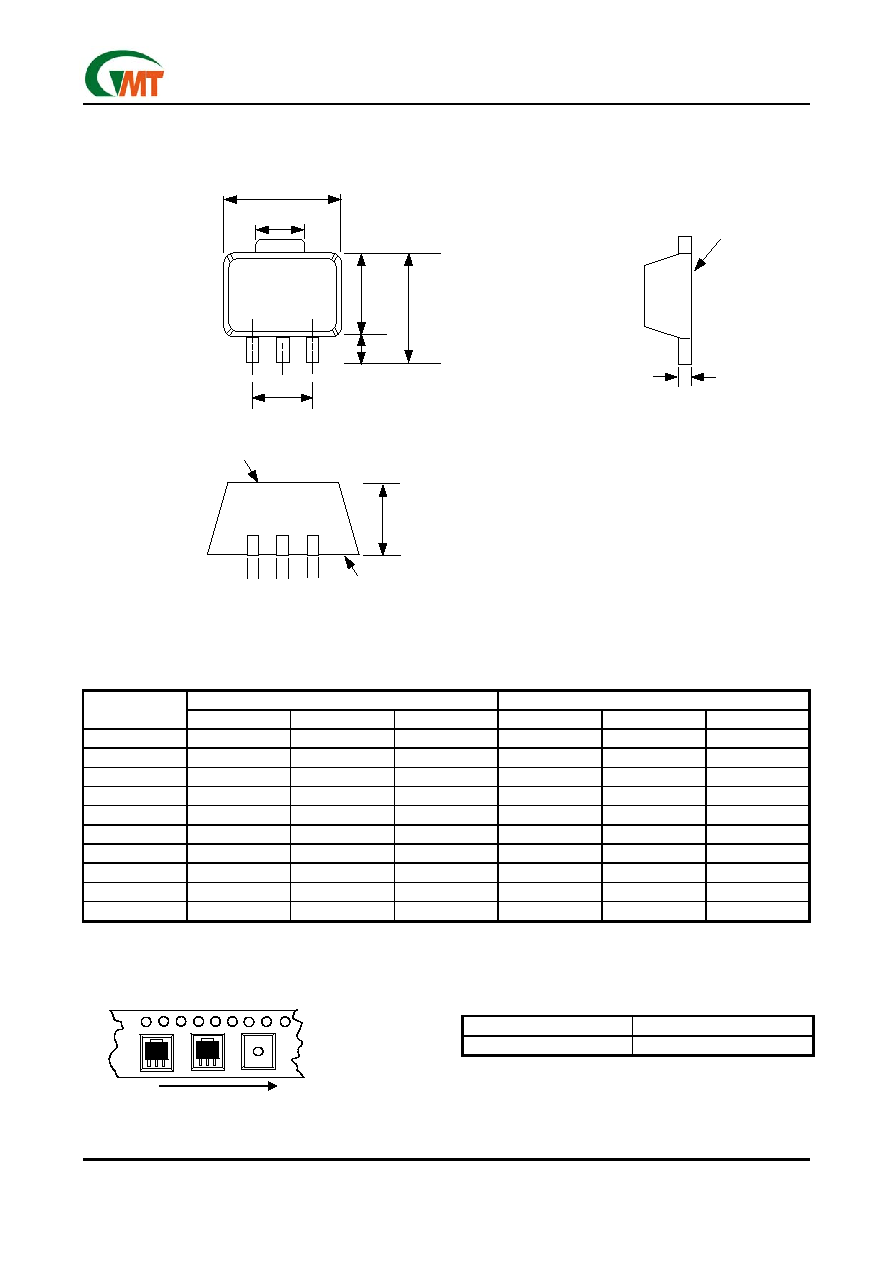
Package Information
SOT-89 (T2) Package
DIMENSIONS IN MILLIMETER
DIMENSIONS IN INCH
SYMBOL
MIN NOM MAX MIN NOM MAX
A 1.40
1.50
1.60
0.055
0.059
0.063
A1 0.80 1.04 ----- 0.031 0.041 -----
b 0.36
0.42
0.48
0.014
0.016
0.019
b1 0.41 0.47 0.53
0.016
0.018
0.020
C 038
0.40
0.43
0.014
0.015
0.017
D 4.40
4.50
4.60
0.173
0.177
0.181
D1 1.40 1.60 1.75
0.055
0.062
0.069
HE ----- ----- 4.25 ----- ----- 0.167
E 2.40
2.50
2.60
0.094
0.098
0.102
e 2.90
3.00
3.10
0.114
0.118
0.122
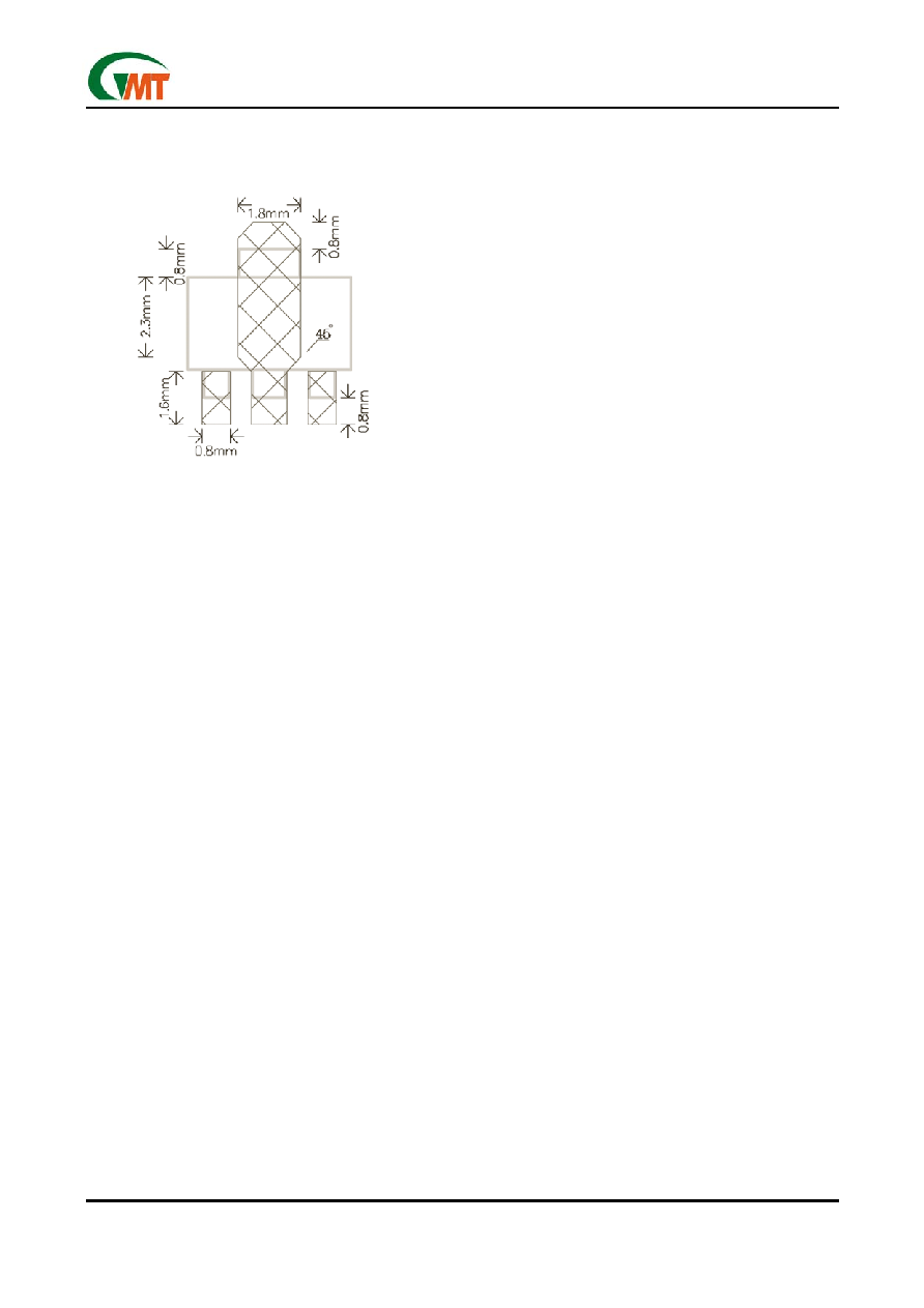
Taping Specification
PACKAGE Q'TY/REEL
SOT-89 1,000
ea
GMT Inc. does not assume any responsibility for use of any circuitry described, no circuit patent licenses are implied and GMT Inc. reserves the right at any time without notice to change said circuitry and specifications.
D
D1
E
A1
HE
e
b
b
b1
A
POLISH
MATTE FINISH
C
POLISH
D
D1
E
A1
HE
e
b
b
b1
A
POLISH
MATTE FINISH
C
POLISH
Feed Direction
SOT-89 Package Orientation
Feed Direction
SOT-89 Package Orientation