 | –≠–ª–µ–∫—Ç—Ä–æ–Ω–Ω—ã–π –∫–æ–º–ø–æ–Ω–µ–Ω—Ç: G9125TJ1U | –°–∫–∞—á–∞—Ç—å:  PDF PDF  ZIP ZIP |

Ver: 0.6 Preliminary
Nov 11, 2005
TEL: 886-3-5788833
http://www.gmt.com.tw
1
G9125
Global Mixed-mode Technology Inc.
2.5V 1A Low Dropout Regulator with Disable
Features
Dropout voltage 0.6V @ I
O
= 1A
Output current in excess of 1A
Output voltage accuracy ±2.5%
Quiescent current, typically 5mA
Internal short circuit current limit
Internal over temperature protection
TO-220 4pin Full-Mold, TO-252-5 package
ON/OFF control
General Description
The G9125 positive 2.5V voltage regulator features
the ability to source 1A of output current. The dropout
voltage is 0.6V at 1A output current. The typical qui-
escent current is 5mA. Furthermore, the quiescent
current is smaller when the regulator is in the dropout
mode.
Familiar regulator features such as over tem-
perature and over current protection circuits are
provided to prevent it from being damaged by
abnormal operating conditions. A V
dis
pin is pro-
vided to disable the output when needed.
Ordering Information
PIN OPTION
ORDER
NUMBER
ORDER NUMBER
(Pb free)
MARKING
TEMP.
RANGE
PACKAGE
1 2 3 4
G9125TF1T
G9125TF1Tf
G9125
-40∞C to +85∞C TO-220F-4
V
IN
V
O
GND V
dis
G9125TH1T
G9125TH1Tf
G9125
-40∞C to +85∞C TO-220F-4
V
IN
V
O
GND V
dis
G9125TJU
G9125TJUf
G9125
-40∞C to +85∞C
TO-252-5
Order Number Identification
GXXXX XX X X
Packing Type
Pin Option
(only TO-220F-4)
Package Type
Part Number
PACKAGE TYPE
PIN OPTION
(only TO-220F-4)
PACKING
TF: TO220F-4 (short lead)
1 2 3 4
T : Tube
TH: TO220F-4 (long lead)
1.: V
IN
V
O
GND V
dis
U: Tape & Reel
TJ:
TO-252-5
Package Type Typical Application
V
IN
G9125
C1
4.7µF
IQ
V
OUT
I
O
C
OUT
47µF
1
2
3
TO-220F-4
4
ON/OFF
TO-252-5
Top View
1
3
2
4
5
VIN V
dis
NC GND
VO
V
IN
G9125
C1
4.7µF
IQ
V
OUT
I
O
C
OUT
47µF
1
2
3
TO-220F-4
4
ON/OFF
TO-252-5
Top View
1
3
2
4
5
VIN V
dis
NC GND
VO
Ver: 0.6 Preliminary
Nov 11, 2005
TEL: 886-3-5788833
http://www.gmt.com.tw
2
G9125
Global Mixed-mode Technology Inc.
Absolute Maximum Ratings
(Note 1)
Input Voltage.....................................................8V
V
dis
Voltage......................................................8V
Power Dissipation Internally Limited (Note 2)
Maximum Junction Temperature.........................150∞C
Storage Temperature Range.........-65∞C
T
J
+150∞C
Reflow Temperature (Soldering, 10 sec)...........260∞C
Continuous Power Dissipation (T
A
= +25∞C)
TO-220 No heatsink.......................................1.5W
TO-220 with infinite heatsink.............................15W
Thermal Resistance Junction to Ambient, (
JA
)
TO-252-5................................................95∞C/W
Thermal Resistance Junction to Case, (
JC
)
TO-252-5......................................................8∞C/W
Operating Conditions
(Note 1)
Input Voltage.............................................3.6V~7V
Temperature Range........................-40∞C
T
A
85∞C
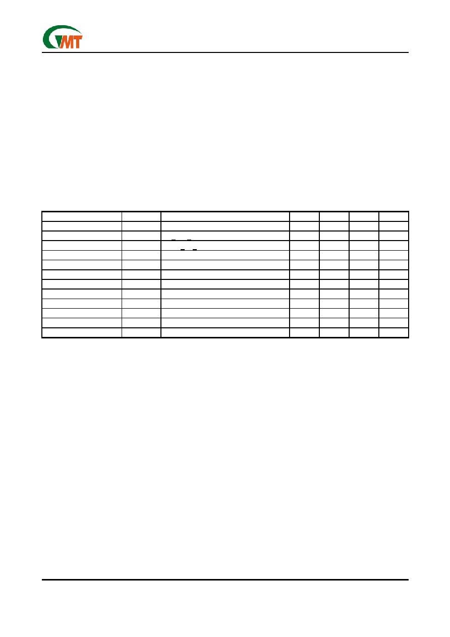
Electrical Characteristics
V
IN
=5V, I
O
= 0.5A, C
IN
= 4.7µF, C
OUT
=47µF, T
A
= T
J
= 25∞C unless otherwise specified [Note 3]
PARAMETER SYMBOL
CONDITION
MIN
TYP
MAX
UNIT
Output Voltage
I
O
=0.5A
2.44 2.5 2.56 V
Line Regulation
4V < V
IN
< 7V, I
O
= 10mA
---
0.5
2
%
Load Regulation
50mA < I
O
< 1A
---
0.5
2
%
Quiescent Current
V
IN
= 5V
---
5
10
mA
Ripple Rejection
fi = 120Hz, 1VP-P, I
O
= 100mA
---
45
---
dB
Dropout Voltage
I
O
= 1A
---
0.4
0.6
V
Short Circuit Current
---
3.8
---
A
Over Temperature
---
150
---
∞C
Disable Voltage High
V
disH
Output
Active
2.0
---
---
V
Disable Voltage Low
V
disL
Output
Disabled
---
---
0.8
V
Disable Bias Current High
I
disH
V
dis
= 2.7V
---
---
20
µA
Disable Bias Current Low
I
disL
V
dis
= 0.4V
---
---
20
µA
Note 1: Absolute Maximum Ratings are limits beyond which damage to the device may occur. Operating Conditions are
conditions under which the device functions but the specifications might not be guaranteed. For guaranteed specifications
and test conditions see the Electrical Characteristics.
Note 2: The maximum power dissipation is a function of the maximum junction temperature, T
Jmax
; total thermal resistance,
JA
, and ambient temperature T
A
. The maximum allowable power dissipation at any ambient temperature is T
jmax
-T
A
/
JA
. If this dissipation is exceeded, the die temperature will rise above 150∞C and IC will go into thermal shutdown. For
the TO-220 package,
JA
is 60∞C/W (No heat sink).
Note3: Low duty pulse techniques are used during test to maintain junction temperature as close to ambient as possible.
Note4: The type of output capacitor should be tantalum or aluminum.
Definitions
Dropout Voltage
The input/output Voltage differential at which the regu-
lator output no longer maintains regulation against fur-
ther reductions in input voltage. Measured when the
output drops 2% below its nominal value, dropout volt-
age is affected by junction temperature, load current
and minimum input supply requirements.
Line Regulation
The change in output voltage for a change in input
voltage. The measurement is made under conditions of
low dissipation or by using pulse techniques such that
average chip temperature is not significantly affected.
Load Regulation
The change in output voltage for a change in load
current at constant chip temperature. The measure-
ment is made under conditions of low dissipation or
by using pulse techniques such that average chip
temperature is not significantly affected.
Maximum Power Dissipation The maximum total de-
vice dissipation for which the regulator will operate
within specifications
.
Quiescent Bias Current
Current which is used to operate the regulator chip
and is not delivered to the load.
Ver: 0.6 Preliminary
Nov 11, 2005
TEL: 886-3-5788833
http://www.gmt.com.tw
3
G9125
Global Mixed-mode Technology Inc.
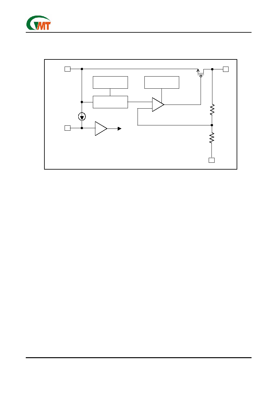
Block Diagram
SHORT-CIRCUIT
PROTECTION
THERMAL
SHUTDOWN
BANDGAP
REFERENCE
3
GND
2 V
O
1
V
IN
R1
R2
1.25V
_
+
OUTPUT
ON/OFF
4
HIGH / LOW
V
dis
TTL COMPATIBLE BUFFER
SHORT-CIRCUIT
PROTECTION
THERMAL
SHUTDOWN
BANDGAP
REFERENCE
3
GND
2 V
O
1
V
IN
R1
R2
1.25V
_
+
_
+
OUTPUT
ON/OFF
4
HIGH / LOW
V
dis
TTL COMPATIBLE BUFFER

Ver: 0.6 Preliminary
Nov 11, 2005
TEL: 886-3-5788833
http://www.gmt.com.tw
4
G9125
Global Mixed-mode Technology Inc.
Typical Performance Characteristics
(V
IN
=5V, C
IN
=10µF, C
OUT
= 10µF, T
A
=25∞C, unless otherwise noted.)
0
10
20
30
40
50
60
10
100
1000
10000
100000
1000000
Frequency (Hz)
Ripple Rejection (dB)
I
L=
1A
I
L=
100mA
Load Transient Response
Line Transient Response
Short Circuit-Current
Output Noise
Disable- ON
Ripple Rejection

Ver: 0.6 Preliminary
Nov 11, 2005
TEL: 886-3-5788833
http://www.gmt.com.tw
5
G9125
Global Mixed-mode Technology Inc.
Typical Performance Characteristics
(continued)
0
100
200
300
400
500
600
-45
-20
5
30
55
80
105
Temperature
Dropout Voltage (m
V)
I
L=
1A
-0.09
-0.08
-0.07
-0.06
-0.05
-0.04
-0.03
-0.02
-0.01
0
-45
-20
5
30
55
80
105
Temperature
Output Voltage Deviation (m
V)
V
IN=
3V
V
IN=
5V
2.49
2.495
2.5
2.505
2.51
2.515
2.52
2.525
2.53
2.535
-45
-20
5
30
55
80
105
Temperature
V
OU
T
(V)
0
0.5
1
1.5
2
2.5
3
3.5
4
-45
-20
5
30
55
80
105
Temperature
Quiescent Current (m
A)
V
IN=
3V
V
IN=
5V
Dropout Voltage vs. Temperature
Load Regulation
Output Voltage vs. Temperature
I
L
=0.5A
V
IN=
5V
V
IN=
3V
Quiescent Current vs. Temperature
0
1
2
3
4
5
0
0.5
1
1.5
2
2.5
3
Disable Voltage Vdis(V)
Output Voltage V
OU
T
(V)
0
1
2
3
4
5
0
1
2
3
4
5
6
7
Input Voltage V
IN
(V)
Output Voltage V
OU
T
(V)
I
L
=0A
I
L
=1A
Output Voltage vs. Input Voltage
Output Voltage vs. Disable Voltage
Ver: 0.6 Preliminary
Nov 11, 2005
TEL: 886-3-5788833
http://www.gmt.com.tw
6
G9125
Global Mixed-mode Technology Inc.
Typical Performance Characteristics
(continued)
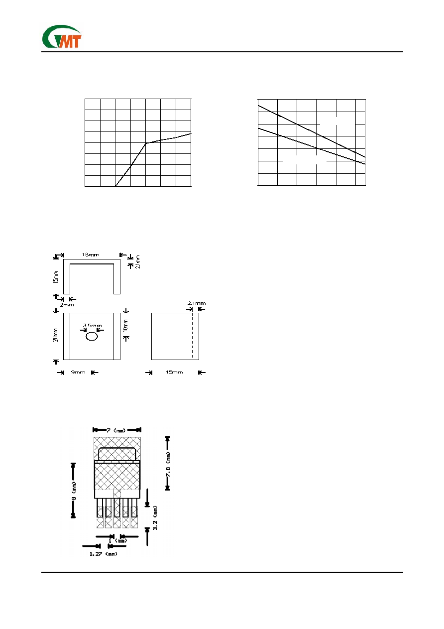
Heatsink Package Dimension
TO-220F-4
Recommended Minimum Footprint
0.0
0.5
1.0
1.5
2.0
2.5
3.0
3.5
4.0
0
1
2
3
4
5
6
7
Input Voltage V
IN
(V)
Quiescent Current IQ(m
A)
Quiescent Current vs. Input Voltage
0
0.5
1
1.5
2
2.5
3
3.5
-25
-5
15
35
55
75
Temperature (T
A
)
Power dissipation Pd (W)
Power Dissipation vs. Temperature (T
A
)
without heatsink
heatsink (5in
2
)
TO-252-5
TO-252-5

Ver: 0.6 Preliminary
Nov 11, 2005
TEL: 886-3-5788833
http://www.gmt.com.tw
7
G9125
Global Mixed-mode Technology Inc.
Package Information
TO-220F-4 Package (short lead)
DIMENSION IN MM
DIMENSION IN INCH
SYMBOL
MIN. NOM. MAX. MIN. NOM. MAX.
A 4.42 4.57 4.72 0.174 0.180 0.186
A1 2.69 2.79 2.89 0.106 0.110 0.114
A2 1.68 1.78 1.88 0.066 0.070 0.074
D 10.00 10.10 10.20 0.394 0.398 0.402
E 6.85 6.95 7.05 0.269 0.273 0.278
E1 8.54 8.64 8.74 0.336 0.340 0.344
L 8.32 8.52 8.72 0.328 0.335 0.343
L1 16.56 16.66 16.76 0.652 0.656 0.660
L2 3.60 3.70 3.80 0.142 0.146 0.150
He 23.72 24.22 24.72 0.934 0.953 0.93
C ----- 0.48 ----- ----- 0.019 -----
e -----
2.54(TYP)
----- ----- 0.1(TYP)
-----
b
----- 0.635(TYP) -----
----- 0.025(TYP) -----
4
∞
7
∞
11
∞
4
∞
7
∞
11
∞
D
E
b
E1
e
A
A1
C
A2
L
L1
L2
He
D
E
b
E1
e
A
A1
C
A2
L
L1
L2
He

Ver: 0.6 Preliminary
Nov 11, 2005
TEL: 886-3-5788833
http://www.gmt.com.tw
8
G9125
Global Mixed-mode Technology Inc.
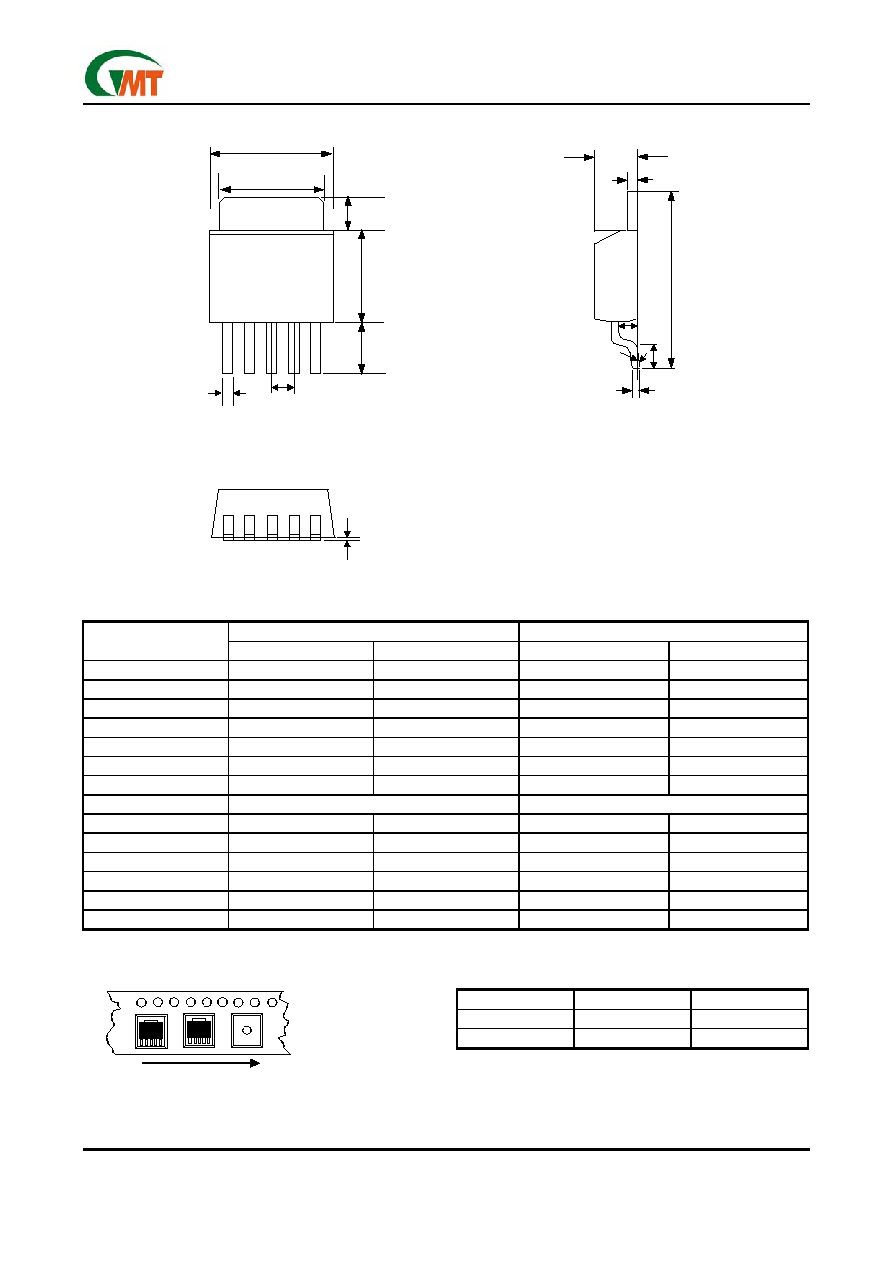
TO-220F-4 Package (long lead)
DIMENSION IN MM
DIMENSION IN INCH
SYMBOL
MIN. NOM. MAX. MIN. NOM. MAX.
A 4.42 4.57 4.72 0.174 0.180 0.186
A1 2.69 2.79 2.89 0.106 0.110 0.114
A2 1.68 1.78 1.88 0.066 0.070 0.074
D 10.00 10.10 10.20 0.394 0.398 0.402
E 6.85 6.95 7.05 0.269 0.273 0.278
E1 8.54 8.64 8.74 0.336 0.340 0.344
L 13.15 13.35 13.55 0.518 0.526 0.533
L1 16.56 16.66 16.76 0.652 0.656 0.660
L2 3.60 3.70 3.80 0.142 0.146 0.150
He 28.44 28.94 29.44 1.119 1.139 1.159
C ----- 0.48 ----- ----- 0.019 -----
e -----
2.54(TYP)
----- ----- 0.1(TYP)
-----
b
----- 0.635(TYP) -----
----- 0.025(TYP) -----
4
∞
7
∞
11
∞
4
∞
7
∞
11
∞
D
E
b
E1
e
A
A1
C
A2
L
L1
L2
He
D
E
b
E1
e
A
A1
C
A2
L
L1
L2
He
Ver: 0.6 Preliminary
Nov 11, 2005
TEL: 886-3-5788833
http://www.gmt.com.tw
9
G9125
Global Mixed-mode Technology Inc.
TO-252-5 (TJ) Package
MILLIMETER INCH
SYMBOL
MIN. MAX. MIN. MAX.
A 2.19
2.38
0.086
0.094
A1 0.89 1.27 0.035
0.050
b 0.64
0.89
0.025
0.035
C 0.46
0.58
0.018
0.023
D 5.36
5.61
0.211
0.221
E 6.35
6.73
0.250
0.265
E1 5.21 5.46 0.205
0.215
e 1.27BSC
0.050BSC
F 0.46
0.58
0.018
0.023
L 1.40
1.78
0.055
0.070
L1 2.20 2.80 0.087
0.110
L2 1.52 2.03 0.060
0.080
H 9.40
10.40
0.370
0.410
0∞ 4∞ 0∞ 4∞
Taping Specification
PACKAGE Q'TY/TUBE Q'TY/REEL
TO-220F-4 50
ea
---
TO-252-5 --- 2,500
ea
GMT Inc. does not assume any responsibility for use of any circuitry described, no circuit patent licenses are implied and GMT Inc. reserves the right at any time without notice to change said circuitry and specifications.
E1
L2
F
A
E
D
L
C
H
A1
b
e
L1
A2
E1
L2
F
A
E
D
L
C
H
A1
b
e
L1
A2
Feed Direction
TO-252-5 Package Orientation
Feed Direction
TO-252-5 Package Orientation