
Ver: 1.6
Dec 22, 2005
TEL: 886-3-5788833
http://www.gmt.com.tw
1
G9131
Global Mixed-mode Technology Inc.
300mA Low-Dropout Linear Regulators
Features
90
µ
A Quiescent Current
Guaranteed 300mA Output Current
Dropout Voltage is 0.4V @ I
O
= 300mA
Over-Temperature Protection and Short-Circuit
Protection
Stable With Low Cost Ceramic Capacitors
Fixed Output Voltage :1.5V, 1.8V, 2.5V, 3.3V
Applications
Cordless Phones
PDAs
Hand-Held Devices
Bar Code Scanners
Electronic Scales
General
Description
The G9131 is a low supply current, low dropout linear
regulator that comes in a space saving SOT-23 pack-
age. The supply current at no-load is 90
µ
A. An over
temperature protection circuit is built-in in the G9131
to prevent thermal overload. These power saving fea-
tures make the G9131 ideal for use in the bat-
tery-powered applications such as notebook com-
puters, cellular phones, and PDA's.
Ordering Information
ORDER
NUMBER
ORDER NUMBER
(Pb free)
MARKING VOLTAGE
TEMP.
RANGE
PACKAGE
G9131-15T73U G9131-15T73Uf
35xx
1.5V
-40
∞
C to +85
∞
C SOT-23
G9131-18T73U G9131-18T73Uf
38xx
1.8V
-40
∞
C to +85
∞
C SOT-23
G9131-25T73U G9131-25T73Uf
32xx
2.5V
-40
∞
C to +85
∞
C SOT-23
G9131-33T73U G9131-33T73Uf
31xx
3.3V
-40
∞
C to +85
∞
C SOT-23
G9131-33T24U G9131-33T24Uf
31xx
3.3V
-40
∞
C to +85
∞
C SOT-89
* For other package types, pin options and package, please contact us at sales@gmt.com.tw
Order Number Identification
GXXXX XX XX X X
Packing Type
Pin Option
Package Type
Voltage
Part Number
PACKAGE TYPE
PIN OPTION
PACKING
T2 : SOT-89
1
2
3
U: Tape & Reel Direction
T7 : SOT-23
1 : V
OUT
GND V
IN
2 : V
OUT
V
IN
GND
3 : GND
V
OUT
V
IN
4 : GND
V
IN
V
OUT
5 : V
IN
GND
V
OUT
6 : V
IN
V
OUT
GND
Package Type
Typical Application
Top View
1
2
3
SOT89
3
Top View
SOT23
1
2
IN
OUT
GND
G9131
C
IN
1
µ
F
OUTPUT
VOLTAGE
C
OUT
1
µ
F
V
IN
Top View
1
2
3
SOT89
3
Top View
SOT23
1
2
IN
OUT
GND
G9131
C
IN
1
µ
F
OUTPUT
VOLTAGE
C
OUT
1
µ
F
V
IN
Ver: 1.6
Dec 22, 2005
TEL: 886-3-5788833
http://www.gmt.com.tw
2
G9131
Global Mixed-mode Technology Inc.
Absolute Maximum Ratings
(Note 1)
Input Voltage.............................................................7V
Power Dissipation Internally Limited (Note2)
Maximum Junction Temperature.........................150
∞
C
Storage Temperature Range.........-65
∞
C
T
J
+150
∞
C
Reflow Temperature (soldering, 10sec) ...........260
∞
C
Thermal Resistance Junction to Ambient, (
JA
)
SOT-23
(1)
.......................................................276
∞
C/W
SOT-89
(1)
......................................... .............173
∞
C/W
Thermal Resistance Junction to Case, (
JC
)
SOT-89......................... ................................. .24
∞
C/W
Note
(1)
: See Recommended Minimum Footprint.
Operating Conditions
(Note 1)
Input Voltage.......................... ...........................3V ~ 6V
Temperature Range...........................-40
∞
C
T
A
85
∞
C
Electrical Characteristics
V
IN
=5V, I
O
= 300mA, C
IN
=1
µ
F, C
OUT
=1
µ
F. All specifications apply for T
A
= T
J
= 25
∞
C. [Note 3]
PARAMETER CONDITION
MIN
TYP
MAX UNIT
V
O
=3.3V
3.234 3.3 3.366
V
O
=2.5V
2.45 2.5 2.55
V
O
=1.8V
1.764 1.8 1.845
Output Voltage
5mA < I
O
< 300mA
V
O
=1.5V
1.455 1.5 1.545
V
Line Regulation
4V < V
IN
< 6V, I
O
= 10mA
--- 15 --- mV
Load Regulation
10mA < I
O
< 300mA
---
10
---
mV
Quiescent Current
V
IN
= 5V
---
90 150
µ
A
Ripple Rejection
f
i
= 120 Hz, 1V
P-P
, Io = 100mA
---
45
---
dB
V
O
=3.3V ---
0.4
---
V
O
=2.5V ---
0.5
---
V
O
=1.8V ---
0.8
---
Dropout Voltage
I
O
= 300mA
V
O
=1.5V ---
0.9
---
V
Short Circuit Current
---
0.65
---
A
Current Limit
---
0.8
---
A
Over Temperature
---
145 ---
∞
C
Over Temperature Hysterics
---
25 ---
∞
C
Note 1: Absolute Maximum Ratings are limits beyond which damage to the device may occur. Operating Conditions are condi-
tions under which the device functions but the specifications might not be guaranteed. For guaranteed specifications and
test conditions see the Electrical Characteristics.
Note 2: The maximum power dissipation is a function of the maximum junction temperature, T
Jmax
; total thermal resistance,
JA
,
and ambient temperature T
A
. The maximum allowable power dissipation at any ambient temperature is T
jmax
-T
A
/
JA
. If this
dissipation is exceeded, the die temperature will rise above 150
∞
C and IC will go into thermal shutdown. For the G9131 in
SOT-23 package,
JA
is 276
∞
C/W and in the SOT-89 package is 173
∞
C/W (See Recommended Minimum Footprint). The
safe operation in SOT-89 & SOT-23 package, it can see "Typical Performance Characteristics" (Safe Operating Area).
Note3: Low duty pulse techniques are used during test to maintain junction temperature as close to ambient as possible.
Note4: The type of output capacitor should be tantalum, aluminum or ceramic.

Ver: 1.6
Dec 22, 2005
TEL: 886-3-5788833
http://www.gmt.com.tw
3
G9131
Global Mixed-mode Technology Inc.
Definitions
Dropout Voltage
The input/output Voltage differential at which the regu-
lator output no longer maintains regulation against
further reductions in input voltage. Measured when the
output drops 100mV below its nominal value, dropout
voltage is affected by junction temperature, load cur-
rent and minimum input supply requirements.
Line Regulation
The change in output voltage for a change in input volt-
age. The measurement is made under conditions of low
dissipation or by using pulse techniques such that av-
erage chip temperature is not significantly affected.
Load Regulation
The change in output voltage for a change in load cur-
rent at constant chip temperature. The measurement is
made under conditions of low dissipation or by using
pulse techniques such that average chip temperature is
not significantly affected.
Maximum Power Dissipation
The maximum total device dissipation for which the
regulator will operate within specifications.
Quiescent Bias Current
Current which is used to operate the regulator chip
and is not delivered to the load.

Ver: 1.6
Dec 22, 2005
TEL: 886-3-5788833
http://www.gmt.com.tw
4
G9131
Global Mixed-mode Technology Inc.
Typical Performance Characteristics
(V
IN
= V
O
+ 1V, C
IN
=1
µ
F, C
OUT
=1
µ
F, T
A
= 25
∞
C, unless otherwise noted.)
Line Transient
Load Transient
3.2
3.22
3.24
3.26
3.28
3.3
3.32
3.34
3.36
3.38
3.4
-45
-25
-5
15
35
55
75
95
115
Temperature (
∞
C)
V
OU
T
(V
)
V
IN
=5V
V
IN
=6V
I
L
=30mA
3.23
3.25
3.27
3.29
3.31
3.33
3.35
3.37
4
4.5
5
5.5
6
6.5
7
V
IN
(V)
V
OU
T
(V
)
V
IN
vs. V
OUT
T=25
∞
C, I
L
=30mA
0
10
20
30
40
50
60
10
100
1000
10000
100000
1000000
Frequency (Hz)
Rip
p
le
Re
je
c
t
i
o
n
(
d
B
)
Ripple Rejection vs. Frequency
100mA
300mA
600mA
88
90
92
94
96
98
100
102
104
106
-25
-5
15
35
55
75
Temperature (
∞
C)
Q
u
i
e
s
c
en
t
C
u
r
r
en
t
(
µ
A
)
V
IN
=5V
V
IN
=6V
Output Voltage vs. Temperature
Quiescent Current vs. Temperature

Ver: 1.6
Dec 22, 2005
TEL: 886-3-5788833
http://www.gmt.com.tw
5
G9131
Global Mixed-mode Technology Inc.
Typical Performance Characteristics
(continue)
Output Noise
Start-Up
Dropout Volatge vs. Temperature
200
250
300
350
400
450
500
550
600
-15
5
25
45
65
85
105
125
Temperature
D
r
opou
t V
o
l
t
age (
m
V
)
I
L
=300mA
v
o
=3.3V
Output Current vs. Output Voltage
SOT-89 Max. Power Dissipation
vs. PCB Top Copper Area
T
AMB
= 25
∞
C ; Still Air
0
0.5
1
1.5
2
2.5
0.5
1
1.5
2
2.5
3
3.5
4
4.5
5
PCB Top Copper Area (in
2
)
Max
.
D
i
s
s
i
pat
i
on
P
o
w
e
r
(
W
)
0
0.5
1
1.5
2
2.5
25
40
55
70
85
T
AMB
(
∞
C)
Max
.
D
i
s
s
i
pat
i
on
P
o
w
e
r
(
W
)
A=0.5
A=1.0
A=1.5
A=2.0
A=2.5
A=3.0
A=3.5
A=4.0
A=4.5
A=5.0
SOT-89 Max. Power Dissipation
vs. T
AMB
(still air)
( Different PCB Top Copper Area )
Unit:in
2
Ver: 1.6
Dec 22, 2005
TEL: 886-3-5788833
http://www.gmt.com.tw
6
G9131
Global Mixed-mode Technology Inc.
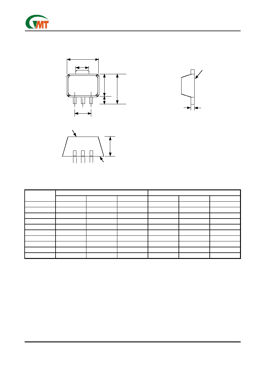
Recommended Minimum Footprint
SOT-23
SOT-89

Ver: 1.6
Dec 22, 2005
TEL: 886-3-5788833
http://www.gmt.com.tw
7
G9131
Global Mixed-mode Technology Inc.
Pin Description
NAME
FUNCTION
IN
Regulator Input. Supply voltage can range from V
IN(min)
to +5.5V. Bypass with 1
µ
F to GND.
GND
This is ground pin.
OUT
Regulator Output. Sources up to 300mA. Bypass with a 1
µ
F,
0.2
typical ESR capacitor to GND.
Detailed Description
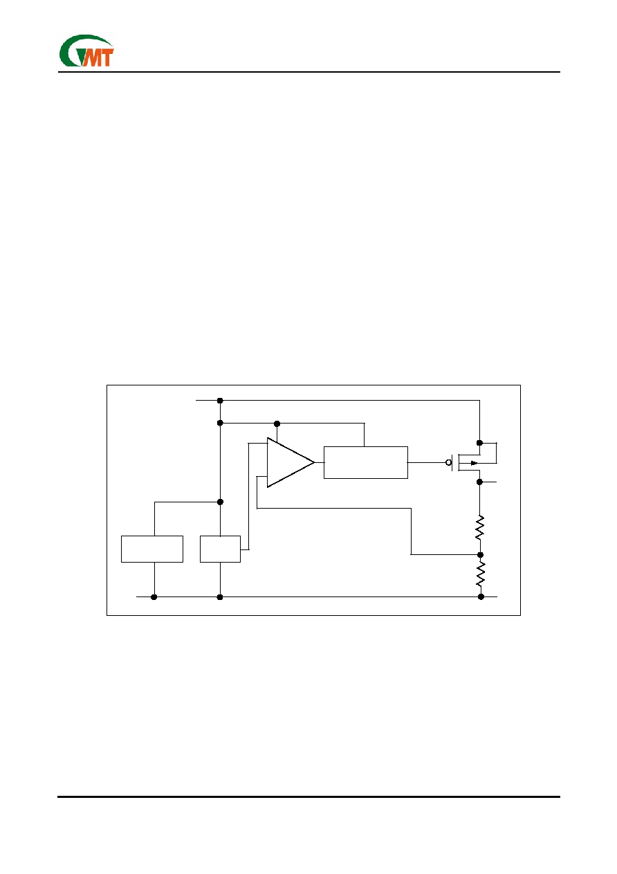
The block diagram of the G9131 is shown in Figure 1.
It consists of an error amplifier, 1.25V bandgap refer-
ence, PMOS output transistor, internal feedback volt-
age divider, over current protection circuit, and over
temperature protection circuit.
Over Current Protection
The G9131 use a current sense-resistor to monitor the
output current. A portion of the PMOS output transistor's
current is mirrored to a resistor such that the voltage
across this resistor is proportional to the output current.
Once the output current exceeds limit threshold, G9131
would be protected with a limited output current. Further
more, when the output is short to ground, the output
current would be folded-back to a less limit.
Over Temperature Protection
To prevent abnormal temperature from occurring, the
G9131 has a built-in temperature monitoring circuit.
When it detects the temperature is above 150
∞
C, the
output transistor is turned off. When the IC is cooled
down to below 135
∞
C, the output is turned on again. In
this way, the G9131 will be protected against abnor-
mal junction temperature during operation.
Operating Region and Power Dissipation
Since the G9131 is a linear regulator, its power dissi-
pation is always given by P = I
OUT
(V
IN
- V
OUT
). The
maximum power dissipation is given by: P
D(MAX)
= (T
J
-
T
A
)/
JA
, Where (T
J
- T
A
) is the temperature difference
the G9131 die and the ambient air. For surface mount
device, heat sinking is accomplished by using the heat
spreading capabilities of the PC board and its copper
traces.
JA
is the thermal resistance of the chosen
package to the ambient air. In the case of a SOT-23
package, the thermal resistance is typically 275.5
∞
C/W.
In SOT 89 R
JA
is 172.5
∞
C/W.
Ver: 1.6
Dec 22, 2005
TEL: 886-3-5788833
http://www.gmt.com.tw
8
G9131
Global Mixed-mode Technology Inc.
Applications Information
Capacitor Selection and Regulator Stability
Normally, use a 1
µ
F capacitor on the input and a 1
µ
F
capacitor on the output of the G9131. Larger input ca-
pacitor values and lower ESR provide better sup-
ply-noise rejection and transient response. For stable
operation over the full temperature range, with load
currents up to 120mA, a minimum of 1
µ
F is recom-
mended.
Power-Supply Rejection and Operation from
Sources Other than Batteries
The G9131 is designed to deliver low dropout voltages
and low quiescent currents in battery powered sys-
tems. Power-supply rejection is 47dB at low frequen-
cies the output capacitor is the major contributor to the
rejection of power-supply noise.
When operating from sources other than batteries,
improve supply-noise rejection and transient response
by increasing the values of the input and output ca-
pacitors, and using passive filtering techniques.
Load Transient Considerations
The G9131 load-transient response graphs show two
components of the output response: a DC shift of the
output voltage due to the different load currents, and
the transient response. Typical overshoot for step
changes in the load current from 0mA to 300mA is
10mV. Increasing the output capacitor's value and
decreasing its ESR attenuates transient spikes.
Input-Output (Dropout) Voltage
A regulator's minimum input-output voltage differential
(or dropout voltage) determines the lowest usable
supply voltage. In battery-powered systems, this will
determine the useful end-of-life battery voltage. Be-
cause the G9131 use a P-channel MOSFET pass
transistor, their dropout voltage is a function of R
DS(ON)
multiplied by the load current.
Figure 1. Functional Diagram
IN
OUT
1.25V
Vref
ERROR
AMP
OVER CURRENT
PROTECT & DYNAMIC
FEEDBACK
GND
R1
R2
OVER TEMP.
PROTECT
P
IN
OUT
1.25V
Vref
ERROR
AMP
OVER CURRENT
PROTECT & DYNAMIC
FEEDBACK
GND
R1
R2
OVER TEMP.
PROTECT
P
Ver: 1.6
Dec 22, 2005
TEL: 886-3-5788833
http://www.gmt.com.tw
9
G9131
Global Mixed-mode Technology Inc.
Package Information
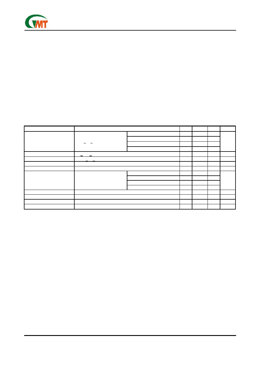
SOT-89 (T2) Package
DIMENSION IN MILLIMETER
DIMENSION IN INCH
SYMBOL
MIN NOM MAX MIN NOM MAX
A 1.40
1.50
1.60
0.055
0.059
0.063
A1 0.80 1.04 ----- 0.031 0.041 -----
b 0.36
0.42
0.48
0.014
0.016
0.018
b1 0.41 0.47 0.53
0.016
0.018
0.020
C 038
0.40
0.43
0.014
0.015
0.017
D 4.40
4.50
4.60
0.173
0.177
0.181
D1 1.40 1.60 1.75
0.055
0.062
0.069
HE ----- ----- 4.25 ----- ----- 0.167
E 2.40
2.50
2.60
0.094
0.098
0.102
e 2.90
3.00
3.10
0.114
0.118
0.122
D
D1
E
A1
HE
e
b
b
b1
A
POLISH
MATTE FINISH
C
POLISH
D
D1
E
A1
HE
e
b
b
b1
A
POLISH
MATTE FINISH
C
POLISH

Ver: 1.6
Dec 22, 2005
TEL: 886-3-5788833
http://www.gmt.com.tw
10
G9131
Global Mixed-mode Technology Inc.
SOT-23 (T7) Package
Note:
1.Package body sizes exclude mold flash protrusions or gate burrs
2.Tolerance
±
0.1000 mm (4mil) unless otherwise specified
3.Coplanarity: 0.1000mm
4.Dimension L is measured in gage plane
DIMENSION IN MILLIMETER
SYMBOL
MIN NOM MAX
A 1.00 1.10
1.30
A1 0.00 ----- 0.10
A2 0.70 0.80 0.90
b 0.35
0.40
0.50
C 0.10 0.15
0.25
D 2.70 2.90
3.10
E 1.40 1.60
1.80
e -----
1.90(TYP)
-----
H 2.60 2.80
3.00
L 0.37
------ -----
1
1
∞
5
∞
9
∞
Taping Specification
PACKAGE Q'TY/BY
REEL
SOT-23 3,000
ea
SOT-89 1,000
ea
GMT Inc. does not assume any responsibility for use of any circuitry described, no circuit patent licenses are implied and GMT Inc. reserves the right at any time without notice to change said circuitry and specifications.
H
D
e
E
L
C
1
b
A2
A
A1
H
D
e
E
L
C
1
b
A2
A
A1
Feed Direction
SOT-89 Package Orientation
Feed Direction
SOT-23 Package Orientation
Feed Direction
SOT-89 Package Orientation
Feed Direction
SOT-23 Package Orientation
Feed Direction
SOT-23 Package Orientation