 | –≠–Ľ–Ķ–ļ—ā—Ä–ĺ–Ĺ–Ĺ—č–Ļ –ļ–ĺ–ľ–Ņ–ĺ–Ĺ–Ķ–Ĺ—ā: G914F | –°–ļ–į—á–į—ā—Ć:  PDF PDF  ZIP ZIP |
Ver: 1.2
Jun 30, 2002
TEL: 886-3-5788833
http://www.gmt.com.tw
1
G914X
Global Mixed-mode Technology Inc.
300mA Low-Noise LDO Regulators
Features
Ultra Low Output Noise
30ĶV (rms)
Ultra Low 55ĶA No-Load Supply Current
Ultra Low Dropout 70mV @ 50mA Load
Guarantee 300mA Output Current
Over-Temperature and Short-Circuit Protection
Fixed: 2.70V (G914A), 2.80V (G914B)
3.00V (G914C), 3.30V (G914D)
2.50V (G914E), 2.85V (G914F)
1.50V(G914G), 1.80V(G914H)
Max. Supply Current in Shutdown Mode < 1ĶA
Stable with low cost ceramic capacitors
Applications
Notebook Computers
Cellular Phones
PDA
Hand-Held Devices
Battery-Powered Application
General Description
The G914X is a low supply current, low dropout linear
regulator that comes in a space saving SOT23-5
package. The supply current at no-load is 55ĶA. In the
shutdown mode, the maximum supply current is less
than 1ĶA. Operating voltage range of the G914X is
from 2.5V to 5.5V. The over-current protection limit is
set at 500mA typical and 400mA minimum. An
over-temperature protection circuit is built-in in the
G914X to prevent thermal overload. These power
saving features make the G914X ideal for use in the
battery-powered applications such as notebook com-
puters, cellular phones, and PDA's.
Ordering Information
ORDER
NUMBER
MARKING VOLTAGE
TEMP.
RANGE
PACKAGE
G914A 4Axx 2.70V
-40įC~
+85įC
SOT
23-5
G914B 4Bxx 2.80V
-40įC~
+85įC
SOT
23-5
G914C 4Cxx 3.00V
-40įC~
+85įC
SOT
23-5
G914D 4Dxx 3.30V
-40įC~
+85įC
SOT
23-5
G914E 4Exx 2.50V
-40įC~
+85įC
SOT
23-5
G914F 4Fxx 2.85V
-40įC~
+85įC
SOT
23-5
G914G 4Gxx 1.50V
-40įC~
+85įC
SOT
23-5
G914H 4Hxx 1.80V
-40įC~
+85įC
SOT
23-5
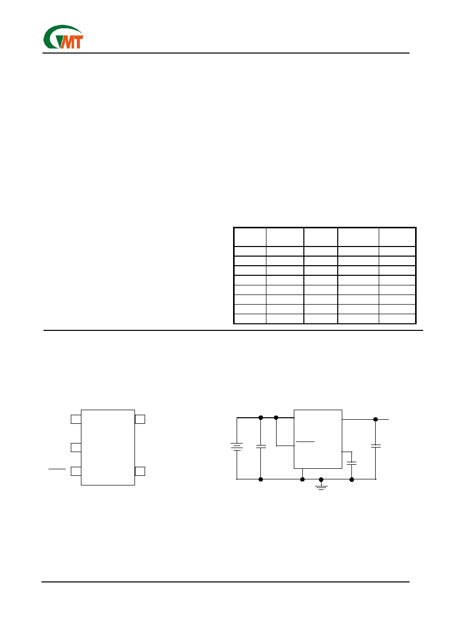
Pin Configuration
Typical Operating Circuit
OUT
BYP
SOT23-5
G914X
5
4
1
IN
2
3
GND
SHDN
IN
OUT
GND
SHDN
G914X
C
IN
1ĶF
_
BATTERY
OUTPUT
VOLTAGE
C
OUT
1
Ķ
F
Fixed mode
BYP
C
BYP
10nF
OUT
BYP
SOT23-5
G914X
5
4
1
IN
2
3
GND
SHDN
IN
OUT
GND
SHDN
G914X
C
IN
1ĶF
_
BATTERY
OUTPUT
VOLTAGE
C
OUT
1
Ķ
F
Fixed mode
BYP
C
BYP
10nF
Ver: 1.2
Jun 30, 2002
TEL: 886-3-5788833
http://www.gmt.com.tw
2
G914X
Global Mixed-mode Technology Inc.
Absolute Maximum Ratings
V
IN
to GND.............................................-0.3V to +7V
Output Short-Circuit Duration.............................Infinite
All Other Pins to GND....................-0.3V to (V
IN
+ 0.3V)
Continuous Power Dissipation (T
A
= +25įC)
SOT 23-5 ....................................................520 mW
Operating Temperature Range...........-40įC to +85įC
Junction Temperature.................................+150įC
JA
(1)
..................................................240įC/Watt
Storage Temperature Range............-65įC to +160įC
Lead Temperature (soldering, 10sec).............+260įC
Note
(1)
: See Recommended Minimum Footprint (Figure 2)
Stresses beyond those listed under "Absolute Maximum Ratings" may cause permanent damage to the device. These are stress ratings
only, and functional operation of the device at these or any other conditions beyond those indicated in the operational sections of the
specifications is not implied. Exposure to absolute maximum rating conditions for extended periods may affect device reliability.
Electrical Characteristics
(V
IN
=V
OUT(STD)
+1V, V
SHDN
=V
IN
, T
A
=T
J
=25įC, unless otherwise noted.) (Note 1)
PARAMETER SYMBOL
CONDITIONS
MIN
TYP
MAX
UNITS
Input Voltage (Note 2)
V
IN
Note2 - 5.5 V
Variation from specified V
OUT
, I
OUT
=1mA,V
OUT
2.5V version -2 - 2
For G914H, I
OUT
=1mA -3
-
3
Output Voltage Accuracy
V
OUT
For G914G, I
OUT
=1mA -4
-
4
%
Maximum Output Current
300
-
mA
Current Limit (Note 3)
I
LIM
500 - mA
I
LOAD
= 0mA
55
120
I
LOAD
= 50mA
145
Ground Pin Current
I
Q
V
IN
=3.6V
I
LOAD
= 300mA
265
ĶA
I
OUT
= 1mA
2
I
OUT
= 50mA, V
OUT
2.7V Version
70
V
O (NOM)
3.0V
230
2.5V
V
O
(NOM)
2.85V
250
V
O (NOM)
= 1.8V
380
I
OUT
= 150mA
V
O (NOM)
= 1.5V
510
V
O (NOM)
3.0V
450
600
2.5V
V
O
(NOM)
2.85V
500
660
V
O (NOM)
= 1.8V
760 960
Dropout Voltage (Note 4)
V
DROP
I
OUT
=300mA
V
O (NOM)
= 1.5V
910 1220
mV
Line Regulation
V
LNR
V
IN
=V
OUT
+100mV to 5.5V, I
OUT
= 1mA
0.1 0.28
%/V
I
OUT
= 1mA to 150mA
0.35
Load Regulation (Note 5)
V
LDR
I
OUT
= 1mA to 300mA
2
%
Power Supply Rejection Ratio
PSRR I
OUT
= 30mA C
BYP
= 10nF, f = 120HZ
57
dB
Output Voltage Temperature Coefficient V
O
/T I
OUT
= 50mA, T
J
= 25įC to 125įC
30
ppm/įC
C
OUT
= 1ĶF, I
OUT
= 150mA, C
BYP
=1nF 52
C
OUT
= 1ĶF, I
OUT
= 150mA, C
BYP
=10nF 35
C
OUT
= 1ĶF, I
OUT
= 150mA, C
BYP
= 100nF
30
Output Voltage Noise
(10Hz to 100kHz)
(G914H)
e
n
V
IN
=V
OUT
+1V
C
OUT
= 1ĶF, I
OUT
= 1mA, C
BYP
= 10nF
26
ĶV
RMS
SHUTDOWN
V
IH
Regulator
enabled
V
IN
- 0.7
SHDN
Input Threshold
V
IL
Regulator
shutdown
0.4
V
SHDN
Input Bias Current
I
SHDN
V
SHDN
= V
IN
T
A
= +25įC
0.003
0.1
Shutdown Supply Current
I
Q SHDN
V
OUT
= 0V
T
A
= +25įC
1
ĶA
THERMAL PROTECTION
Thermal Shutdown Temperature
T
SHDN
150
įC
Thermal Shutdown Hysteresis
T
SHDN
15 įC
Note 1: Limits is 100% production tested at T
A
= +25įC. Low duty pulse techniques are used during test to
maintain junction temperature as close to ambient as possible.
Note 2: V
IN (min)
=V
OUT (STD)
+V
DROPOUT
Note 3: Not tested. For design purposes, the current limit should be considered 400mA minimum to 600mA maximum.
Note 4: The dropout voltage is defined as (V
IN
- V
OUT
) when V
OUT
is 100mV below the value of V
OUT
for V
IN
= V
OUT
+1V. The
performance of every G914X version, see "Typical Performance Characteristics".
Note 5: Regulation is measured at constant junction temperature using low duty cycle pulse testing. Parts are tested for
load regulation in the load range from 1mA to 300mA. Changes in output due to heating effects are covered by the
thermal regulation specification.
Ver: 1.2
Jun 30, 2002
TEL: 886-3-5788833
http://www.gmt.com.tw
3
G914X
Global Mixed-mode Technology Inc.
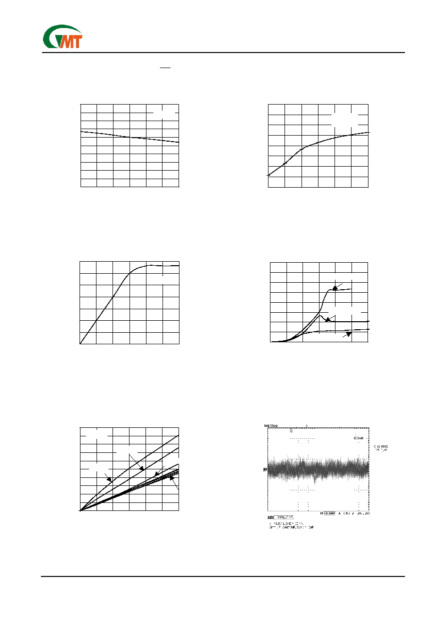
Typical Performance Characteristics
(V
IN
= V
O
+1V, C
IN
=1ĶF, C
OUT
=1ĶF, V
SHDN
= V
IN
, G914D, T
A
=25įC, unless otherwise noted.)
0
50
100
150
200
250
300
350
400
0
1
2
3
4
5
6
Input Voltage (V)
Supply Current (ĶA)
I
LOAD
=300mA
I
LOAD
=50mA
I
LOAD
=0mA
0
50
100
150
200
250
300
350
400
0
50
100
150
200
250
300
Load Current (mA)
Ground Current (ĶA)
V
IN
=3.6V
No Load
3.240
3.250
3.260
3.270
3.280
3.290
3.300
3.310
3.320
3.330
3.340
0
50
100
150
200
250
300
Load Current (mA)
Output Voltage (V)
G914D
0.0
0.5
1.0
1.5
2.0
2.5
3.0
3.5
0
1
2
3
4
5
6
Input Voltage (V)
Output Voltage (V)
No Load
0
100
200
300
400
500
600
700
800
900
1000
0
50
100
150
200
250
300
Loading (mA)
Dropout Voltage (mV)
G914E
G914H
G914G
T
A
=25įC
Top to down
G914A
G914B
G914F
G914C
G914D
Dropout Voltage vs. Load Current
Output Voltage vs. Load Current
Output Voltage vs. Input Voltage
Ground Current vs. Load Current
Supply Current vs. Input Voltage
Ouptut Noise 10HZ to 100KHZ
Ver: 1.2
Jun 30, 2002
TEL: 886-3-5788833
http://www.gmt.com.tw
4
G914X
Global Mixed-mode Technology Inc.
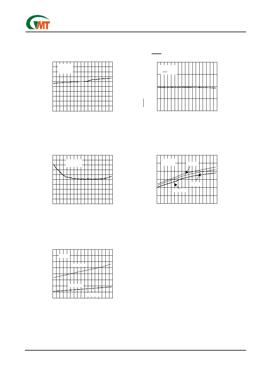
Typical Performance Characteristics
(continued)
-1.00
-0.60
-0.20
0.20
0.60
1.00
-40 -30 -20 -10 0 10 20 30 40 50 60 70 80 90 10
0
11
0
12
0
13
0
Junction Temperature T
J
(įC)
Shutdown Supply Current(ĶA)
G914D
V
IN
= 4.3V
3.24
3.26
3.28
3.30
3.32
3.34
3.36
-40 -30 -20 -10 0 10 20 30 40 50 60 70 80 90 10
0
11
0
12
0
13
0
Junction Temperature T
J
(įC)
Output Voltage (V)
V
IN
=4.3V
V
IN
=3.4V
0
50
100
150
200
250
300
350
400
-40 -30 -20 -10 0 10 20 30 40 50 60 70 80 90 10
0
11
0
12
0
13
0
Junction Temperature T
J
(įC)
Dropout Voltage (mV)
G914D
I
LOAD
=150mA
I
LOAD
=50mA
G914D
I
LOAD
=1mA
I
LOAD
=0mA
0
20
40
60
80
100
-40 -30 -20 -10 0 10 20 30 40 50 60 70 80 90 10
0
11
0
12
0
13
0
Junction Temperature T
J
(įC)
Ground Current (ĶA)
G914D
V
IN
= 4.3V
I
OUT
=0A
-0.20
-0.10
0.00
0.10
0.20
-40 -30 -20 -10 0 10 20 30 40 50 60 70 80 90 10
0
11
0
12
0
13
0
Junction Temperature T
J
(įC)
SHDN Input Bias Current (ĶA)
G914D
V
IN
=4.3V
V
SHDN
=V
IN
V
IN
=5.5V
Ground Current vs. Temperature
SHDN Input Bias Current vs. Temperature
Shutdown Supply Current vs. Temperature
Output Voltage vs. Temperature
Dropout Voltage vs. Temperature

Ver: 1.2
Jun 30, 2002
TEL: 886-3-5788833
http://www.gmt.com.tw
5
G914X
Global Mixed-mode Technology Inc.
Typical Performance Characteristics
(continued)
0
10
20
30
40
50
60
70
0.001
0.01
0.1
Bypass Capacitance (ĶF)
Output Noise (ĶVrms)
0
10
20
30
40
50
60
70
1
10
100
1000
Load Current (mA)
Output Noise (ĶVrms)
G914H
V
IN
=2.8V
T
A
=25įC
G914H
V
IN
=2.8V
T
A
=25įC
C
OUT
=1ĶF
C
OUT
=1ĶF
0
10
20
30
40
50
60
70
80
0.1
1
10
100
Frequency(KHZ)
Power Supply Rejection
Ratio(db)
G914F
V
IN
=5V +2V(p-p)
R
L
=100
C
BYP
=10nF
Line Transient
Load Transient
Power Supply Rejection Ripple
Load Transient
Output Noise vs. Bypass Capacitance
Output Noise vs. Load Current