Ver: 1.7
Jan 25, 2006
TEL: 886-3-5788833
http://www.gmt.com.tw
1
G916
Global Mixed-mode Technology Inc.
300mA High PSRR, Low Noise, LDO Regulators
Features
Low, 90
µ
A No-Load Supply Current
Guaranteed 300mA Output Current
Dropout Voltage is 200mV @ 150mA Load
PSRR=65dB @ 120Hz; 55dB @ 1kHz
Over-Temperature Protection and Short-Circuit
Protection
Fixed Mode: 1.20V~5.00V (G916-XXX)
Adjustable Mode: from 1.25V to 5.50V (G916)
Max. Supply Current in Shutdown Mode < 1
µ
A
Low Output Noise at 28
µ
V
RMS
with bypass Ca-
pacitor
Stable with low cost ceramic capacitors
Applications
Notebook Computers
Cellular Phones
PDAs
Digital still Camera and Video Recorders
Hand-Held Devices
Audio Codec
General
Description
The G916 series is a low supply current, high PSRR,
low noise, and low dropout linear regulator that comes
in a space saving TSOT-23-5, SOT-23-5 package.
The supply current at no-load is 90µA. In the shutdown
mode, the maximum supply current is less than 1µA.
Operating voltage range is from 2.5V to 6.0V. The
over-current protection limit is set at 550mA typical. An
over- temperature protection circuit is built-in in the
Device to prevent thermal overload. These power
saving features make the G916 series ideal for use in
the battery-powered applications such as notebook
computers, cellular phones, and PDA's.
The G916 has two modes of operation. When the SET
pin is connected to ground, its output is a pre-set value:
3.3V. There is no external component needed. When an
output other than the preset value is needed, two ex-
ternal resistors should be used as a voltage divider. The
output voltage is then adjusted by the resistor ratio.
G916-XXX is with fixed-mode output. The output voltage
range is from 1.2V to 5.0V.
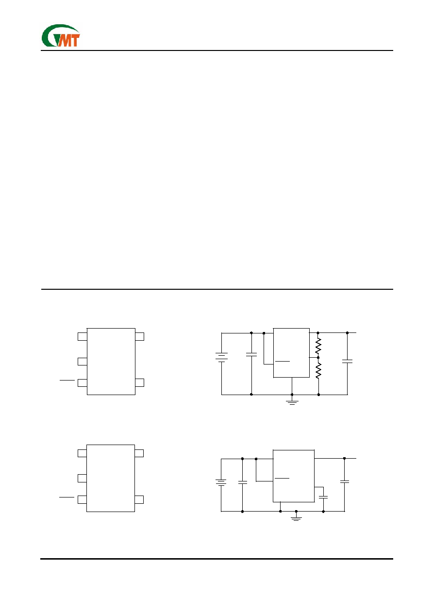
Pin Configuration
IN
OUT
SHDN
SET
GND
G916
BATTERY C
IN
1µF
R1
R2
C
OUT
1µF
OUTPUT
VOLTAGE
Adjustable mode
IN
OUT
GND
SHDN
G916-XXX
C
IN
1µF
_
BATTERY
OUTPUT
VOLTAGE
C
OUT
1
µF
Fixed mode
BYP
C
BYP
10nF
SET
SOT-23-5
TSOT-23-5
G916
5
4
1
2
3
GND
SHDN
OUT
IN
BYP
SOT-23-5
TSOT-23-5
G916-XXX
5
4
1
2
3
GND
SHDN
OUT
IN
IN
OUT
SHDN
SET
GND
G916
BATTERY C
IN
1µF
R1
R2
C
OUT
1µF
OUTPUT
VOLTAGE
Adjustable mode
IN
OUT
GND
SHDN
G916-XXX
C
IN
1µF
_
BATTERY
OUTPUT
VOLTAGE
C
OUT
1
µF
Fixed mode
BYP
C
BYP
10nF
SET
SOT-23-5
TSOT-23-5
G916
5
4
1
2
3
GND
SHDN
OUT
IN
BYP
SOT-23-5
TSOT-23-5
G916-XXX
5
4
1
2
3
GND
SHDN
OUT
IN
Ver: 1.7
Jan 25, 2006
TEL: 886-3-5788833
http://www.gmt.com.tw
2
G916
Global Mixed-mode Technology Inc.
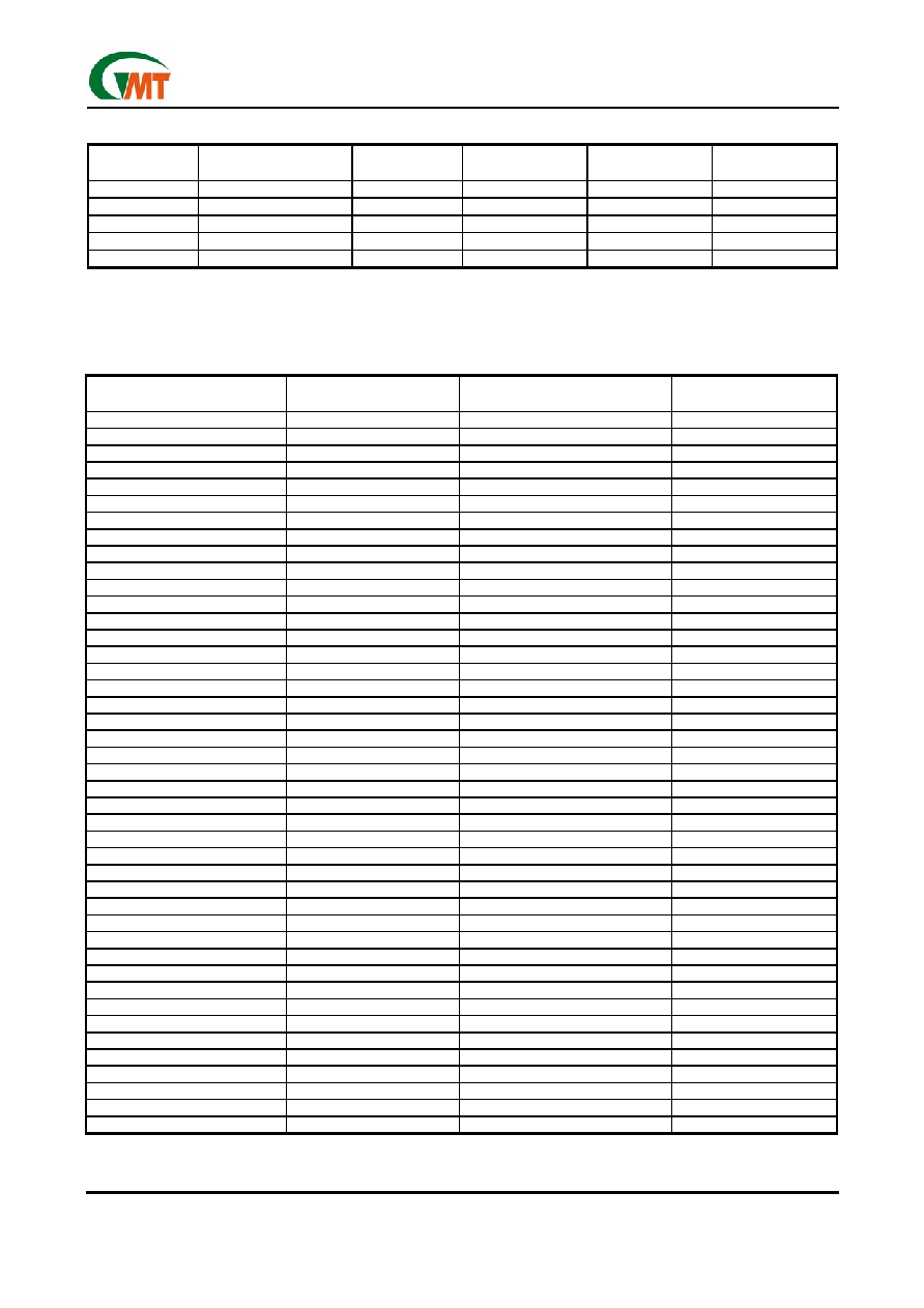
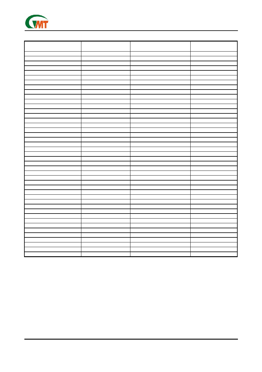
Ordering Information
ORDER
NUMBER
ORDER NUMBER
(Pb free)
MARKING VOLTAGE
TEMP.
RANGE
PACKAGE
G916-250TOU G916-250TOUf
96ANx
2.50V
-40∞C~ +85∞C
TSOT-23-5
G916-270TOU G916-270TOUf
96APx
2.70V
-40∞C~ +85∞C
TSOT-23-5
G916T1U G916T1Uf
16xx Adjustable
-40∞C~ +85∞C
SOT-23-5
G916-120T1U G916-120T1Uf
96AAx
1.20V -40∞C~ +85∞C
SOT-23-5
G916-330T1U G916-330T1Uf
6Axx
3.30V -40∞C~ +85∞C
SOT-23-5
For other output voltage, please contact us at sales
@
gmt.com.tw
Note:
TO: TSOT-23-5 T1: SOT-23-5
U: Tape & Reel
Selector Guide
ORDER NUMBER
ORDER NUMBER
(Pb free)
OUTPUT VOLTAGE (V)
MARKING
G916TOU G916TOUf Adjustable
16xx
G916-120TOU G916-120TOUf
1.20
96AAx
G916-130TOU G916-130TOUf
1.30
96ABx
G916-140TOU G916-140TOUf
1.40
96ACx
G916-150TOU G916-150TOUf
1.50
96ADx
G916-160TOU G916-160TOUf
1.60
96AEx
G916-170TOU G916-170TOUf
1.70
96AFx
G916-180TOU G916-180TOUf
1.80
96AGx
G916-190TOU G916-190TOUf
1.90
96AHx
G916-200TOU G916-200TOUf
2.00
96AIx
G916-210TOU G916-210TOUf
2.10
96AJx
G916-220TOU G916-220TOUf
2.20
96AKx
G916-230TOU G916-230TOUf
2.30
96ALx
G916-240TOU G916-240TOUf
2.40
96AMx
G916-250TOU G916-250TOUf
2.50
96ANx
G916-260TOU G916-260TOUf
2.60
96AOx
G916-270TOU G916-270TOUf
2.70
96APx
G916-280TOU G916-280TOUf
2.80
96AQx
G916-285TOU G916-285TOUf
2.85
96ARx
G916-290TOU G916-290TOUf
2.90
96ASx
G916-300TOU G916-300TOUf
3.00
96ATx
G916-310TOU G916-310TOUf
3.10
96AUx
G916-315TOU G916-315TOUf
3.15
96AVx
G916-320TOU G916-320TOUf
3.20
96AWx
G916-330TOU G916-330TOUf
3.30
6Axx
G916-340TOU G916-340TOUf
3.40
96AYx
G916-350TOU G916-350TOUf
3.50
96AZx
G916-360TOU G916-360TOUf
3.60
96BAx
G916-370TOU G916-370TOUf
3.70
96BBx
G916-380TOU G916-380TOUf
3.80
96BCx
G916-390TOU G916-390TOUf
3.90
96BDx
G916-400TOU G916-400TOUf
4.00
96BEx
G916-410TOU G916-410TOUf
4.10
96BFx
G916-420TOU G916-420TOUf
4.20
96BGx
G916-430TOU G916-430TOUf
4.30
96BHx
G916-440TOU G916-440TOUf
4.40
96BIx
G916-450TOU G916-450TOUf
4.50
96BJx
G916-460TOU G916-460TOUf
4.60
96BKx
G916-470TOU G916-470TOUf
4.70
96BLx
G916-475TOU G916-475TOUf
4.75
96BMx
G916-480TOU G916-480TOUf
4.80
96BNx
G916-490TOU G916-490TOUf
4.90
96BOx
G916-500TOU G916-500TOUf
5.00
96BPx
TO: TSOT-23-5
Ver: 1.7
Jan 25, 2006
TEL: 886-3-5788833
http://www.gmt.com.tw
3
G916
Global Mixed-mode Technology Inc.
Selector Guide
ORDER NUMBER
ORDER NUMBER
(Pb free)
OUTPUT VOLTAGE (V)
MARKING
G916T1U G916T1Uf Adjustable
16xx
G916-120T1U G916-120T1Uf
1.20
96AAx
G916-130T1U G916-130T1Uf
1.30
96ABx
G916-140T1U G916-140T1Uf
1.40
96ACx
G916-150T1U G916-150T1Uf
1.50
96ADx
G916-160T1U G916-160T1Uf
1.60
96AEx
G916-170T1U G916-170T1Uf
1.70
96AFx
G916-180T1U G916-180T1Uf
1.80
96AGx
G916-190T1U G916-190T1Uf
1.90
96AHx
G916-200T1U G916-200T1Uf
2.00
96AIx
G916-210T1U G916-210T1Uf
2.10
96AJx
G916-220T1U G916-220T1Uf
2.20
96AKx
G916-230T1U G916-230T1Uf
2.30
96ALx
G916-240T1U G916-240T1Uf
2.40
96AMx
G916-250T1U G916-250T1Uf
2.50
96ANx
G916-260T1U G916-260T1Uf
2.60
96AOx
G916-270T1U G916-270T1Uf
2.70
96APx
G916-280T1U G916-280T1Uf
2.80
96AQx
G916-285T1U G916-285T1Uf
2.85
96ARx
G916-290T1U G916-290T1Uf
2.90
96ASx
G916-300T1U G916-300T1Uf
3.00
96ATx
G916-310T1U G916-310T1Uf
3.10
96AUx
G916-315T1U G916-315T1Uf
3.15
96AVx
G916-320T1U G916-320T1Uf
3.20
96AWx
G916-330T1U G916-330T1Uf
3.30
6Axx
G916-340T1U G916-340T1Uf
3.40
96AYx
G916-350T1U G916-350T1Uf
3.50
96AZx
G916-360T1U G916-360T1Uf
3.60
96BAx
G916-370T1U G916-370T1Uf
3.70
96BBx
G916-380T1U G916-380T1Uf
3.80
96BCx
G916-390T1U G916-390T1Uf
3.90
96BDx
G916-400T1U G916-400T1Uf
4.00
96BEx
G916-410T1U G916-410T1Uf
4.10
96BFx
G916-420T1U G916-420T1Uf
4.20
96BGx
G916-430T1U G916-430T1Uf
4.30
96BHx
G916-440T1U G916-440T1Uf
4.40
96BIx
G916-450T1U G916-450T1Uf
4.50
96BJx
G916-460T1U G916-460T1Uf
4.60
96BKx
G916-470T1U G916-470T1Uf
4.70
96BLx
G916-475T1U G916-475T1Uf
4.75
96BMx
G916-480T1U G916-480T1Uf
4.80
96BNx
G916-490T1U G916-490T1Uf
4.90
96BOx
G916-500T1U G916-500T1Uf
5.00
96BPx
T1: SOT-23-5

Ver: 1.7
Jan 25, 2006
TEL: 886-3-5788833
http://www.gmt.com.tw
4
G916
Global Mixed-mode Technology Inc.
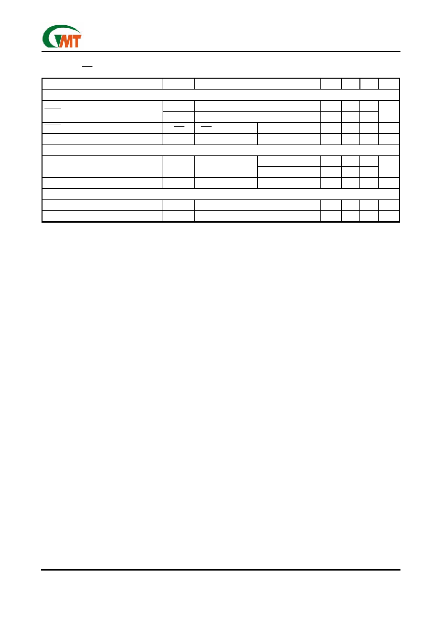
Absolute Maximum Ratings
IN to GND. . . . . . . . . . . . . . . . . . . . . . . . -0.3V to 7V
Output Short-Circuit Duration . . . . . . . . . . . . .Infinite
SET, BYP to GND . . . . . . . . . . . . . . . . . -0.3V to 7V
SHDN
to GND . . . . . . . . . . . . . . . . . . .-0.3V to 7V
SHDN
to IN . . . . . . . . . . . . . . . . . . . . .-7V to 0.3V
OUT to GND . . . . . . . . . . . . . ..-0.3V to (V
IN
+ 0.3V)
Operating Temperature Range . . . . . . .-40∞C to 85∞C
Junction Temperature . . . . . . . . . . . . . . . . . . . . . 150∞C
Thermal Resistance Junction to Ambient, (
JA
)
SOT-23-5. . . . . . . . . . . . . . . . . . . . . . . . . . . . 240∞C/W
(1)
TSOT-23-5 . . . . . . . . . . . . . . . . . . . . . . . . . . . .196∞C/W
Storage Temperature Range . . . . . . . . .-65∞C to 160∞C
Reflow Temperature (soldering, 10sec) . . . . . . . .260∞C
Note
(1)
: See Recommended Minimum Footprint
Stresses beyond those listed under "Absolute Maximum Ratings" may cause permanent damage to the device. These are stress ratings
only and functional operation of the device at these or any other conditions beyond those indicated in the operational sections of the
specifications is not implied. Exposure to absolute maximum rating conditions for extended periods may affect device reliability.
Electrical Characteristics
(V
IN
=3.6V, V
SHDN
=V
IN
, T
A
=25
∞
C, unless otherwise noted.) (Note 1)
PARAMETER SYMBOL
CONDITION MIN
TYP
MAX UNIT
Input Voltage (Note 2)
V
IN
2.5
---
6.0
V
Output Voltage Accuracy (adjustable mode)
V
OUT
Variation from specified V
OUT
, I
OUT
=1mA -2 --- 2 %
V
OUT
2.50V, I
OUT
=1mA
-2 --- 2
2.50V>V
OUT
1.80V, I
OUT
=1mA
-3 --- 3
Output Voltage Accuracy (fixed mode)
V
OUT
1.80V>V
OUT
1.20V, I
OUT
=1mA
-4 --- 4
%
Adjustable Output Voltage Range (Note 3)
V
OUT
V
SET
--- 5.5
V
Maximum Output Current
300
---
---
mA
Current Limit (Note 4)
I
LIM
400
550
---
mA
Short Circuit Current
Isc
---
280
---
mA
Ground Pin Current
I
Q
--- 90 ---
µA
V
OUT
=1.50V ---
1.36
1.7
V
OUT
=1.80V ---
1.10
1.4
V
OUT
=2.50V ---
0.58
0.8
V
OUT
=3.00V ---
0.41
0.5
V
OUT
=3.30V ---
0.36
0.5
V
OUT
=4.75V ---
0.25
0.5
Dropout Voltage (Note 5)
V
DROP
I
OUT
=300mA
V
OUT
=5.00V ---
0.24
0.5
V
Line Regulation
V
LNR
SET=GND, V
IN
=V
(STD)
+0.1V to 6.2V
I
OUT
=10mA
--- 0.06
0.12
%/V
Load Regulation
V
LDR
I
OUT
=10mA to 300mA
---
--- 0.02 %/mA
Ripple Rejection
PSRR F=120Hz, 0.45V
P-P
, I
OUT
=10mA ---
65
---
dB
Output Voltage Noise (10Hz to 100kHz)
e
n
C
OUT
=1µF, I
OUT
=1mA, C
BYP
=10nF
--- 28 ---
µV
RMS
Ver: 1.7
Jan 25, 2006
TEL: 886-3-5788833
http://www.gmt.com.tw
5
G916
Global Mixed-mode Technology Inc.
Electrical Characteristics
(continued)
(V
IN
=3.6V, V
SHDN
=V
IN
, T
A
=25
∞
C, unless otherwise noted.) (Note 1)
PARAMETER SYMBOL
CONDITION MIN
TYP
MAX UNIT
SHUTDOWN
V
IH
Regulator
enabled
1.5 --- ---
SHDN
Input Threshold
V
IL
Regulator
shutdown
--- --- 0.4
V
SHDN
Input Bias Current
I
SHDN
V
SHDN
= V
IN
T
A
= +25∞C
--- 0.003 0.1
µA
Shutdown Supply Current
I
QSHDN
V
OUT
= 0V
T
A
= +25∞C
--- 0.2 1 µA
SET INPUT
T
A
= +25∞C
1.225 1.25 1.275
SET Reference Voltage (Note 3)
V
SET
V
IN
= 2.5V to 5.5V,
I
OUT
= 1mA
T
A
= T
MIN
to T
MAX
--- 1.25 ---
V
SET Input Leakage Current (Note 3)
I
SET
V
SET
= 1.3V
T
A
= +25∞C ---
5
30
nA
THERMAL PROTECTION
Thermal Shutdown Temperature
T
SHDN
--- 145 ---
∞C
Thermal Shutdown Hysteresis
T
SHDN
---
25
---
∞C
Note 1: Limits is 100% production tested at T
A
= +25∞C. Low duty pulse techniques are used during test to maintain junc-
tion temperature as close to ambient as possible.
Note 2: Guaranteed by line regulation test.
Note 3: Adjustable mode only.
Note 4: Not tested. For design purposes, the current limit should be considered 400mA minimum to 650mA maximum.
Note 5: The dropout voltage is defined as (V
IN
-V
OUT
) when V
OUT
is 100mV below the target value of V
OUT
. The performance of
every G916 part, see "Typical Performance Characteristics".
Ver: 1.7
Jan 25, 2006
TEL: 886-3-5788833
http://www.gmt.com.tw
6
G916
Global Mixed-mode Technology Inc.
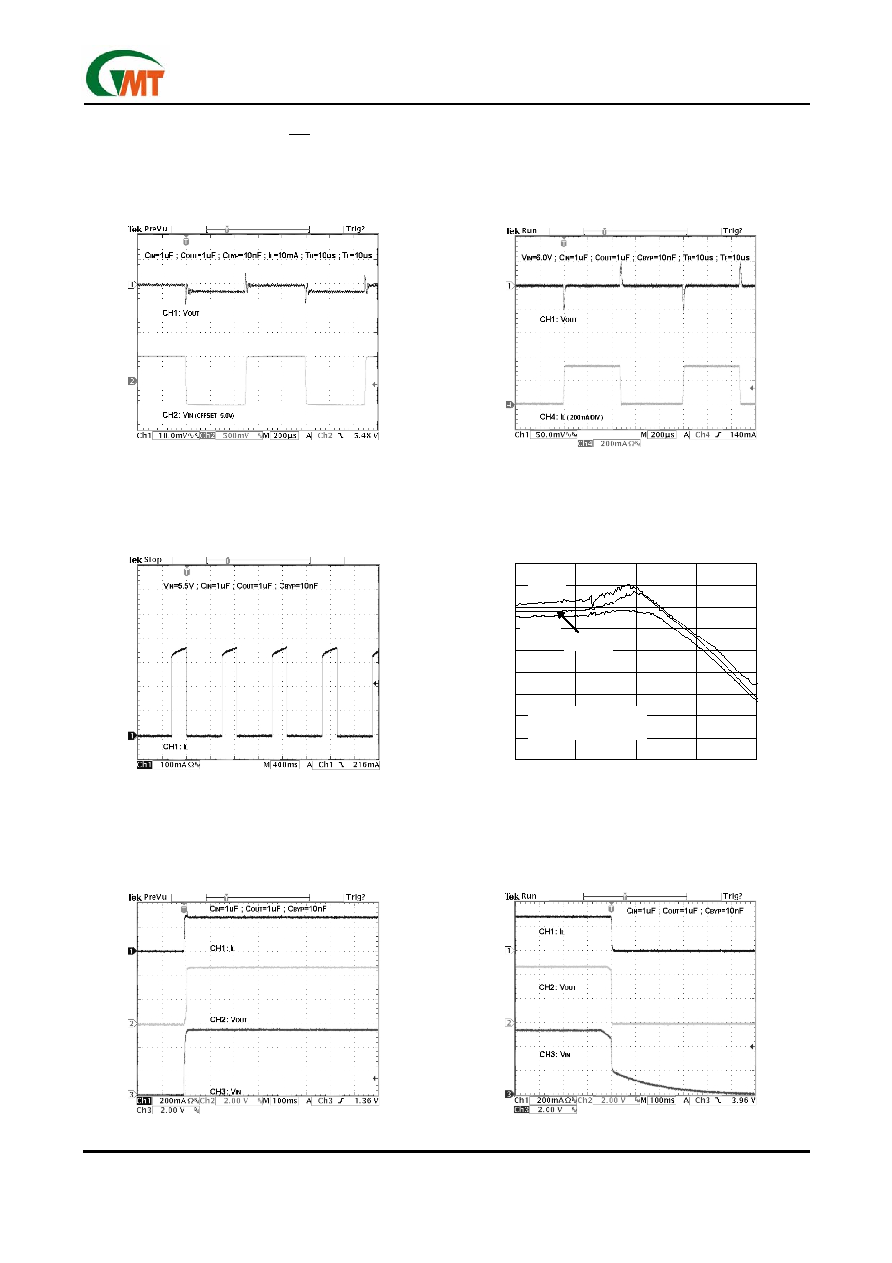
Typical Performance Characteristics
(V
IN
=5V, C
IN
=1
µ
F, C
OUT
=1
µ
F, V
SHDN
= V
IN
, G916-475, T
A
=25
∞
C, unless otherwise noted.)
Short Circuit Current
Turn-On
Turn-Off
Line Transient
Load Transient
0
10
20
30
40
50
60
70
80
90
0.01
0.1
1
10
100
Frequency (KHz)
PS
R
R
(
d
B)
V
IN
=4V ; COUT=1µF ;
C
BYP
=10nF ; V
r
=245mV
300mA
100mA
10mA
Ripple Rejection

Ver: 1.7
Jan 25, 2006
TEL: 886-3-5788833
http://www.gmt.com.tw
7
G916
Global Mixed-mode Technology Inc.
Typical Performance Characteristics
(continued)
4.2
4.3
4.4
4.5
4.6
4.7
4.8
4.9
5.0
5.1
5.2
-25 -15 -5 5 15 25 35 45 55 65 75 85
Temperature (∞C)
O
u
tpu
t
V
o
l
t
ag
e
(
V
)
0
50
100
150
200
250
300
0
50
100
150
200
250
300
I
L
(mA)
D
r
op
ou
t
V
o
l
t
age
(
m
V
)
T
A
=85∞C
V
IN
=5.0V
V
IN
=5.5V
I
L
=10mA
Overcurrent Protection Characteristics
Dropout Voltage vs. I
L
T
A
=25∞C
T
A
=-25∞C
Output Voltage vs. Temperature
Output Noise
Ver: 1.7
Jan 25, 2006
TEL: 886-3-5788833
http://www.gmt.com.tw
8
G916
Global Mixed-mode Technology Inc.
Pin Description
PIN
G916
G916-XXX
NAME
FUNCTION
1
1
IN
Regulator Input. Supply voltage can range from +2.5V to +6.0V. Bypass with 1µF to GND
2 2
GND
Ground. This pin also functions as a heatsink. Solder to large pads or the circuit board
ground plane to maximize thermal dissipation.
3 3
SHDN
Active-Low Shutdown Input. A logic low reduces the supply current to less than 1µA. Connect to IN
for normal operation.
4
SET
Feedback Input for Setting the Output Voltage. Connect to GND to set the output voltage to
the preset output voltage. Connect to an external resistor divider for adjustable-output op-
eration.
4
BYP
This is a reference bypass pin. It should connect external 10nF capacitor to GND to reduce
output noise. Bypass capacitor must be no less than 1nF. (C
BYP
1nF)
5 5
OUT
Regulator Output. Sources up to 300mA. Bypass with a 1µF, 0.2
typical ESR capacitor
to GND.
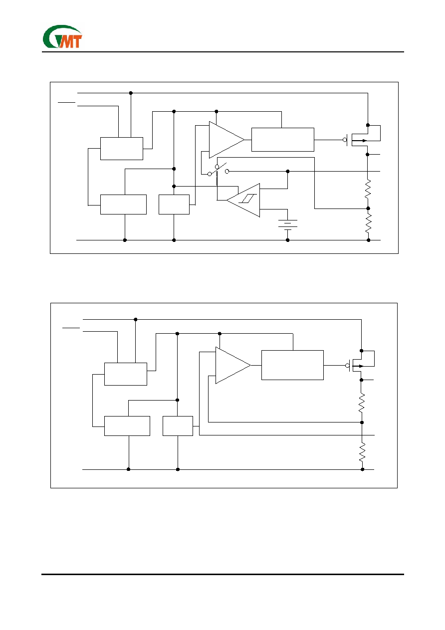
Detailed Description
The block diagram of the G916 is shown in Figure 1. It
consists of an error amplifier, 1.25V bandgap reference,
PMOS output transistor, internal feedback voltage divider,
mode comparator, shutdown logic, over current protec-
tion circuit, and over temperature protection circuit.
The mode comparator compares the SET pin voltage
with an internal 350mV reference. If the SET pin volt-
age is less than 350mV, the internal feedback voltage
divider's central tap is connected to the non-inverting
input of the error amplifier. The error amplifier com-
pares non-inverting input with the 1.25V bandgap ref-
erence. If the feedback voltage is higher than 1.25V,
the error amplifier's output becomes higher so that the
PMOS output transistor has a smaller gate-to-source
voltage (V
GS
). This reduces the current carrying capa-
bility of the PMOS output transistor, as a result the
output voltage decreases until the feedback voltage is
equal to 1.25V. Similarly, when the feedback voltage is
less than 1.25V, the error amplifier causes the output
PMOS to source more current to pull the feedback
voltage up to 1.25V. Thus, through this feedback ac-
tion, the error amplifier, output PMOS, and the voltage
dividers effectively form a unity-gain amplifier with the
feedback voltage force to be the same as the 1.25V
bandgap reference. The output voltage, V
OUT
, is then
given by the following equation:
V
OUT
= 1.25 (1 + R1/R2). (1)
Alternatively, the relationship between R1 and R2 is
given by:
R1 = R2 (V
OUT
/1.25 - 1).
(2)
For the reasons of reducing power dissipation and
loop stability, R2 is chosen to be 100K
. For G916,
R1 is 164K, and the pre-set VOUT is 3.30V.
When external voltage divider is used, as shown in
Figure 2, the SET pin voltage will be larger than
350mV. The non-inverting input of the amplifier will be
connected to the external voltage divider. However,
the operation of the feedback loop is the same, so that
the conditions of Equations 1 and 2 are still true. The
output voltage is still given by Equation 1.
For G916-XXX, adjust the internal reference and in-
ternal voltage divider. It provides a fixed mode output
ranging from 1.2V to 5V.
Ver: 1.7
Jan 25, 2006
TEL: 886-3-5788833
http://www.gmt.com.tw
9
G916
Global Mixed-mode Technology Inc.
Figure 1. Functional Diagram of Adjustable-mode & Fixed mode
SHDN
IN
OUT
SHUTDOWN
LOGIC
1.25V
Vref
ERROR
AMP
OVER CURRENT
PROTECT & DYNAMIC
FEEDBACK
GND
350mV
SET
R1
R2
OVER TEMP.
PROTECT
P
MODE COMPARATOR
SHDN
IN
OUT
SHUTDOWN
LOGIC
1.25V
Vref
ERROR
AMP
OVER CURRENT
PROTECT & DYNAMIC
FEEDBACK
GND
350mV
SET
R1
R2
OVER TEMP.
PROTECT
P
MODE COMPARATOR
SHDN
IN
OUT
SHUTDOWN
LOGIC
1.25V
Vref
ERROR
AMP
OVER CURRENT
PROTECT & DYNAMIC
FEEDBACK
GND
R1
R2
OVER TEMP.
PROTECT
BYP
P
SHDN
IN
OUT
SHUTDOWN
LOGIC
1.25V
Vref
ERROR
AMP
OVER CURRENT
PROTECT & DYNAMIC
FEEDBACK
GND
R1
R2
OVER TEMP.
PROTECT
BYP
SHDN
IN
OUT
SHUTDOWN
LOGIC
1.25V
Vref
ERROR
AMP
OVER CURRENT
PROTECT & DYNAMIC
FEEDBACK
GND
R1
R2
OVER TEMP.
PROTECT
BYP
P

Ver: 1.7
Jan 25, 2006
TEL: 886-3-5788833
http://www.gmt.com.tw
10
G916
Global Mixed-mode Technology Inc.
Figure 2. Adjustable Output Using External
Feedback Resistors
Over Current Protection
The G916 uses a current sense-resistor to monitor the
output current. A portion of the PMOS output transis-
tor's current is mirrored to a resistor such that the
voltage across this resistor is proportional to the output
current. Once the output current exceeds limit thresh-
old, G916 would be protected with a limited output
current. Further more, when the output is short to
ground, the output current would be folded-back to a
less limit.
Over Temperature Protection
To prevent abnormal temperature from occurring, the
G916 has a built-in temperature monitoring circuit.
When it detects the temperature is above 145∞C, the
output transistor is turned off. When the IC is cooled
down to below 120∞C, the output is turned on again. In
this way, the G916 will be protected against abnormal
junction temperature during operation.
Shutdown Mode
When the
SHDN
pin is connected a logic low voltage,
the G916 enters shutdown mode. All the analog cir-
cuits are turned off completely, which reduces the
current consumption to only the leakage current. The
G916 output pass transistor would get into high im-
pedance level. There is an internal discharge path to
help to shorten discharge delay time.
Operating Region and Power Dissipation
Since the G916 is a linear regulator, its power dissipa-
tion is always given by P = I
OUT
(V
IN
≠ V
OUT
). The
maximum power dissipation is given by:
P
D(MAX)
= (T
J
≠T
A
) /
JA
,=(150∞C-25∞C)/240∞C/W = 520mW
Where (T
J
≠T
A
) is the temperature difference the G916
die and the ambient air,
JA
, is the thermal resistance
of the chosen package to the ambient air. For surface
mount device, heat sinking is accomplished by using
the heat spreading capabilities of the PC board and its
copper traces. In the case of a SOT-23-5 package, the
thermal resistance is typically 240∞C/Watt. (See Rec-
ommended Minimum Footprint). Refer to Figure 3a &
3b is the G916 valid operating region (Safe Operating
Area) & refer to Figure 4 is maximum power dissipa-
tion of SOT-23-5.
The die attachment area of the G916's lead frame is
connected to pin 2, which is the GND pin. Therefore,
the GND pin of G916 can carry away the heat of the
G916 die very effectively. To improve the maximum
power providing capability, connect the GND pin to
ground using a large ground plane near the GND pin.
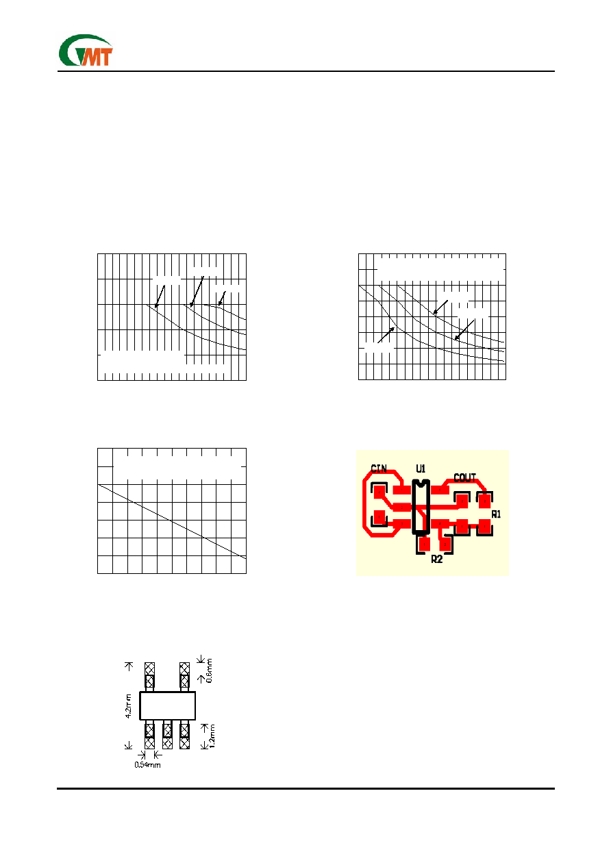
Applications Information
Capacitor Selection and Regulator Stability
Normally, use a 1µF capacitor on the input and a 1µF
capacitor on the output of the G916. Larger input ca-
pacitor values and lower ESR provide better sup-
ply-noise rejection and transient response. A higher-
value input capacitor (10µF) may be necessary if large,
fast transients are anticipated and the device is lo-
cated several inches from the power source.
Power-Supply Rejection and Operation from
Sources Other than Batteries
The G916 is designed to deliver low dropout voltages
and low quiescent currents in battery powered sys-
tems. Power-supply rejection is 65dB at low frequen-
cies. As the frequency increases above 20kHz, the
output capacitor is the major contributor to the rejec-
tion of power-supply noise.
When operating from sources other than batteries,
improve supply-noise rejection and transient response
by increasing the values of the input and output ca-
pacitors, and using passive filtering techniques.
Load Transient Considerations
The G916 load-transient response graphs show two
components of the output response: a DC shift of the
output voltage due to the different load currents, and
the transient response. Typical overshoot for step
changes in the load current from 10mA to 300mA is
8mV. Increasing the output capacitor's value and de-
creasing its ESR attenuates transient spikes.
Input-Output (Dropout) Voltage
A regulator's minimum input-output voltage differential
(or dropout voltage) determines the lowest usable sup-
ply voltage. In battery-powered systems, this will de-
termine the useful end-of-life battery voltage. Because
the G916 use a P-channel MOSFET pass transistor,
their dropout voltage is a function of R
DS(ON)
multiplied
by the load current.
IN
OUT
SET
SHDN
G916
BATTERY C
IN
1µF
R1
R2
C
OUT
1µF
R
L
OUTPUT
VOLTAGE
GND
IN
OUT
SET
SHDN
G916
BATTERY C
IN
1µF
R1
R2
C
OUT
1µF
R
L
OUTPUT
VOLTAGE
GND
Ver: 1.7
Jan 25, 2006
TEL: 886-3-5788833
http://www.gmt.com.tw
11
G916
Global Mixed-mode Technology Inc.
Layout Guide
An input capacitance of
1µF is required between the
G916 input pin and ground (the amount of the capaci-
tance may be increased without limit), This capacitor
must be located a distance of not more than 1cm from
the input and return to a clean analog ground.
Input capacitor can filter out the input voltage spike
caused by the surge current due to the inductive effect
of the package pin and the printed circuit board's rout-
ing wire. Otherwise, the actual voltage at the IN pin
may exceed the absolute maximum rating.
The output capacitor also must be located a distance
of not more than 1cm from output to a clean analog
ground. Because it can filter out the output spike
caused by the surge current due to the inductive effect
of the package pin and the printed circuit board's rout-
ing wire. Figure 5 is adjustable mode of G916 PCB
layout.
0
50
100
150
200
250
300
350
400
0.5 0.7 0.9 1.1 1.3 1.5 1.7 1.9 2.1 2.3 2.5 2.7 2.9 3.1 3.3 3.5 3.7 3.9 4.1 4.3
Input-Output Voltage Differential V
IN
-V
OUT
(V)
O
u
tp
ut
Cu
r
r
en
t I
OUT
(mA
)
T
A
= 85∞C
Still air
1oz copper on SOT-23-5 package
Mounted on recommended foorprint (R
JA
=240∞C/W)
T
A
= 25∞C
T
A
= 55∞C
Note: V
IN
(max) <= 5.5V
0
0.1
0.2
0.3
0.4
0.5
0.6
0.7
25
35
45
55
65
75
85
95
105
115
125
Amibent Temperature T
A
(∞C)
Pow
e
r Di
s
s
i
pati
on P
D
(W)
Still air
1oz copper on SOT-23-5 package
Mounted on recommended foorprint (R
JA
=240∞C/W)
0
50
100
150
200
250
0.2 0.4 0.6 0.8 1.0 1.2 1.4 1.6 1.8 2.0 2.2 2.4 2.6 2.8 3.0 3.2 3.4 3.6 3.8 4.0 4.2
Input-Output Voltage Differential V
IN
-V
OUT
(V)
O
u
tput
Cur
r
ent
I
OUT
(m
A
)
Mounted on recommended foorprint (R
JA
=240∞C/W)
T
A
= 25∞C
T
A
= 55
∞C
T
A
= 85∞C
Still Air
1oz copper on SOT-23-5 Package
Recommend Minimum Footprint
TSOT-23-5
SOT-23-5
Figure 5. Adjustable Mode
*Distance between pin & capacitor must no more than 1cm
Figure 3a. Safe Operating Area (I
OUT
=150mA)
Safe Operating Area of I
OUT
=150mA
[Power Dissipation Limit]
Note: V
IN
(max) <= 5.5V
Maximum Power Dissipation of SOT-23-5
Figure 4. Power Dissipation vs. Ambient Temperature
Figure 3b. Safe Operating Area (I
OUT
=300mA)
Safe Operating Area of I
OUT
=300mA
[Power Dissipation Limit]

Ver: 1.7
Jan 25, 2006
TEL: 886-3-5788833
http://www.gmt.com.tw
12
G916
Global Mixed-mode Technology Inc.
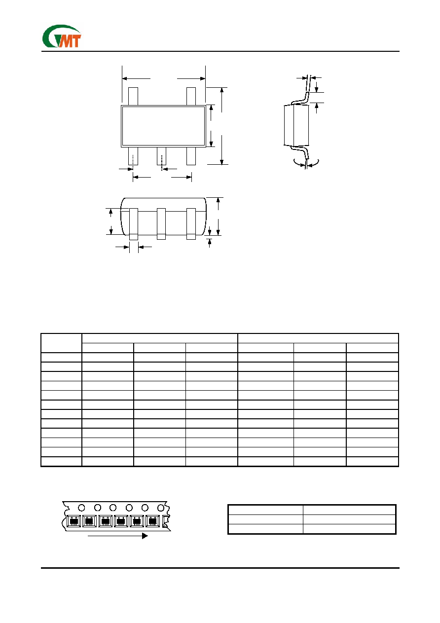
Package Information
TSOT-23-5 Package
Note:
1. Package body sizes exclude mold flash protrusions or gate burrs
2. Tolerance ±0.1000 mm (4mil) unless otherwise specified
3. Coplanarity: 0.1000mm
4.
Dimension L is measured in gage plane
DIMENSION IN MM
DIMENSION IN INCH
SYMBOL
MIN. NOM. MAX. MIN. NOM. MAX.
A ----- ----- 1.00 ----- ----- 0.039
A1 0.00 ----- 0.10 0.000 ----- 0.004
A2 ----- ----- 0.90 ----- ----- 0.035
b 0.35 0.40 0.50 0.014 0.016 0.020
C 0.10 0.15 0.25 0.004 0.006 0.010
D 2.70 2.90 3.10 0.106 0.114 0.122
E 1.40 1.60 1.80 0.055 0.063 0.071
e -----
1.90(TYP)
----- -----
0.075(TYP)
-----
e1 ----- 0.95 ----- ----- 0.037 -----
H 2.60 2.80 3.00 0.102 0.110 0.118
L 0.37 ------ ----- 0.015 ----- -----
1
1∞
5∞
9∞
1∞
5∞
9∞
E
e
D
H
1
L
C
b
A2
A1
A
e1
E
e
D
H
1
L
C
b
A2
A1
A
e1
Ver: 1.7
Jan 25, 2006
TEL: 886-3-5788833
http://www.gmt.com.tw
13
G916
Global Mixed-mode Technology Inc.
SOT-23-5 Package
Note:
1. Package body sizes exclude mold flash protrusions or gate burrs
2. Tolerance
±0.1000 mm (4mil) unless otherwise specified
3. Coplanarity:
0.1000mm
4.
Dimension L is measured in gage plane
DIMENSION IN MM
DIMENSION IN INCH
SYMBOL
MIN. NOM. MAX. MIN. NOM. MAX.
A 1.00 1.10 1.30 0.039 0.043 0.051
A1 0.00 ----- 0.10 0.000 ----- 0.004
A2 0.70 0.80 0.90 0.028 0.031 0.035
b 0.35 0.40 0.50 0.014 0.016 0.020
C 0.10 0.15 0.25 0.004 0.006 0.010
D 2.70 2.90 3.10 0.106 0.114 0.122
E 1.40 1.60 1.80 0.055 0.063 0.071
e -----
1.90(TYP)
----- -----
0.075(TYP)
-----
e1 ----- 0.95 ----- ----- 0.037 -----
H 2.60 2.80 3.00 0.102 0.110 0.118
L 0.37 ------ ----- 0.015 ----- -----
1
1∞
5∞
9∞
1∞
5∞
9∞
Taping Specification
PACKAGE Q
'
TY/REEL
TSOT-23-5 3,000
ea
SOT-23-5 3,000
ea
GMT Inc. does not assume any responsibility for use of any circuitry described, no circuit patent licenses are implied and GMT Inc. reserves the right at any time without notice to change said circuitry and specifications.
E
e
D
H
1
L
C
b
A2
A1
A
e1
E
e
D
H
1
L
C
b
A2
A1
A
e1
Feed Direction
TSOT-23-5
SOT-23-5 Package Orientation
Feed Direction
TSOT-23-5
SOT-23-5 Package Orientation