 | –≠–ª–µ–∫—Ç—Ä–æ–Ω–Ω—ã–π –∫–æ–º–ø–æ–Ω–µ–Ω—Ç: G930T81B | –°–∫–∞—á–∞—Ç—å:  PDF PDF  ZIP ZIP |
Ver: 4.5
May 13, 2002
TEL: 886-3-5788833
http://www.gmt.com.tw
1
G930/G931
Global Mixed-mode Technology Inc.
3.5V 400mA Low Dropout Regulator
Features
Dropout voltage typically 0.8V @ I
O
= 400mA
Output current in excess of 400mA
Output voltage accuracy +3%/-2%
Quiescent current, typically 600
µ
µ
µ
µA
Internal short circuit current limit
Internal over temperature protection
General Description
The G930/G931 positive 3.5V voltage regulator fea-
tures the ability to source 400mA of output current
with a dropout voltage of typically 0.8V over the en-
tire operating temperature range. A low quiescent
current is provided over the entire output current
range. The typical quiescent current is 0.6mA. Fur-
thermore, the quiescent current is smaller when the
regulator is in the dropout mode (V
IN
< 3.5V).
Familiar regulator features such as over temperature
and over current protection circuits are provided to
prevent it from being damaged by abnormal operating
conditions.
Ordering Information
PIN OPTION
ORDER NUMBER
PACKAGE TYPE
1 2 3
G930T21U SOT
89
V
OUT
GND V
IN
G931T24U SOT
89
GND
V
IN
V
OUT
* For other package types, pin options and package, please contact us at sales @gmt.com.tw
Order Number Identification
GXXX XX X X
Packing Type
Pin Option
Package Type
Part Number
PACKAGE TYPE
PIN OPTION
PACKING
T2 : SOT 89
1
2
3
U & D : Tape & Reel Direction
T6 : SOT 223
1 : V
OUT
GND V
IN
T : Tube
T7 : SOT 23
2 : V
OUT
V
IN
GND
B : Bag
T8 : µTO92
3 : GND
V
OUT
V
IN
4 : GND
V
IN
V
OUT
5 : V
IN
GND
V
OUT
6 : V
IN
V
OUT
GND
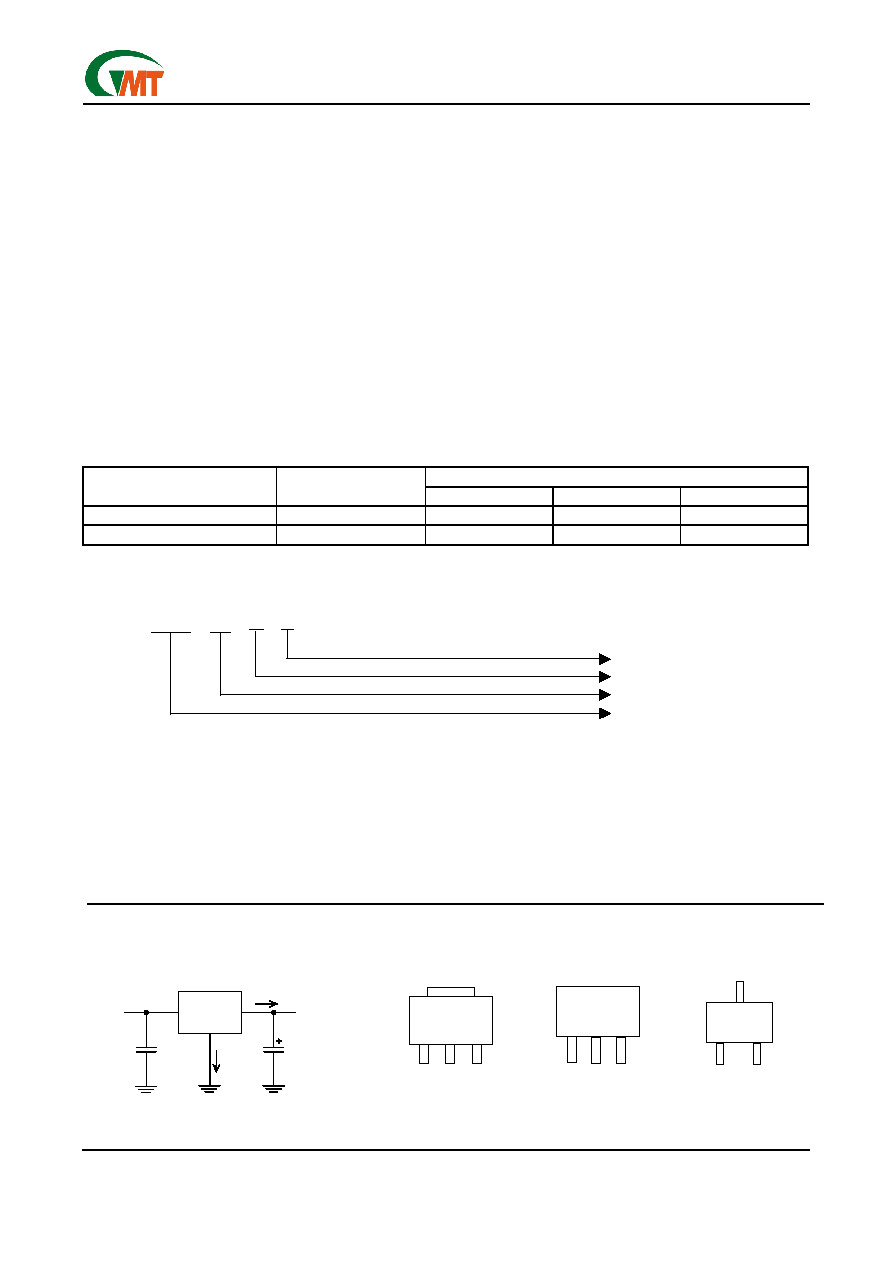
Typical Application Package Type
[Note 4] : Type of C
OUT
Top View
1
2
3
Top View
1
3
µTO 92
Top View
SOT 23
1
3
2
Top View
Top View
1
2
3
SOT 89223
Top View
2
V
IN
G930
C1
0.47µF
IQ
V
OUT
I
O
C
OUT
10µF
Top View
Top View
1
2
3
Top View
1
3
µTO 92
Top View
SOT 23
1
3
2
Top View
Top View
1
2
3
SOT 89223
Top View
2
V
IN
G930
C1
0.47µF
IQ
V
OUT
I
O
C
OUT
10µF
Ver: 4.5
May 13, 2002
TEL: 886-3-5788833
http://www.gmt.com.tw
2
G930/G931
Global Mixed-mode Technology Inc.
Absolute Maximum Ratings
(Note 1)
Input Voltage...................................................10V
Power Dissipation Internally Limited (Note 2)
Maximum Junction Temperature...........................150∞C
Storage Temperature Range..........-65∞C
T
J
+150∞C
Lead Temperature, Time for Wave Soldering
SOT-89 Package......................................260∞C, 4s
Continuous Power Dissipation (T
A
= +25∞C)
SOT89
(1)
:....................................................0.42W
Note
(1)
:See Recommended Minimum Footprint.
Operating Conditions
(Note 1)
Input Voltage..............................................4V~7V
Temperature Range........................0∞C
T
J
125∞C
Electrical Characteristics
V
IN
=5V, I
O
= 400mA, C
IN
= 1µF, C
OUT
=10 µF, All specifications apply for T
A
= T
J
= 25∞C. [Note 3]
PARAMETER CONDITIONS MIN
TYP
MAX
UNITS
Output Voltage
5mA < I
O
<400mA 3.43
3.5
3.605
V
Line Regulation
4V < V
IN
< 7V, I
O
= 10mA
22
mV
Load Regulation
50mA < I
O
<
400mA
30 mV
Output Impedance
100mA DC and 100mA AC, fo = 120Hz
103
m
Quiescent Current
V
IN
=
5V
0.6 mA
Ripple Rejection
f
i
= 120Hz, 1V
P-P
,
Io = 100mA
42
dB
I
O
= 400mA
0.8
0.9
V
Dropout Voltage
I
O
= 100mA
125
150
mV
Short Circuit Current
0.77
A
Over Temperature
125
∞C
Note 1: Absolute Maximum Ratings are limits beyond which damage to the device may occur. Operating
Conditions are conditions under which the device functions but the specifications might not be guaranteed. For
guaranteed specifications and test conditions see the Electrical Characteristics.
Note 2: The maximum power dissipation is a function of the maximum junction temperature, T
Jmax
; total thermal re-
sistance,
JA
, and ambient temperature T
A
. The maximum allowable power dissipation at any ambient tem-
perature is T
jmax
-T
A
/
JA
. If this dissipation is exceeded, the die temperature will rise above 130∞C and IC
will go into thermal shutdown. For the G930/G931 in SOT 89 package,
JA
is 250∞C/W. (See Recom-
mended Minimum Footprint). The safe operation in SOT 89, it can see "Typical Performance Characteris-
tics" (Safe Operating Area).
Note3: Low duty pulse techniques are used during test to maintain junction temperature as close to ambient as pos-
sible.
Note4: The type of output capacitor should be tantalum or aluminum.
Definitions
Dropout Voltage
The input/output Voltage differential at which the regu-
lator output no longer maintains regulation against
further reductions in input voltage. Measured when the
output drops 100mV below its nominal value, dropout
voltage is affected by junction temperature, load cur-
rent and minimum input supply requirements.
Line Regulation
The change in output voltage for a change in input
voltage. The measurement is made under conditions
of low dissipation or by using pulse techniques such
that average chip temperature is not significantly af-
fected.
Load Regulation
The change in output voltage for a change in load
current at constant chip temperature. The measure-
ment is made under conditions of low dissipation or by
using pulse techniques such that average chip tem-
perature is not significantly affected.
Maximum Power Dissipation
The maximum total device dissipation for which the
regulator will operate within specifications.
Quiescent Bias Current
Current which is used to operate the regulator chip
and is not delivered to the load.
Ver: 4.5
May 13, 2002
TEL: 886-3-5788833
http://www.gmt.com.tw
3
G930/G931
Global Mixed-mode Technology Inc.
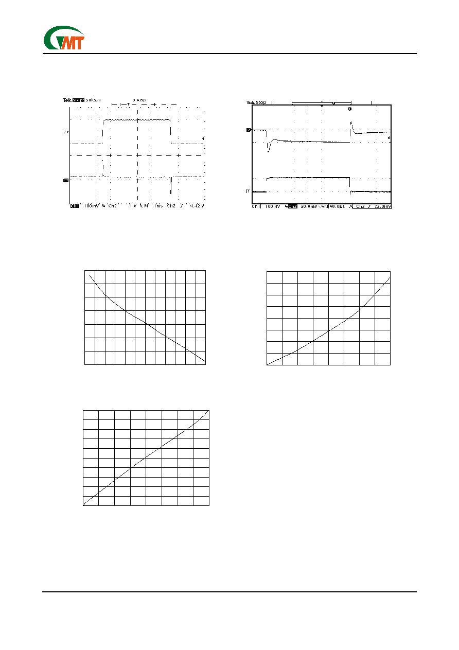
Typical Performance Characteristics
(V
IN
=5V, C
IN
=1µF , C
OUT
=10µF, T
A
=25∞C , unless otherwise noted.)
Ch1: Vout (offset=3.50V)
Ch1: Iout (400mA/div)
Ch2: Vin (offset=5.0V)
Ch2: Vout (offset=3.50V)
Iout=100mA
Ground Current vs. Load Current
Line Transient
Load Transient
Output Voltage vs. Load Current
Dropout Voltage vs. Load Current
3.49
3.50
3.51
3.52
3.53
3.54
3.55
3.56
0
100
200
300
400
500
600
Load Current (mA)
Output Voltage (V)
0
100
200
300
400
500
600
700
800
0
100
200
300
400
Load Current (mA)
Dropout Voltage (mV)
0.60
0.70
0.80
0.90
1.00
1.10
1.20
1.30
1.40
1.50
1.60
0
100
200
300
400
Load Current (mA)
Ground Current (mA)
Ver: 4.5
May 13, 2002
TEL: 886-3-5788833
http://www.gmt.com.tw
4
G930/G931
Global Mixed-mode Technology Inc.
Recommended Minimum Footprint
Note: V
IN(max)
<= 6.5V
0
50
100
150
200
250
300
350
400
450
500
0.0
0.5
1.0
1.5
2.0
2.5
3.0
Input-Output Voltage Differential V
IN
-V
OUT
(V)
Output Current (mA)
TA=25
TA=55
TA=85
Maximum Recommended Output Current
0
0.1
0.2
0.3
0.4
0.5
0.6
25
35
45
55
65
75
85
95
105
115
125
Amibent Temperature T
A
(∞C)
Power Dissipation (W)
T
A
=25∞C,Still Air
Safe Operating Area
[Power Dissipation Limit]
1oz Copper on SOT-89 Package
Mounted on recommended mimimum footprint (RJA=250∞C/W)
Still Air
1oz Copper on SOT89 Package
Mounted on recommend mimimum footprint (RJA=250∞C/W)
Maximum Power Dissipation of SOT-89
Ver: 4.5
May 13, 2002
TEL: 886-3-5788833
http://www.gmt.com.tw
5
G930/G931
Global Mixed-mode Technology Inc.
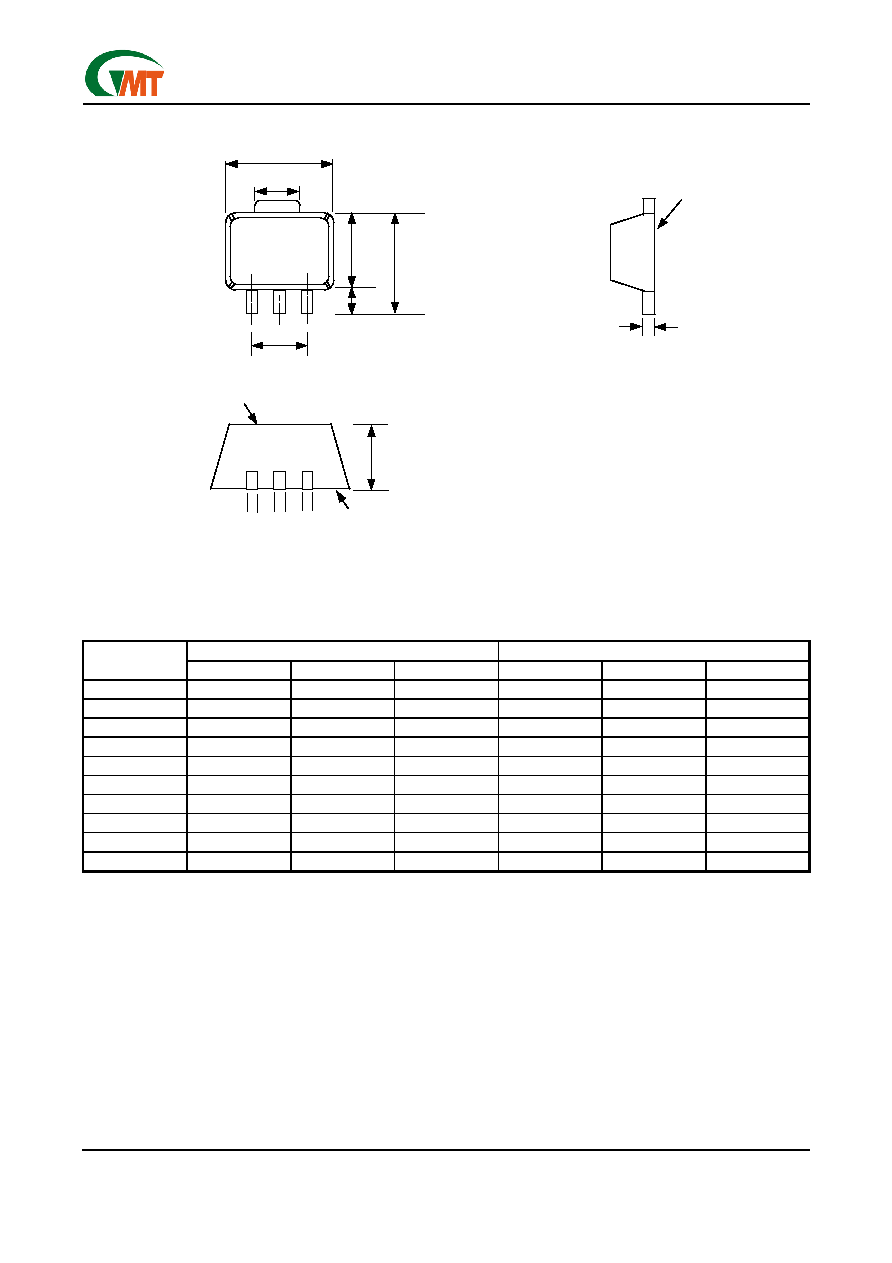
Package Information
SOT- 89 (T2) Package
DIMENSIONS IN MILLIMETERS
DIMENSIONS IN INCHES
SYMBOLS
MIN NOM MAX MIN NOM MAX
A 1.40
1.50
1.60
0.055
0.059
0.063
A1 0.80 1.04 ----- 0.031 0.041 -----
b 0.36
0.42
0.48
0.014
0.016
0.048
b1 0.41 0.47 0.53
0.016
0.018
0.020
C 038
0.40
0.43
0.014
0.015
0.017
D 4.40
4.50
4.60
0.173
0.177
0.181
D1 1.40 1.60 1.75
0.055
0.062
0.069
HE ----- ----- 4.25 ----- ----- 0.167
E 2.40
2.50
2.60
0.094
0.098
0.102
e 2.90
3.00
3.10
0.114
0.118
0.122
D
D1
E
A1
HE
e
b
b
b1
A
POLISH
MATTE FINISH
C
POLISH
Ver: 4.5
May 13, 2002
TEL: 886-3-5788833
http://www.gmt.com.tw
6
G930/G931
Global Mixed-mode Technology Inc.
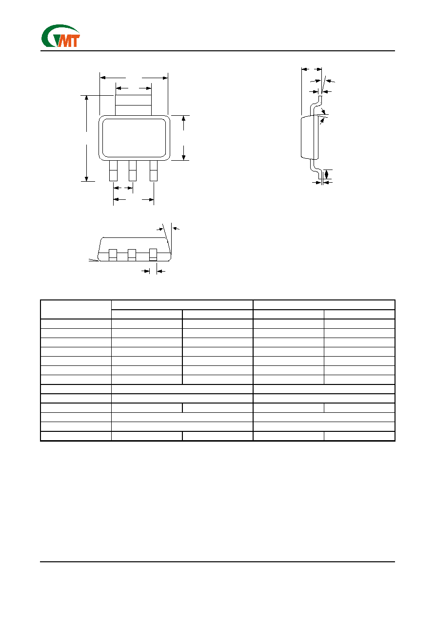
SOT-223 (T6) Package
MILLIMETERS INCHES
SYMBOLS
MIN MAX MIN MAX
A 1.55
1.80
0.061
0.071
A1 0.02 0.12
0.0008
0.0047
B 0.60
0.80
0.024
0.031
B1 2.90 3.10
0.114
0.122
C 0.24
0.32
0.009
0.013
D 6.30
6.70
0.248
0.264
E 3.30
3.70
0.130
0.146
e
2.30 BSC
0.090 BSC
e1
4.60 BSC
0.181 BSC
H 6.70
7.30
0.264
0.287
L
0.90 MIN
0.036 MIN
L2
0.06 BSC
0.0024 BSC
0∫ 10∫ 0∫ 10∫
A
B
13
∞(4X)
A1
e1
e
E
B1
D
H
C
13
∞(4X)
L2
L
Ver: 4.5
May 13, 2002
TEL: 886-3-5788833
http://www.gmt.com.tw
7
G930/G931
Global Mixed-mode Technology Inc.
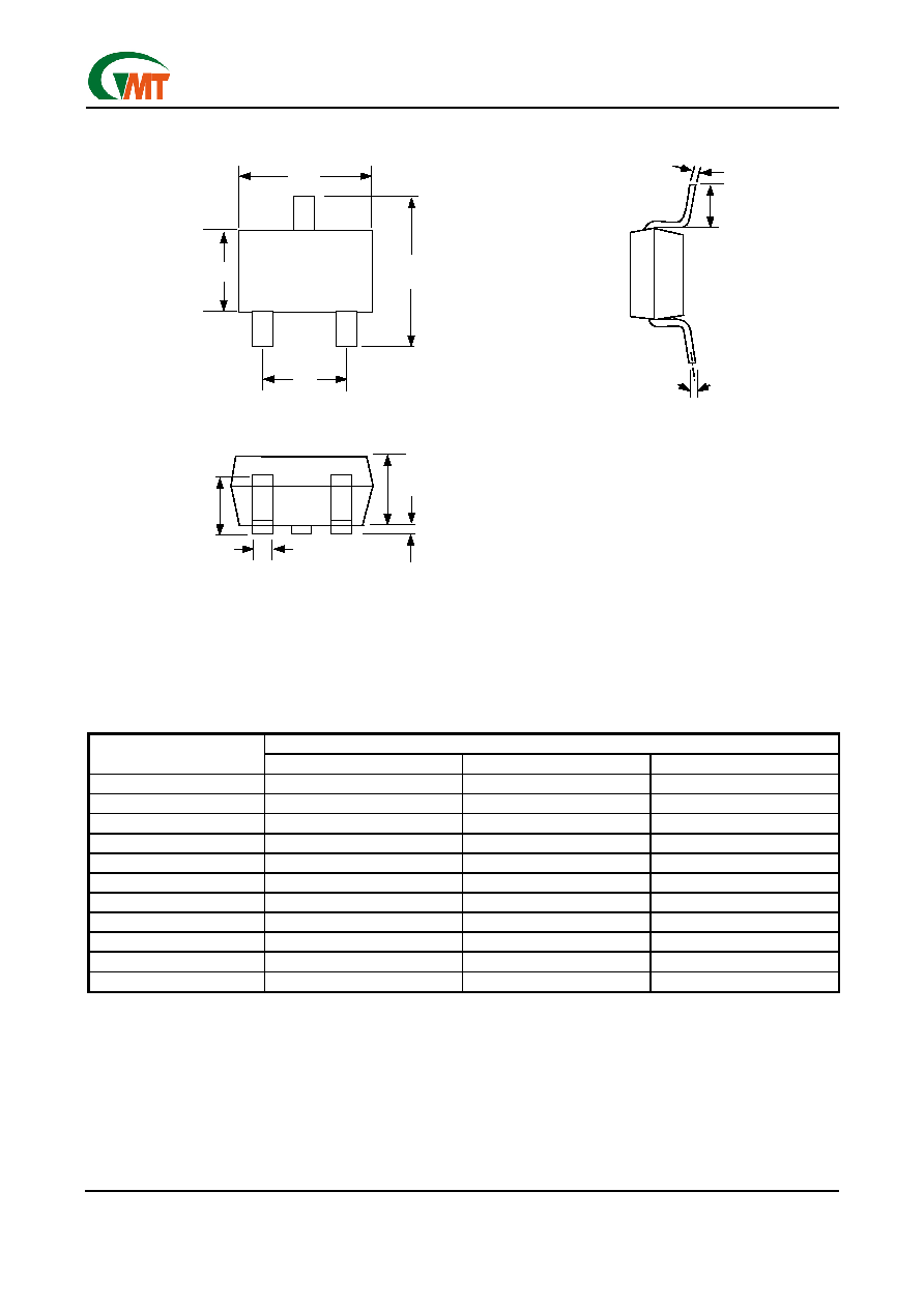
SOT 23 (T7) Package
Note:
1. Package body sizes exclude mold flash protrusions or gate burrs
2. Tolerance ±0.1000 mm (4mil) unless otherwise specified
3. Coplanarity: 0.1000mm
4. Dimension L is measured in gage plane
DIMENSIONS IN MILLIMETERS
SYMBOLS
MIN NOM MAX
A 1.00 1.10 1.30
A1 0.00 ----- 0.10
A2 0.70 0.80 0.90
b 0.35 0.40
0.50
C 0.10 0.15 0.25
D 2.70 2.90 3.10
E 1.40 1.60 1.80
e -----
1.90(TYP)
-----
H 2.60 2.80 3.00
L 0.37 ------ -----
1
1∫ 5∫ 9∫
H
D
e
E
L
C
1
b
A2
A
A1
H
D
e
E
L
C
1
b
A2
A
A1
Ver: 4.5
May 13, 2002
TEL: 886-3-5788833
http://www.gmt.com.tw
8
G930/G931
Global Mixed-mode Technology Inc.
µTO-92 (T8) Package
DIMENSIONS IN MILLIMETERS
DIMENSIONS IN INCHES
SYMBOLS
MIN NOM MAX MIN NOM MAX
A 2.40
2.50
2.60
0.094
0.098
0.102
A1 0.70 0.80 0.90
0.028
0.032
0.036
b 0.35
0.45
0.55
0.014
0.018
0.022
C ----- 0.40 ----- ----- 0.016
-----
D 2.80
3.00
3.20
0.110
0.118
0.126
E 3.80
4.00
4.20
0.149
0.157
0.165
e ----- 1.27 ----- ----- 0.050
-----
F 1.91
2.11
2.31
0.075
0.083
0.091
G 3.35
3.55
3.75
0.132
0.140
0.148
H 0.00 ----- 0.15
0.000
----- 0.006
L 13.80 14.00 14.20 0.543 0.551 0.559
1
----- 2∞ ----- ----- 2∞
-----
2
----- 5∞ ----- ----- 5∞ -----
Package Orientation
GMT Inc. does not assume any responsibility for use of any circuitry described, no circuit patent licenses are implied and GMT Inc. reserves the right at any time without notice to change said circuitry and specifications.
Feed Direction
SOT 23 Package Orientation
Feed Direction
SOT 23 Package Orientation
Feed Direction
SOT 89223 Package Orientation
Feed Direction
SOT 89223 Package Orientation
E
D
L
H
e
b
2 (2 X)
1(2 X)
C
G
A1
A
R2
.0
0
E
D
L
H
e
b
2 (2 X)
1(2 X)
C
G
A1
A
R2
.0
0