 | –≠–ª–µ–∫—Ç—Ä–æ–Ω–Ω—ã–π –∫–æ–º–ø–æ–Ω–µ–Ω—Ç: G960 | –°–∫–∞—á–∞—Ç—å:  PDF PDF  ZIP ZIP |
Ver: 1.4
Jul 31, 2001
TEL: 886-3-5788833
http://www.gmt.com.tw
1
G960
Global Mixed-mode Technology Inc.
3.3V 1A Low Dropout Regulator
Features
Dropout voltage typically 0.8V @ I
O
= 1A
Output current in excess of 1A
Output voltage accuracy ±2%
Quiescent current, typically 600µA
Internal short circuit current limit
Internal over temperature protection
Applications
CD-R/W
ADSL
Cable Modem
Set-Top-Box
LAN switch/Hub
Router
DVD-R/W
General Description
The G960 positive 3.3V voltage regulator features
the ability to source 1A of output current with a
dropout voltage of typically 0.8V over the entire op-
erating temperature range. A low quiescent current
is provided over the entire current output current
range. The typical quiescent current is 0.6mA. Fur-
thermore, the quiescent current is smaller when the
regulator is in the dropout mode (V
IN
< 3.3V).
Familiar regulator features such as over tempera-
ture and over current protection circuits are pro-
vided to prevent it from being damaged by ab-
normal operating conditions.
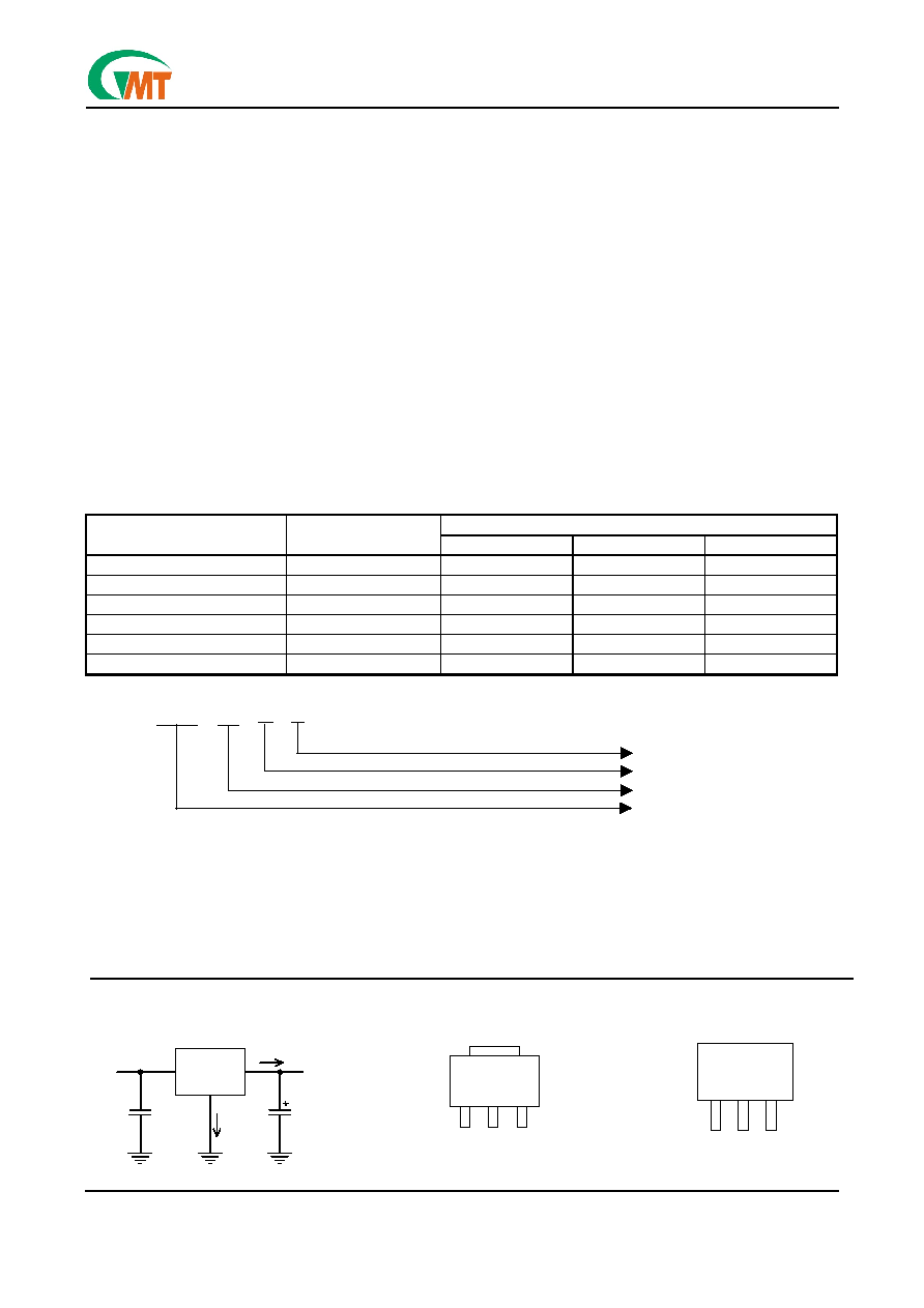
Ordering Information
PIN OPTION
ORDER NUMBER
PACKAGE TYPE
1 2 3
G960T33T TO220
GND
V
OUT
V
IN
G960T36T TO220
V
IN
V
OUT
GND
G960T43U TO252
GND
V
OUT
V
IN
G960T45U TO252
V
IN
GND V
OUT
G960T53U TO263
GND
V
OUT
V
IN
G960T63U SOT223
GND
V
OUT
V
IN
Order Number Identification
GXXX XX X X
Packing Type
Pin Option
Package Type
Part Number
PACKAGE TYPE
PIN OPTION
PACKING
T3 : TO 220
1
2
3
U & D : Tape & Reel Direction
T4 : TO 252
1 : V
OUT
GND V
IN
T : Tube
T5 : TO 263
2 : V
OUT
V
IN
GND
T6 : SOT 223
3 : GND
V
OUT
V
IN
4 : GND
V
IN
V
OUT
5 : V
IN
GND
V
OUT
6 : V
IN
V
OUT
GND
Typical Application Package Type
[Note 4] : Type of C
OUT
G960
C1
0.47µF
IQ
V
IN
V
OUT
I
O
C
OUT
10µF
Top View
1
2
3
SOT 223
Top View
1
2
3
TO 220
252
263

Ver: 1.4
Jul 31, 2001
TEL: 886-3-5788833
http://www.gmt.com.tw
2
G960
Global Mixed-mode Technology Inc.
Absolute Maximum Ratings
(Note 1)
Input Voltage..................................................10V
Power Dissipation Internally Limited (Note
2)
Maximum Junction Temperature..........................150∞C
Storage Temperature Range.........-65∞C
T
J
+150∞C
Lead Temperature, Time for Wave Soldering
TO-220 Package....................................260∞C, 10s
TO-252 Package.....................................260∞C, 4s
SOT-223 Package...................................260∞C, 4s
Operating Conditions
(Note 1)
Input Voltage..............................................4V~7V
Temperature Range.....................-40∞C
T
J
125∞C
Electrical Characteristics
V
IN
=5V, I
O
= 1A, C
IN
= 1µF, C
OUT
=10µF, All specifications apply for T
A
= T
J
= 25∞C. [Note 3]
PARAMETER CONDITIONS MIN
TYP
MAX
UNITS
Output Voltage
50mA < I
O
<400mA
3.234 3.3 3.366 V
Line Regulation
4V < V
IN
< 7V, I
O
= 10mA
20
50
mV
Load Regulation
50mA < I
O
< 1A
30
80
mV
Output Impedance
100mA DC and 20mA AC, fo = 120Hz
100
m
Quiescent Current
V
IN
=
5V
0.6 mA
Ripple Rejection
f
i
= 120Hz, 1V
P-P
,
Io = 100mA
42
dB
I
O
= 1A
0.8
V
Dropout Voltage
I
O
= 100mA
200
mV
Short Circuit Current
1.6
1.9
A
Over Temperature
125
∞C
Note 1: Absolute Maximum Ratings are limits beyond which damage to the device may occur. Operating
Conditions are conditions under which the device functions but the specifications might not be guaranteed. For
guaranteed specifications and test conditions see the Electrical Characteristics.
Note 2: The maximum allowable power dissipation is a function of the maximum junction temperature, T
J
, the junc-
tion-to-ambient thermal resistance, R
JA
, and the ambient temperature, T
A
. Exceeding the maximum allow-
able power dissipation will cause excessive die temperature, and the regulator will go into thermal shut-
down.
Note3: Low duty pulse techniques are used during test to maintain junction temperature as close to ambient as pos-
sible.
Note4: The type of output capacitor should be tantalum or aluminum.
Definitions
Dropout Voltage
The input/output Voltage differential at which the regu-
lator output no longer maintains regulation against
further reductions in input voltage. Measured when the
output drops 100mV below its nominal value, dropout
voltage is affected by junction temperature, load cur-
rent and minimum input supply requirements.
Line Regulation
The change in output voltage for a change in input
voltage. The measurement is made under conditions
of low dissipation or by using pulse techniques such
that average chip temperature is not significantly af-
fected.
Load Regulation
The change in output voltage for a change in load
current at constant chip temperature. The measure-
ment is made under conditions of low dissipation or by
using pulse techniques such that average chip tem-
perature is not significantly affected.
Maximum Power Dissipation
The maximum total device dissipation for which the
regulator will operate within specifications.
Quiescent Bias Current
Current which is used to operate the regulator chip
and is not delivered to the load.
Ver: 1.4
Jul 31, 2001
TEL: 886-3-5788833
http://www.gmt.com.tw
3
G960
Global Mixed-mode Technology Inc.
Typical Performance Characteristics
(V
IN
=5V , C
IN
=1µF , C
OUT
=10µF, T
A
=25∞C , unless otherwise noted.)
Ch1: Vout (offset=3.30V)
Ch1: Vout (offset=3.30V)
Ch2: Vin (offset=5.0V)
Ch2: Iout (780mA/div)
CIN = 2.2µF
Iout=100mA
Ground Current vs. Load Current
Line Transient
Load Transient
Output Voltage vs. Load Current
Dropout Voltage vs. Load Current
0
100
200
300
400
500
600
700
800
0
200
400
600
800
1000
Load Current (mA)
Dropout Voltage (mV)
3.293
3.298
3.303
3.308
3.313
3.318
3.323
0
200
400
600
800
1000
Load Current (mA)
Output Voltage (V)
0.6
0.8
1.0
1.2
1.4
1.6
1.8
0
100
200
300
400
500
600
700
800
900
1000
Load Current (mA)
Ground Current (mA)

Ver: 1.4
Jul 31, 2001
TEL: 886-3-5788833
http://www.gmt.com.tw
4
G960
Global Mixed-mode Technology Inc.
Package Information
TO-220 (T3) Package
MILLIMETERS INCHES
SYMBOLS
MIN MAX MIN MAX
A 4.318 4.826 0.170 0.190
A1 2.46 2.72
0.097
0.107
b 0.69
0.94
0.027
0.037
b1 1.143 1.397 0.045 0.055
C 0.304 0.460 0.012 0.018
D 3.429 3.683 0.135 0.145
D1 8.53 9.04
0.336
0.356
d 2.62
2.87
0.103
0.113
E 9.906 10.40 0.390 0.410
E1 2.84 5.13
0.112
0.202
e 2.29
2.79
0.090
0.110
e1 4.83 5.33
0.190
0.210
F 1.143 1.397 0.045 0.055
I 3.454 3.962 0.136 0.156
L 13.589
14.351
0.535
0.565
E
R
E1
E1
D
d
I
L
e
b
b1
e1
A
F
D1
C
A1

Ver: 1.4
Jul 31, 2001
TEL: 886-3-5788833
http://www.gmt.com.tw
5
G960
Global Mixed-mode Technology Inc.
TO-252 (T4) Package
Notes:
1. Dimensioning and tolerancing per ansi y14.5m, 1982.
2. Controlling dimension: inch
MILLIMETERS INCHES
SYMBOLS
MIN MIN MAX MAX
A 5.97
0.235
0.250
6.35
B 6.35
0.250
0.265
6.73
C 2.19
0.086
0.094
2.38
D 0.69
0.027
0.035
0.88
E 0.84
0.033
0.040
1.01
F 0.94
0.037
0.047
1.19
G 4.58BSC
0.180BSC
H 0.87
0.034
0.040
1.01
J 0.46
0.018
0.023
0.58
K 2.60
0.102
0.114
2.89
L 2.29BSC
0.090BSC
R 4.45
0.175
0.215
6.46
S 0.51
0.020
0.050
1.27
U 0.51
0.020 --- ---
V 0.77
0.030
0.050
1.27
Z 3.51
0.138 --- ---
R
B
V
A
K
S
1
2
3
F
L
D
G
4
2 PL
0.13 (0.005) M T
Z
E
C
T
SEATING
PLANE
U
J
H

Ver: 1.4
Jul 31, 2001
TEL: 886-3-5788833
http://www.gmt.com.tw
6
G960
Global Mixed-mode Technology Inc.
TO-263 (T5) Package
MILLIMETERS INCHES
SYMBOLS
MIN MAX MIN MAX
A 4.30
4.70
0.169
0.185
A1 1.22 1.32
0.048
0.055
A2 2.45 2.69
0.104
0.106
b 0.69
0.94
0.027
0.037
b1 1.22 1.40
0.048
0.055
C 0.36
0.56
0.014
0.022
D 8.64
9.652
0.340
0.380
E 9.70
10.54
0.382
0.415
e 2.29
2.79
0.090
0.110
e1 4.83 5.33
0.190
0.210
H 14.60 15.78 0.575 0.625
L 4.70
5.84
0.185
0.230
L1 1.20
1.778
0.047
0.070
L2 2.24 2.84
0.088
0.111
L3 1.40MAX
0.055MAX
e
L3
D
H
e1
b1
b
E
A
A1
C
A2
L2
L
L1

Ver: 1.4
Jul 31, 2001
TEL: 886-3-5788833
http://www.gmt.com.tw
7
G960
Global Mixed-mode Technology Inc.
SOT-223 (T6) Package
MILLIMETERS INCHES
SYMBOLS
MIN MAX MIN MAX
A 1.55
1.80
0.061
0.071
A1 0.02 0.12
0.0008
0.0047
B 0.60
0.80
0.024
0.031
B1 2.90 3.10
0.114
0.122
C 0.24
0.32
0.009
0.013
D 6.30
6.70
0.248
0.264
E 3.30
3.70
0.130
0.146
e
2.30 BSC
0.090 BSC
e1
4.60 BSC
0.181 BSC
H 6.70
7.30
0.264
0.287
L
0.90 MIN
0.036 MIN
L2
0.06 BSC
0.0024 BSC
0∫ 10∫ 0∫ 10∫
Package Orientation
A
B
13
∞
(4X)
A1
e1
e
E
B1
D
H
C
13
∞
(4X)
L2
L
Feed Direction
SOT 223 Package Orientation
Feed Direction
SOT 223 Package Orientation
Feed Direction
TO 220
252
263 Package Orientation
Feed Direction
TO 220
252
263 Package Orientation