 | –≠–ª–µ–∫—Ç—Ä–æ–Ω–Ω—ã–π –∫–æ–º–ø–æ–Ω–µ–Ω—Ç: G9611AP1U | –°–∫–∞—á–∞—Ç—å:  PDF PDF  ZIP ZIP |
Ver: 1.4
Jun 29, 2004
TEL: 886-3-5788833
http://www.gmt.com.tw
1
G9611
Global Mixed-mode Technology Inc.
Low-Dropout, 300mA Linear Regulator with Reset
Features
300mA Output Current, with Foldback Current
Limiting
High Ripple Rejection
±2% Output Accuracy
±2% Reset Threshold Accuracy
Externally Programmable Reset Time Delay
Generator
Internal 300mA P-Channel Pass Transistor
320µA quiescent Current
Thermal Overload Protection
SOP 8 Package
Applications
CD ROM or DVD ROM
Slim-Type CD/DVD
DVD Player
General Description
The G9611 are low-dropout, linear regulator with
reset function supply 3.4V, 3.3V or 2.5V output for
currents up to 300mA. They are available in a
700mW SOP 8 package. Typical dropouts are
320mV at 300mA. Shutdown turns off linear regu-
lator function. Other features include foldback cur-
rent limiting and thermal overload protection.
The reset function in G9611 detect V
CC
level with
hysteresis, keeping it asserted for time delay de-
termined by external capacitor. The reset output is
active low open-drain output. The detection thresh-
old are 3.9V or 4.2V.
The output is preset at 3.4V for the G9611A, 3.3V
for the G9611B/C, and 2.5V for G9611D. The reset
threshold is preset at 4.2V for G9611 A/B/D and
3.9V for G9611C.
Ordering Information
PART
NUMBER
MARKING
REGULATOR
OUTPUT VOLTAGE
RESET THRESHOLD
VOLTAGE
TEMP.
RANGE
PIN-
PACKAGE
G9611AP1x
G9611A
3.4
4.2
-40∞C to +85∞C
SOP-8L
G9611BP1x
G9611B
3.3
4.2
-40∞C to +85∞C
SOP-8L
G9611CP1x
G9611C
3.3
3.9
-40∞C to +85∞C
SOP-8L
G9611DP1x
G9611D
2.5
4.2
-40∞C to +85∞C
SOP-8L
Note: X Specify the packing type
U: Tape & Reel T: Tube
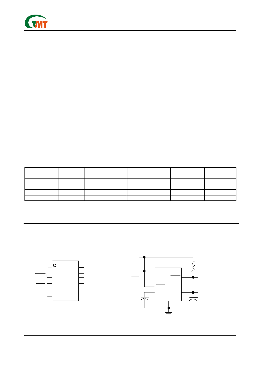
Pin configuration
Typical Operation Circuit
8
6
5
1
2
3
4
N.C
RESET
V
IN
C
D
GND
N.C
V
OUT
SOP- 8L
G9611
7
V
IN
RESET
C
D
GND
SHDN
G9611
OUTPUT
VOLTAGE
V
OUT
10µF
(Tantalum or Aluminum)
10k
V
CC
SHDN
R
pull-high
1µF
8
6
5
1
2
3
4
N.C
RESET
V
IN
C
D
GND
N.C
V
OUT
SOP- 8L
G9611
7
V
IN
RESET
C
D
GND
SHDN
G9611
OUTPUT
VOLTAGE
V
OUT
10µF
(Tantalum or Aluminum)
10k
V
CC
SHDN
R
pull-high
1µF
Ver: 1.4
Jun 29, 2004
TEL: 886-3-5788833
http://www.gmt.com.tw
2
G9611
Global Mixed-mode Technology Inc.
Absolute Maximum Ratings
Supply Voltage (IN or OUT to GND........-0.3V to +6.5V
Output Short-Circuit Duration............................1 min
Input Voltage ..........................-0.3V to the greater of
(IN+0.3V) or (OUT + 0.3V)
Continuous Power Dissipation (T
A
= +25∞C)......700mW
Operating Temperature Range............ -40∞C to +85∞C
Junction Temperature..................................+160∞C
Storage Temperature Range..............-65∞C to +160∞C
Lead Temperature (soldering, 10sec)...............+260∞C
Stresses beyond those listed under "Absolute Maximum Ratings" may cause permanent damage to the device. These are stress ratings
only, and functional operation of the device at these or any other conditions beyond those indicated in the operational sections of the
specifications is not implied. Exposure to absolute maximum rating conditions for extended periods may affect device reliability
Electrical Characteristics
V
IN
=5V, C
IN
=1µF, C
OUT
=10µF,
SHDN =V
IN
, T
J
=T
A
=25∞C (Note3), unless otherwise noted. Typical values for
regulators are at V
IN
=5V.
PARAMETER SYMBOL CONDITION MIN
TYP
MAX
UNIT
Input Voltage
V
IN
2.5 --- 6.0
V
G9611A 3.332
3.4
3.468
G9611B/C 3.234
3.3
3.366
Output Voltage (Note 1)
V
OUT
G9611D 2.45
2.5
2.55
V
Load Regulation
V
LDR
I
OUT
=1mA to 300mA, V
IN
=V
OUT
+1V --- 6 15 mV
Line Regulation
V
LNR
(V
OUT
+0.5V)
V
IN
6V, I
OUT
=25mA
-8 0.3 8 mV
Dropout Voltage (Note 2)
V
DO
I
OUT
=300mA ---
320
400
mV
Parameter Tempco V
OUT
---
40
---
ppm/∞C
f=120HZ, I
OUT
=30mA ---
70
---
Ripple Rejection
PSRR
f=120HZ, I
OUT
=300mA ---
65
---
dB
Output Noise
e
n
20Hz to 100kHz, I
OUT
=30mA. ---
350
---
µ
V
RMS
Quiescent Current
I
Q
--- 320 450 µA
OFF Quiescent Current
I
QOFF
SHDN
0.4V
--- 140 200 µA
V
OUT
<V
FOLDBACK
260
400
580
Foldback Current Limit
I
LIM
V
OUT
>V
FOLDBACK
650
900
1200
mA
Foldback Voltage
V
FOLDBACK
0.6
0.78
0.95
V
Thermal Shutdown Temperature
T
SD
--- 160 ---
∞C
Thermal Shutdown Hysteresis
T
SD
---
30
---
∞C
SHDN Pin Input High Threshold
V
IH_
SHDN
1.8
2
2.3
V
SHDN Pin Input Low Threshold
V
IL_
SHDN
0.6
0.8
1.1
V
G9611A/B/D 4.11
4.2
4.29
Reset Threshold
V
TH-
G9611C 3.81
3.9
3.99
V
G9611A/B/D ---
150
---
Reset Threshold Hysteresis
V
HYS
G9611C ---
130
---
mV
Reset Threshold Tempco
---
40
---
ppm/∞C
C
D
Delay Pin Threshold Voltage
V
TCD
V
CC
= 5V
3.5
3.9
4.3
V
C
D
Pin Sink Current
I
CD
V
CC
=1.5V, V
CD
=0.5V 3
4.3
---
mA
C
D
Pin Pullup Resistance
R
D
100 200 400 k
RESET Output Current Low
I
OL
V
CC
=2.5V, V
RESET
=0.4V
8 11.5 --- mA
RESET Function Operating Voltage
V
OP
RESET
sink current>10µA
--- 0.7 0.85 V
Note 1: (V
IN
-V
OUT
) is limited to keep the product (I
OUT
x (V
IN
- V
OUT
)) from exceeding the package power dissipation
limits.
Note 2: Dropout Voltage is (V
IN
- V
OUT
) when V
OUT
falls to 100mV below its nominal value at V
IN
= V
OUT
+1V. For
example, the G9611 is tested by measuring the V
OUT
at V
IN
= V
OUT
+1V, then V
IN
is lowered until V
OUT
falls
100mV below the measured value. The difference (V
IN
- V
OUT
) is then measured and defined as
V
DO
.
Note 3: Low duty pulse techniques are used during test to maintain junction temperature as close to ambient as possible.

Ver: 1.4
Jun 29, 2004
TEL: 886-3-5788833
http://www.gmt.com.tw
3
G9611
Global Mixed-mode Technology Inc.
Typical Performance Characteristics
(V
IN
=5V,C
IN
=C
OUT
=10µF, SHDN =V
IN
, T
J
=25∞C, unless otherwise noted)
SHDN Pin vs. Output
Load transient
Line Transient
Line Transient
Over Current Response
Short Circuit Response
Ver: 1.4
Jun 29, 2004
TEL: 886-3-5788833
http://www.gmt.com.tw
4
G9611
Global Mixed-mode Technology Inc.
Typical Performance Characteristics
(continued)
0.255
0.26
0.265
0.27
0.275
0.28
0.285
0.29
0.295
0.3
0.305
0.5 0.7 0.9 1.1 1.3 1.5 1.7 1.9 2.1 2.3 2.5 2.7
Input -Output Voltage Differential(V)
Load Current (A)
Power Supply Rejection Ratio
Power Supply Rejection Ratio
Power Supply Rejection Ratio
Safe Operating Area of G9611 SO-8
T
A
=25∞C

Ver: 1.4
Jun 29, 2004
TEL: 886-3-5788833
http://www.gmt.com.tw
5
G9611
Global Mixed-mode Technology Inc.
Pin Description
PIN NO.
PIN NAME
PIN FUNCTION
1, 6
N.C
No Connection.
2
RESET
RESET
Open-Drain Output remains low while V
IN
is below the reset threshold,
and for delay time set by C
D
after V
IN
rises above the reset threshold.
3
SHDN
SHDN
= High to enable regulator output.
SHDN
= Low to shutdown regulator output.
4 V
IN
Regulator Input. Supply voltage can range from 2.5V to 6V.
5 V
OUT
Regulator Output. Sources up to 300mA.
7 GND
Ground
8 C
D
External Programmable time delay is set by the capacitor connect to C
D
pin.
Figure 1. Functional Diagram
Detailed Description
The G9611 are low-dropout, low-quiescent current
linear regulators with reset function The regulator in
G9611 supply 3.4V, 3.3V or 2.5V output for load cur-
rents up to 300mA. The reset function detect V
IN.
As
illustrated in Figure 1, they consist of a 1.24V refer-
ence, error amplifier, MOSFET driver, P-channel pass
transistor, and internal feedback voltage divider, reset
threshold comparator and time delay generator.
The 1.24V bandgap reference is connected to the er-
ror amplifier's inverting input. The error amplifier com-
pares this reference with the feedback voltage and
amplifies the difference. The MOSFET driver reads the
error signal and applies the appropriate drive to the
P-channel pass transistor. If the feedback voltage is
lower than the reference, the pass transistor gate is
pulled lower, allowing more current to pass and in-
creasing the output voltage. If the feedback voltage is
too high, the pass transistor gate is pulled up, allowing
less current to pass to the output.
Additional blocks of linear regulator include a foldback
current limiter, thermal sensor, and shutdown logic.
The G9611 also offer reset function to detect the level
of V
IN
. They assert a reset signal whenever V
IN
supply
voltage declines below a preset threshold (V
TH
), keep-
ing it asserted for time delay set by capacitor con-
nected to C
D
pin, after V
IN
has resen above the high
reset threshold (V
TH
+ V
HYS
). The
RESET
is an active
low, open-drain output.
Internal P-Channel Pass Transistor
The G9611 feature a 300mA P-channel MOSFET
pass transistor. This provides several advantages over
similar designs using PNP pass transistors, including
longer battery life. The P-channel MOSFET requires
no base drive, which reduces quiescent current con-
siderably. PNP based regulators waste considerable
amounts of current in dropout when the pass transistor
saturates. They also use high base-drive currents un-
der large loads. The G9611 do not suffer from these
problems and consume only 320µA of quiescent cur-
rent.
V
OUT
SHUTDOWN
LOGIC
1.24V
REFERENCE
MOSFET DRIVER
WITH FOLDBACK
CURRENT LIMIT
R1
R2
THERMAL
PROTECTION
P
SHDN
C
D
R
D
V
IN
GND
RESET
V
OUT
SHUTDOWN
LOGIC
1.24V
REFERENCE
MOSFET DRIVER
WITH FOLDBACK
CURRENT LIMIT
R1
R2
THERMAL
PROTECTION
P
SHDN
C
D
R
D
V
IN
GND
RESET