Ver: 0.8 Preliminary
Apr 01, 2005
TEL: 886-3-5788833
http://www.gmt.com.tw
1
G962
Global Mixed-mode Technology Inc.
2A Low Dropout Regulator with Enable
Features
Adjustable Output from 1.2V to 4.8V Using Ex-
ternal Resistors
1.5V, 1.8V and 2.5V options by Setting ADJ Pin
Below 0.2V
Over current and over temperature protection
500mV dropout @2A
Enable pin
10µA quiescent current in shutdown
Output recovery mode in OTP
Connect ADJ to GND for fixed output mode
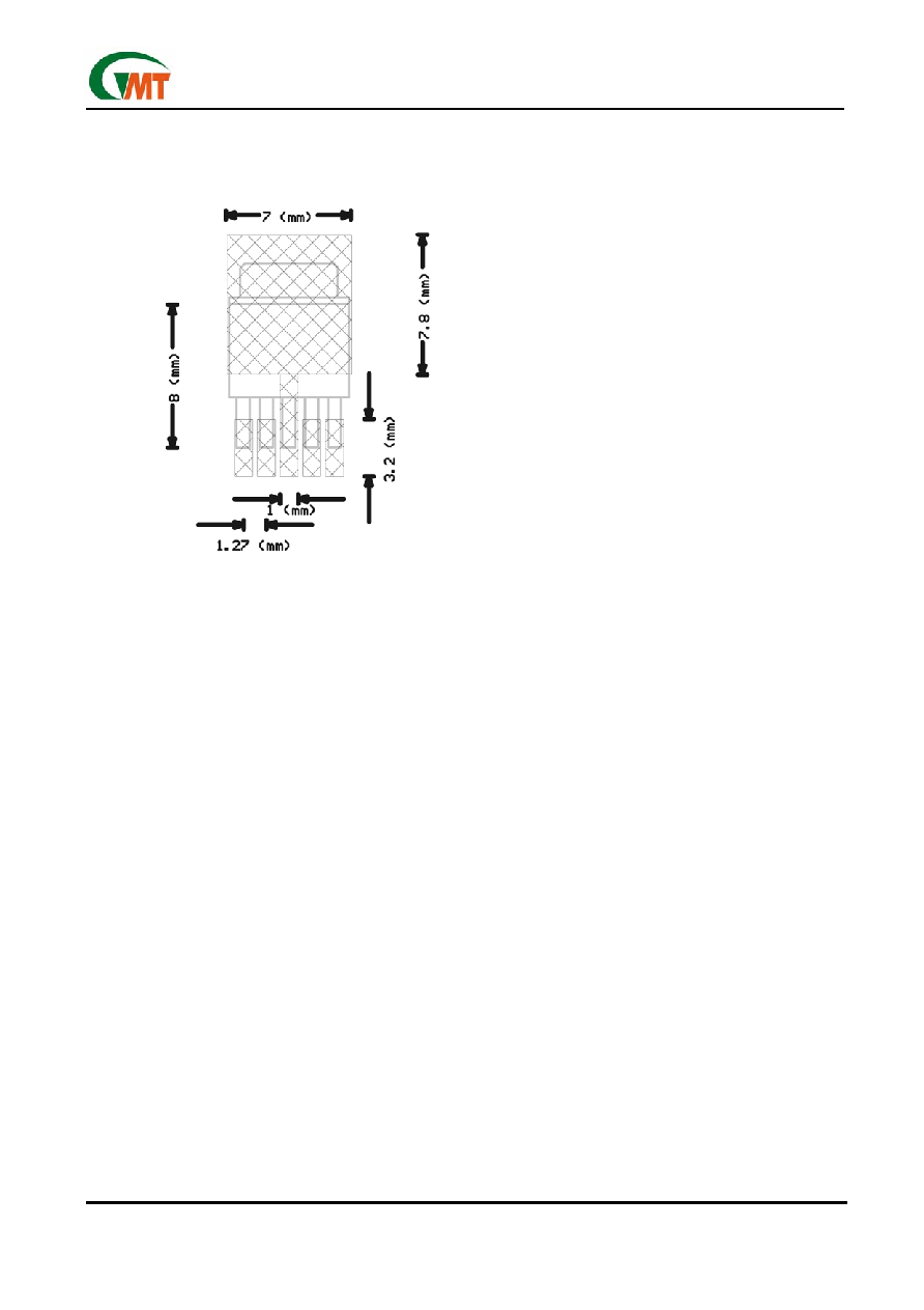
TO-252-5 Package
Applications
Battery powered systems
Motherboards
Peripheral cards
Set Top Boxes
Notebook Computers
General Description
The G962 is a high performance positive voltage
regulator designed for use in applications requiring
very low dropout voltage at up to 2 Amps. Since it has
superior dropout characteristics compared to regular
LDOs, it can be used to supply 2.5V on motherboards
or 1.5V, 1.8V on peripheral cards from the 3.3V supply
thus allowing the elimination of costly heatsinks. An
enable pin further reduces power dissipation while
shut down. The G962 provides excellent regulation
over variations in line, load and temperature.
The TO-252-5 is available with 1.5V, 1.8V and 2.5V
internally preset outputs that are also adjustable using
external resistors.
Ordering Information
ORDER NUMBER
ORDER NUMBER
(Pb free)
MARKING TEMP.
RANGE PACKAGE
G962-15ADJTJU G962-15ADJTJUf
G962-15
-40∞C ~ +85∞C
TO-252-5
G962-18ADJTJU G962-18ADJTJUf
G962-18
-40∞C ~ +85∞C
TO-252-5
G962-25ADJTJU G962-25ADJTJUf
G962-25
-40∞C ~ +85∞C
TO-252-5
Note:
TJ:TO-252-5
U : Tape & Reel
e.g. 18 denotes the 1.8V output voltage.
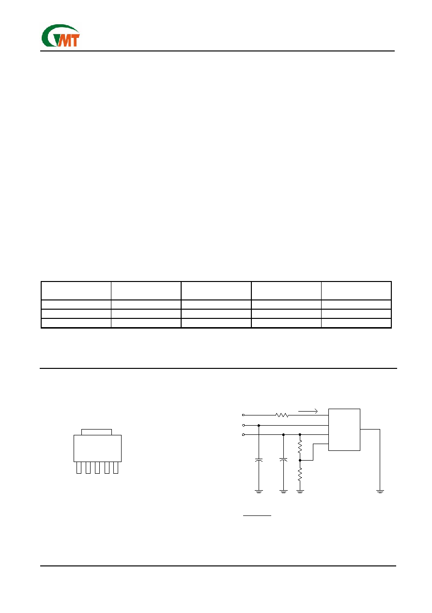
Pin Configuration Typical Application Circuit
VEN
VIN
VO
C1
47µF
C2
100µF
R1
R2
VEN
VIN
VO
ADJ
GND
G962
1.2 (R1+R2)
VO =
R2
Volts
TO-252-5
Top View
1
3
2
4
5
EN VIN GND VO ADJ
R2=12k
is recommended
R3
I
ENH
R3 should be connected for current I
ENH
restriction as V
EN
> V
IN
+0.3V
VEN
VIN
VO
C1
47µF
C2
100µF
R1
R2
VEN
VIN
VO
ADJ
GND
G962
1.2 (R1+R2)
VO =
R2
Volts
TO-252-5
Top View
1
3
2
4
5
EN VIN GND VO ADJ
R2=12k
is recommended
R3
I
ENH
R3 should be connected for current I
ENH
restriction as V
EN
> V
IN
+0.3V

Ver: 0.8 Preliminary
Apr 01, 2005
TEL: 886-3-5788833
http://www.gmt.com.tw
2
G962
Global Mixed-mode Technology Inc.
Absolute Maximum Ratings
(Note 1)
Input Voltage....................................................7V
V
EN
Voltage..............................................V
IN
+0.3V
Power Dissipation Internally Limited (Note 2)
Maximum Junction Temperature.......................150∞C
Storage Temperature Range.........-65∞C
T
J
+150∞C
Reflow Temperature (Soldering, 10 sec)...........260∞C
Thermal Resistance Junction to Ambient, (
JA
)
TO-252-5................................................95∞C/W
Thermal Resistance Junction to Case, (
JC
)
TO-252-5.......................................................8∞C/W
ESD Rating (Human Body Model)......................2kV
Operation Conditions
(Note 1)
Input Voltage..........................................2.2V ~7V
Temperature Range.....................-40∞C
T
A
+85∞C
Electrical Characteristics
V
EN
=V
IN
, V
IN
=5V, I
O
= 0.5A, C
IN
= 4.7µF, C
OUT
=10µF, T
A
= T
J
= 25∞C unless otherwise specified (Note 3)
PARAMETER SYMBOL
CONDITION
MIN
TYP
MAX
UNIT
Output Voltage
V
O
V
IN
=V
O
+0.7V, I
O
=10mA -2
V
O
2 %
Line Regulation
V
O
+0.7V < V
IN
< 5.5V, I
O
=10mA ---
0.2
2
%
Load Regulation
10mA < I
O
< 2A
---
0.8
2
%
V
IN
=3.3V,V
EN
=V
IN
---
1.7
2.5
mA
Quiescent Current
I
Q
V
IN
=3.3V,V
EN
=0V
---
16
35
µA
Ripple Rejection
fi=120Hz, 1V
P-P
, I
O
=100mA ---
55
---
dB
Dropout Voltage
V
D
I
O
=2A ---
0.7
0.85
V
Short Circuit Current
---
0.8
---
A
Over Temperature
(Note 4)
---
150
---
∞C
V
EN
Voltage High
V
ENH
Output
Active
1.6 --- ---
V
V
EN
Voltage Low
V
ENL
Output
Disabled
--- --- 0.4 V
V
EN
Bias Current Low
I
ENL
V
EN
=0.4V ---
---
20
µA
ADJ Reference Voltage
V
REF
V
IN
=2.2V, V
ADJ
=V
OUT
, I
O
=10mA
1.176 1.2 1.224
V
ADJ Pin Threshold
---
0.2
---
V
Note 1:
Absolute Maximum Ratings are limits beyond which damage to the device may occur. Operating Con-
ditions are conditions under which the device functions but the specifications might not be guaranteed. For
guaranteed specifications and test conditions see the Electrical Characteristics.
Note 2:
The maximum power dissipation is a function of the maximum junction temperature, T
Jmax
; total thermal
resistance,
JA
, and ambient temperature T
A
. The maximum allowable power dissipation at any ambient
temperature is (T
jmax
-T
A
)
/
JA
. If this dissipation is exceeded, the die temperature will rise above 150∞C
and IC will go into thermal shutdown.
Note3:
Low duty pulse techniques are used during test to maintain junction temperature as close to ambient as possible.
Note4:
The over temperature point is guarantee by design.
Definitions
Dropout Voltage
The input/output voltage differential at which the regula-
tor output no longer maintains regulation against further
reductions in input voltage. Measured when the output
drops 2% below its nominal value, dropout voltage is
affected by junction temperature, load current and mini-
mum input supply requirements.
Line Regulation
The change in output voltage for a change in input volt-
age. The measurement is made under conditions of low
dissipation or by using pulse techniques such that aver-
age chip temperature is not significantly affected.
Load Regulation
The change in output voltage for a change in load
current at constant chip temperature. The measure-
ment is made under conditions of low dissipation or by
using pulse techniques such that average chip tem-
perature is not significantly affected.
Maximum Power Dissipation
The maximum total device dissipation for which the
regulator will operate within specifications.
Quiescent Bias Current
Current which is used to operate the regulator chip
and is not delivered to the load.
Output Capacitor for Stable Condition
The G962 can be stable for X5R MLCC capacitor lar-
ger than 10µF or POSCAP capacitor larger than 47µF.

Ver: 0.8 Preliminary
Apr 01, 2005
TEL: 886-3-5788833
http://www.gmt.com.tw
4
G962
Global Mixed-mode Technology Inc.
Typical Characteristics
(continued)
1.50
1.55
1.60
1.65
1.70
1.75
1.80
1.85
1.90
1.95
2.00
-25 -15 -5
5 15 25 35 45 55 65 75 85
Temperature (∞C)
Q
u
iesce
nt C
u
rr
en
t (
m
A)
V
IN
=3.0V
V
IN
=5.0V
1.764
1.784
1.804
1.824
1.844
1.864
-25 -15 -5
5 15 25 35 45 55 65 75 85
Temperature (∞C)
O
u
t
p
ut
V
o
lt
age
(
V
)
V
IN
=3.0V
V
IN
=5.0V
1.764
1.784
1.804
1.824
1.844
1.864
2.5
3
3.5
4
4.5
5
5.5
6
6.5
7
V
IN
(V)
O
u
t
put
Vo
l
t
age (
V
)
I
L
=10mA
I
L
=10mA
T=25∞C
T=-25∞C
T=85∞C
0
100
200
300
400
500
600
700
800
900
0
0.5
1
1.5
2
I
L
(A)
D
r
o
pout
V
o
l
t
a
ge
(m
V
)
T=
-
25∞C
T=
8
5∞C
T=25∞C
Max. Power Dissipation vs. T
AMB
(still air)
( Different PCB Top Copper Area )
Quiescent Current vs. Temperature
Dropout Voltage vs. Temperature
Output Voltage vs. Temperature
Output Voltage vs. V
IN
0.0
0.5
1.0
1.5
2.0
2.5
3.0
3.5
4.0
0.5 1.0 1.5 2.0 2.5 3.0 3.5 4.0 4.5 5.0
PCB Top Copper Area (in
2
)
M
a
x
.
Dis
s
i
pation
P
o
wer (W
)
T
AMB
= 25∞C ; Still Air
Max. Power Dissipation vs.
PCB Top Copper Area
0
0.5
1
1.5
2
2.5
3
3.5
4
25
35
45
55
65
75
85
T
AMB
(∞C)
M
a
x
.
Di
s
s
i
pat
i
on
P
o
w
e
r
(W
)
A=0.5
A=1.0
A=1.5
A=2.0
A=2.5
A=3.0
A=3.5
A=4.0
A=4.5
A=5.0
Unit: in
2