Symbols
KBL005 KBL01
KBL02
KBL04
KBL06
KBL08
KBL10
Units
Maximum repetitive peak reverse voltage
V
RRM
50
100
200
400
600
800
1000
Volts
Maximum RMS bridge input voltage
V
RMS
35
70
140
280
420
560
700
Volts
Maximum DC blocking voltage
V
DC
50
100
200
400
600
800
1000
Volts
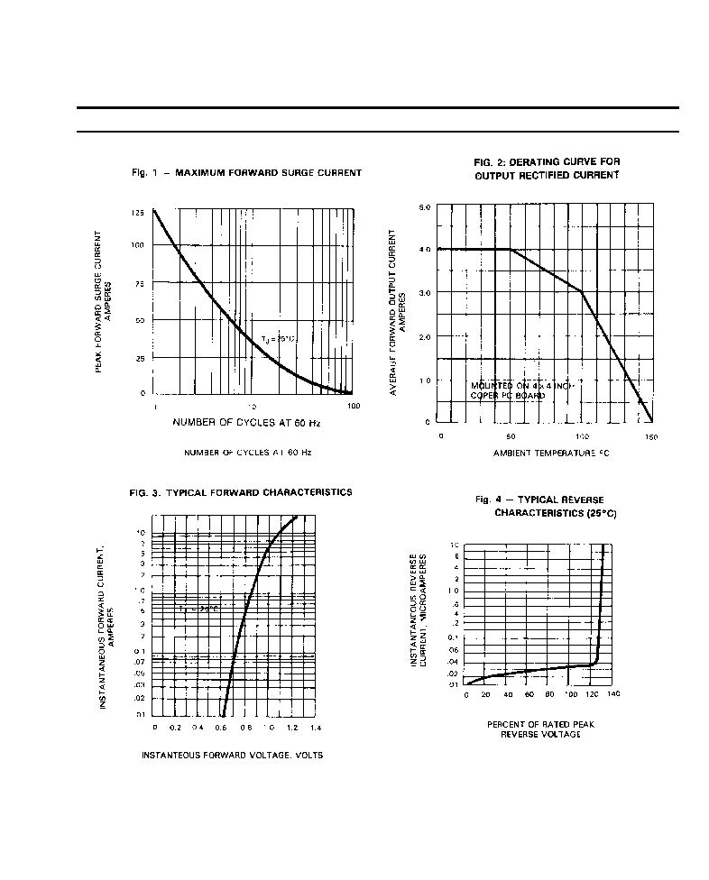
Maximum average forward output current
at T
A
=50 (Note 1)
I
(AV)
4.0
Amps
Peak forward surge current, 8.3mS single
half sine-wave superimposed on rated load
I
FSM
150.0
Amps
Maximum forward Voltage drop per bridge element
at 3.0A peak
V
F
1.0
Volt
Maximum DC reverse current
at rate DC blocking voltage
I
R
10.0
A
Maximum DC reverse current at rated
DC blocking voltage and T
A
=150
I
R
1.0
mA
Operating and storage temperature range
T
J
, T
STG
-55 to +150
Features
KBL005 THRU KBL10
SINGLE-PHASE SILICON BRIDGE
Reverse Voltage -
50 to 1000 Volts
Forward Current -
4.0 Amperes
Ideal for printed circuit board
Surge overload rating - 150 amperes peak
Mounting Position: Any
Lead: Silver-plated copper
Plastic material has Underwriters Laboratory
Flammability Classification 94V-0
Maximum Ratings and Electrical Characteristics
Ratings at 25 ambient temperature unless otherwise specified.
Single phase, half wave, 60Hz, resistive or inductive load.
For capacitive load, derate current by 20%.
Note:
(1) Mounting conditions, 0.5 lead length maximum
1
D IM E N S IO N S
D IM
in c h e s
m m
N o te
M in .
M a x .
M in .
M a x .
A
0 .6 0 5
0 .8 2 5
1 5 .3 6 7
1 6 .3 8 3
B
0 .7 5 0
-
1 9
-
C
0 .7 3 0
0 .7 7 0
1 8 .5 4 2
1 9 .5 5 8
D
0 .2 3 5
0 .2 6 5
5 .9 7
6 .7 3
E
0 .0 7 0 T y p .
1 .7 7 8 T y p .
F
0 .1 9 0
0 .2 1 0
4 .8 3
5 .3 3
G
0 .0 4 8
0 .0 5 2
1 .2 2
1 .3 2
H
0 .1 5 6 x 4 5
o
J
0 .2 0 0 T y p .
5 .0 8 T y p .