Symbols
W005
W01
W02
W04
W06
W08
W10
Units
Maximum repetitive peak reverse voltage
V
RRM
50
100
200
400
600
800
1000
Volts
Maximum RMS voltage
V
RMS
35
70
140
280
420
560
700
Volts
Maximum DC blocking voltage
V
DC
50
100
200
400
600
800
1000
Volts
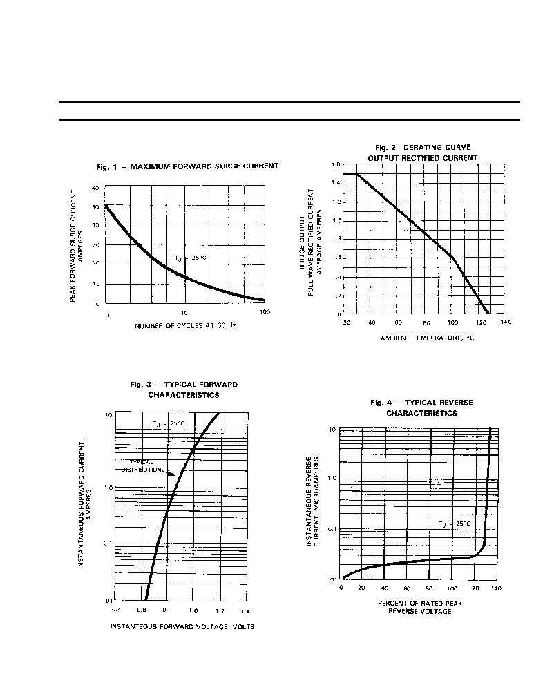
Maximum average forward rectified current
T
A
=25
I
(AV)
1.5
Amps
Peak forward surge current, 8.3mS single
half sine-wave superimposed on rated load
I
FSM
50.0
Amps
1
2
t Rating for fusing (t<8.35ms)
I
2
t
5.0
A
2
t
Maximum forward voltage drop
per element at 1.0A peak
V
F
1.0
Volt
Maximum DC reverse current at rated T
A
=25
DC blocking voltage per element T
A
=100
I
R
10.0
1.0
A
mA
Operating temperature range
T
J
-55 to +125
Storage temperature range
T
STG
-55 to +150
Features
W005 THRU W10
SINGLE-PHAS
E SILICON BRIDGE
Reverse Voltage -
50 to 1000 Volts
Forward Current -
1.5 Amperes
Surge overload rating - 50 amperes peak
Ideal for printed circuit board
Reliable low cost construction utilizing molded
plastic technique results in inexpensive product
Mounting Position: Any
Maximum Ratings and Electrical Characteristics
1
Ratings at 25 ambient temperature unless otherwise specified.
Single phase, half wave, 60Hz, resistive or inductive load.
For capacitive load, derate current by 20%.
DIMENSIONS
DIM
inches
mm
Note
Min.
Max.
Min.
Max.
A
0.355
0.395
9.0
10.0
B
0.265
0.305
6.73
7.75
C
1.20
-
30.5
-
D
1.27
-
32.3
-
E
0.180
0.220
4.6
5.6
F
0.028
0.032
0.71
0.81