GSD61015
RECTIFIER DIODE
Standard and reverse polarities
Compression bonded encapsulation
VOLTAGE UP TO
1200 V
AVERAGE CURRENT
150 A
SURGE CURRENT
3 kA
BLOCKING CHARACTERISTICS
Characteristic
Conditions
V
RRM
Repetitive peak reverse voltage
1200 V
V
RSM
Non-repetitive peak reverse voltage
1300 V
I
RRM
Repetitive peak reverse current, max.
V
RRM
, single phase, half wave, Tj = Tjmax
30 mA
FORWARD CHARACTERISTICS
I
F(AV)
Average forward current
Sine wave,180∞ conduction, Tc = 150∞C
150 A
I
F(RMS)
R.M.S. forward current
Sine wave,180∞ conduction, Tc = 150∞C
236 A
I
FSM
Surge forward current
Non rep. half sine wave, 50 Hz, V
R
= 0 V, T
j
= T
jmax
3 kA
I≤t
I≤ t for fusing coordination
37.5 kA≤s
V
F(TO)
Threshold voltage
T
j
= T
jmax
0.8 V
r
F
Forward slope resistance
T
j
= T
jmax
1.17 m
V
FM
Peak forward voltage, max
Forward current I
F
=
500 A, Tj = 25∞C
1.38 V
SWITCHING CHARACTERISTICS
Q
rr
Rverse recovery charge
T
j
= T
jmax
, I
F
= A, tp = µs, di/dt = A/µs
µC
I
rr
Reverse recovery current
V
R
= V, dV/dt = V/µs
A
t
rr
Reverse recovery time
µs
V
FP
Forward recovery voltage
T
j
= T
jmax
, di/dt = A/µs
V
THERMAL AND MECHANICAL CHARACTERISTICS
R
th(j-c)
Thermal resistance (junction to case)
Double side cooled
0.28 ∞C/W
R
th(c-h)
Thermal resistance (case to heatsink)
Double side cooled
0.15 ∞C/W
T
jmax
Max operating junction temperature
200 ∞C
T
stg
Storage temperature
-65 / 200 ∞C
M
Mounting torque
12.5 N∑m
Mass
100 g
Document GSD61015T001
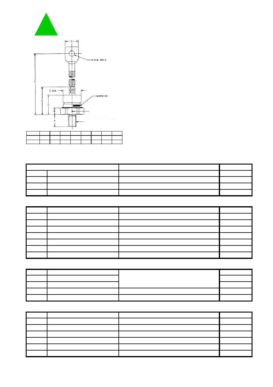
Value
Symbol
A
B
C
D
E
F
G
H
Inches
0.63
0.34
0.98
1.58
0.89
4.48
0.63 0.281
mm
16.0
8.6
24.9
40.1
22.6 113.8
16.0
7.14
Strike distance .64 inch / 16.2 mm (Min)
.375 - 24 UNF - 2A THD.
1.055 inch / 26.8 mm
across flat
Green Power Solutions srl
Via Greto di Cornigliano 6R - 16152 Genova , Italy
Phone: +39-010-659 1869
Fax: +39-010-659 1870
Web: www.gpsemi.it
E-mail: info@gpsemi.it
Green Power
Semiconductors