Rev: 1.15 6/2001
1/34
© 1998, Giga Semiconductor, Inc.
Specifications cited are subject to change without notice. For latest documentation see http://www.gsitechnology.com.
NoBL is a trademark of Cypress Semiconductor Corp.. NtRAM is a trademark of Samsung Electronics Co.. ZBT is a trademark of Integrated Device Technology, Inc.
Preliminary
GS882Z18/36B-11/100/80/66
8Mb Pipelined and Flow Through
Synchronous NBT SRAMs
100 MHz≠66 MHz
3.3 V V
DD
2.5 V and 3.3 V V
DDQ
119-Bump BGA
Commercial Temp
Industrial Temp
Features
∑ 512K x 18 and 256K x 36 configurations
∑ User-configurable Pipelined and Flow Through mode
∑ NBT (No Bus Turn Around) functionality allows zero wait
∑ Read-Write-Read bus utilization
∑ Fully pin-compatible with both pipelined and flow through
NtRAMTM, NoBLTM and ZBTTM SRAMs
∑ IEEE 1149.1 JTAG-compatible Boundary Scan
∑ On-chip write parity checking; even or odd selectable
∑ ZQ mode pin for user selectable high/low output drive
strength.
∑ x16/x32 mode with on-chip parity encoding and error
detection
∑ Pin-compatible with 2M, 4M and 16M devices
∑ 3.3 V +10%/≠5% core power supply
∑ 2.5 V or 3.3 V I/O supply
∑ LBO pin for Linear or Interleave Burst mode
∑ Byte write operation (9-bit Bytes)
∑ 3 chip enable signals for easy depth expansion
∑ Clock Control, registered, address, data, and control
∑ ZZ Pin for automatic power-down
∑ JEDEC-standard 119-Bump BGA package
Functional Description
The GS882Z818/36B is an 8Mbit Synchronous Static SRAM.
GSI's NBT SRAMs, like ZBT, NtRAM, NoBL or other
pipelined read/double late write or flow through read/single
late write SRAMs, allow utilization of all available bus
bandwidth by eliminating the need to insert deselect cycles
when the device is switched from read to write cycles.
Because it is a synchronous device, address, data inputs, and
read/ write control inputs are captured on the rising edge of the
input clock. Burst order control (LBO) must be tied to a power
rail for proper operation. Asynchronous inputs include the
Sleep mode enable (ZZ) and Output Enable. Output Enable can
be used to override the synchronous control of the output
drivers and turn the RAM's output drivers off at any time.
Write cycles are internally self-timed and initiated by the rising
edge of the clock input. This feature eliminates complex off-
chip write pulse generation required by asynchronous SRAMs
and simplifies input signal timing.
The GS882Z818/36B may be configured by the user to
operate in Pipeline or Flow Through mode. Operating as a
pipelined synchronous device, in addition to the rising-edge-
triggered registers that capture input signals, the device
incorporates a rising-edge-triggered output register. For read
cycles, pipelined SRAM output data is temporarily stored by
the edge-triggered output register during the access cycle and
then released to the output drivers at the next rising edge of
clock.
The GS882Z818/36B is implemented with GSI's high
performance CMOS technology and is available in a JEDEC-
Standard 119-bump BGA package.
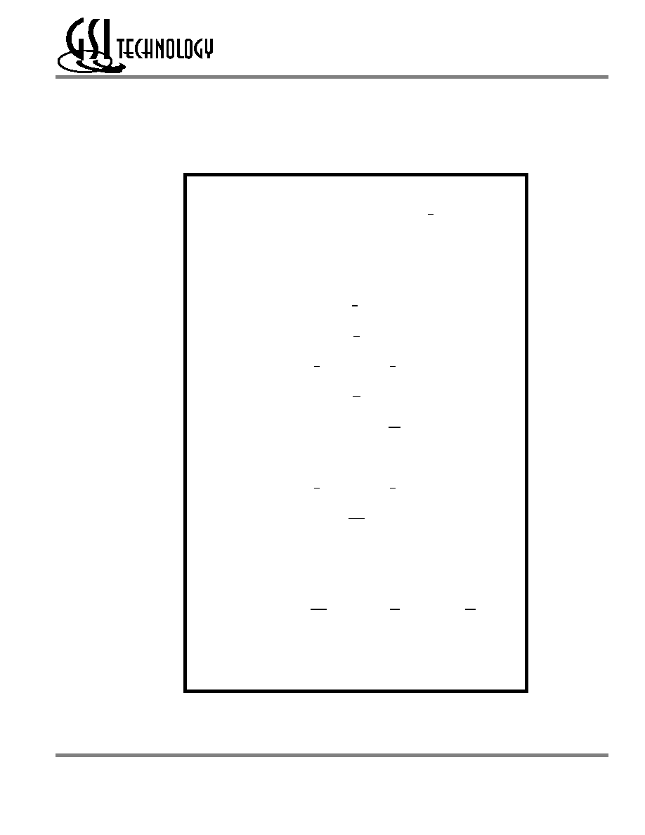
-11
-100
-80
-66
Pipeline
3-1-1-1
t
Cycle
t
KQ
I
DD
10 ns
4.5 ns
210 mA
10 ns
4.5 ns
210 mA
12.5 ns
4.8 ns
190 mA
15 ns
5 ns
170 mA
Flow Through
2-1-1-1
t
KQ
t
Cycle
I
DD
11 ns
15 ns
150 mA
12 ns
15 ns
150 mA
14 ns
15 ns
130 mA
18 ns
20 ns
130 mA
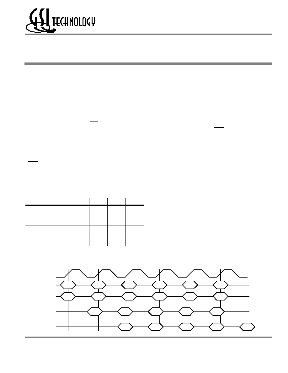
A
B
C
D
E
F
R
W
R
W
R
W
Q
A
D
B
Q
C
D
D
Q
E
Q
A
D
B
Q
C
D
D
Q
E
Clock
Address
Read/Write
Flow Through
Data I/O
Pipelined
Data I/O
Flow Through and Pipelined NBT SRAM Back-to-Back Read/Write Cycles
Rev: 1.15 6/2001
4/34
© 1998, Giga Semiconductor, Inc.
Specifications cited are subject to change without notice. For latest documentation see http://www.gsitechnology.com
Preliminary
.
GS882Z18/36B-11/100/80/66
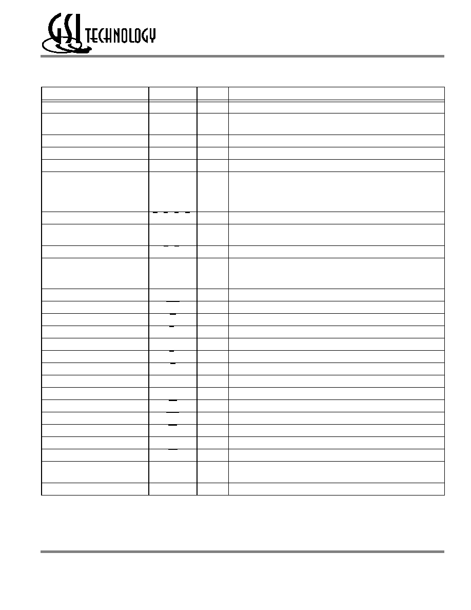
GS882Z18/36 BGA Pin Description
Pin Location
Symbol
Type
Description
P4, N4
A
0
, A
1
I
Address field LSBs and Address Counter Preset Inputs
A2, A3, A5, A6, B3, B5, C2, C3, C5,
C6, G4, R2, R6, T3, T5
An
I
Address Inputs
T4
An
I
Address Inputs (x36 Version)
T2, T6
NC
--
No Connect (x36 Version)
T2, T6
An
I
Address Inputs (x18 Version)
K7, L7, N7, P7, K6, L6, M6, N6, P6
H7, G7, E7, D7, H6, G6, F6, E6, D6
H1, G1, E1, D1, H2, G2, F2, E2, D2
K1, L1, N1, P1, K2, L2, M2, N2, P2
DQ
A1
≠DQ
PA9
DQ
B1
≠DQ
PB9
DQ
C1
≠DQ
PC9
DQ
D1
≠DQ
PD9
I/O
Data Input and Output pins (x36 Version)
L5, G5, G3, L3
B
A
, B
B
, B
C
, B
D
I
Byte Write Enable for DQ
A
, DQ
B
, DQ
C
, DQ
D
I/Os; active low ( x36 Version)
P7, N6, L6, K7, H6, G7, F6, E7, D6
D1, E2, G2, H1, K2, L1, M2, N1, P2
DQ
A1
≠DQ
A9
DQ
B1
≠DQ
B9
I/O
Data Input and Output pins (x18 Version)
L5, G3
B
A
, B
B
I
Byte Write Enable for DQ
A
, DQ
B
Data I/Os; active low ( x18 Version)
P6, N7, M6, L7, K6, H7, G6, E6, D7,
D2, E1, F2, G1, H2, K1, L2, N2, P1,
G5, L3, T4
NC
--
No Connect (x18 Version)
K4
CK
I
Clock Input Signal; active high
M4
CKE
I
Clock Input Buffer Enable; active low
H4
W
I
Write Enable--Writes all enabled bytes; active low
E4
E
1
I
Chip Enable; active low
B2
E
2
I
Chip Enable; active high
B6
E
3
I
Chip Enable; active low
F4
G
I
Output Enable; active low
B4
ADV
I
Burst address counter advance enable; active high
T7
ZZ
I
Sleep Mode control; active high
R5
FT
I
Flow Through or Pipeline mode; active low
R3
LBO
I
Linear Burst Order mode; active low
R7
PE
I
Parity Bit Enable; active low (High = x16/32 Mode, Low = x18/36 Mode)
J3
DP
I
Data Parity Mode Input; 1 = Even, 0 = Odd
J5
QE
O
Parity Error Out; Open Drain Output
D4
ZQ
I
FLXDrive Output Impedance Control
(Low = Low Impedance [High Drive], High = High Impedance [Low Drive])
B1, C1, R1, T1, L4, B7, C7, U6
NC
--
No Connect
Rev: 1.15 6/2001
5/34
© 1998, Giga Semiconductor, Inc.
Specifications cited are subject to change without notice. For latest documentation see http://www.gsitechnology.com
Preliminary
.
GS882Z18/36B-11/100/80/66
BPR2000.002.14
Functional Details
Clocking
Deassertion of the Clock Enable (CKE) input blocks the Clock input from reaching the RAM's internal circuits. It may be used to
suspend RAM operations. Failure to observe Clock Enable set-up or hold requirements will result in erratic operation.
Pipeline Mode Read and Write Operations
All inputs (with the exception of Output Enable, Linear Burst Order and Sleep) are synchronized to rising clock edges. Single cycle
read and write operations must be initiated with the Advance/Load pin (ADV) held low, in order to load the new address. Device
activation is accomplished by asserting all three of the Chip Enable inputs (E
1
, E
2,
and E
3
). Deassertion of any one of the Enable
inputs will deactivate the device.
Read operation is initiated when the following conditions are satisfied at the rising edge of clock: CKE is asserted Low, all three
chip enables (E1, E2, and E3) are active, the write enable input signals W is deasserted high, and ADV is asserted low. The address
presented to the address inputs is latched in to address register and presented to the memory core and control logic. The control
logic determines that a read access is in progress and allows the requested data to propagate to the input of the output register. At
the next rising edge of clock the read data is allowed to propagate through the output register and onto the Output pins.
Write operation occurs when the RAM is selected, CKE is active and the Write input is sampled low at the rising edge of clock.
U2
TMS
I
Scan Test Mode Select
U3
TDI
I
Scan Test Data In
U5
TDO
O
Scan Test Data Out
U4
TCK
I
Scan Test Clock
J2, C4, J4, R4, J6
V
DD
I
Core power supply
D3, E3, F3, H3, K3, M3, N3, P3, D5,
E5, F5, H5, K5, M5, N5, P5
V
SS
I
I/O and Core Ground
A1, F1, J1, M1, U1, A7, F7, J7, M7,
U7
V
DDQ
I
Output driver power supply
Function
W
B
A
B
B
B
C
B
D
Read
H
X
X
X
X
Write Byte "a"
L
L
H
H
H
Write Byte "b"
L
H
L
H
H
Write Byte "c"
L
H
H
L
H
Write Byte "d"
L
H
H
H
L
Write all Bytes
L
L
L
L
L
Write Abort/NOP
L
H
H
H
H
GS882Z18/36 BGA Pin Description
Pin Location
Symbol
Type
Description