Rev: 1.06 6/2000
1/15
© 1999, Giga Semiconductor, Inc.
Specifications cited are subject to change without notice. For latest documentation see http://www.gsitechnology.com.
M
GS71116TP/J/U
64K x 16
1Mb Asynchronous SRAM
10, 12, 15ns
3.3V V
DD
Center V
DD
& V
SS
SOJ, TSOP, FP-BGA
Commercial Temp
Industrial Temp
Features
∑ Fast access time: 10, 12, 15ns
∑ CMOS low power operation: 100/85/70 mA at min. cycle time.
∑ Single 3.3V ± 0.3V power supply
∑ All inputs and outputs are TTL compatible
∑ Byte control
∑ Fully static operation
∑ Industrial Temperature Option: -40∞ to 85∞C
∑ Package line up
J: 400mil, 44 pin SOJ package
TP: 400mil, 44 pin TSOP Type II package
U: 6 mm x 8 mm Fine Pitch Ball Grid Array package
Description
The GS71116 is a high speed CMOS static RAM organized as
65,536-words by 16-bits. Static design eliminates the need for exter-
nal clocks or timing strobes. Operating on a single 3.3V power supply
and all inputs and outputs are TTL compatible. The GS71116 is avail-
able in a 6x8 mm Fine Pitch BGA package as well as in 400 mil SOJ
and 400 mil TSOP Type-II packages.
Pin Descriptions
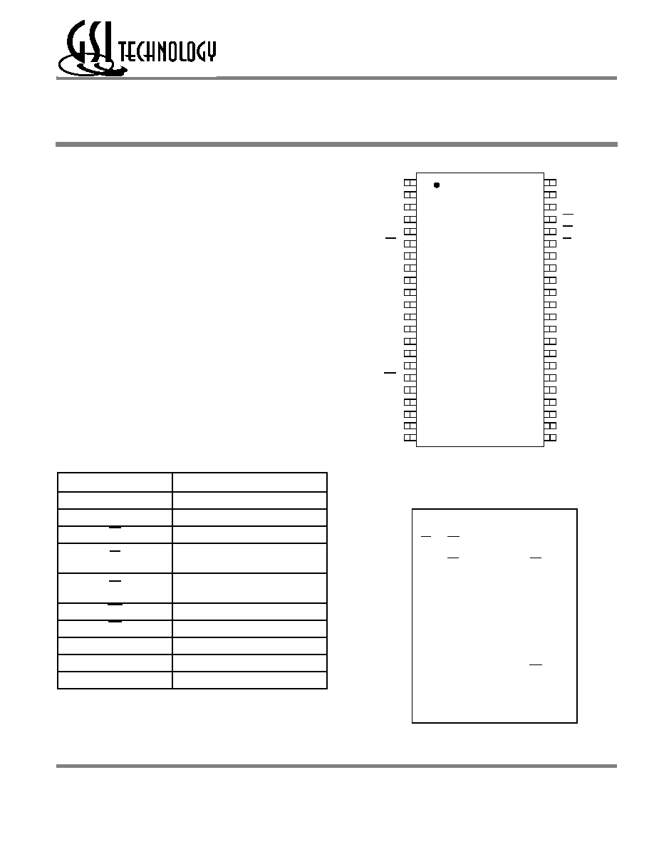
SOJ 64K x 16 Pin Configuration
Fine Pitch BGA 64K x 16 Bump Configuration
6mm x 8mm, 0.75mm Bump Pitch
Top View
Symbol
Description
A
0
to A
15
Address input
DQ
1
to DQ
16
Data input/output
CE
Chip enable input
LB
Lower byte enable input
(DQ1 to DQ8)
UB
Upper byte enable input
(DQ9 to DQ16)
WE
Write enable input
OE
Output enable input
V
DD
+3.3V power supply
V
SS
Ground
NC
No connect
1
2
3
4
5
6
A
LB
OE
A
0
A
1
A
2
NC
B
DQ
16
UB
A
3
A
4
CE
DQ
1
C
DQ
14
DQ
15
A
5
A
6
DQ
2
DQ
3
D
V
SS
DQ
13
NC
A
7
DQ
4
V
DD
E
V
DD
DQ
12
NC
NC
DQ
5
V
SS
F
DQ
11
DQ
10
A
8
A
9
DQ
7
DQ
6
G
DQ
9
NC
A
10
A
11
WE
DQ
8
H
NC
A
12
A
13
A
14
A
15
NC
44
43
42
41
40
39
38
37
36
35
34
33
32
31
30
29
28
27
26
25
1
2
3
4
5
6
7
8
9
10
11
12
13
14
15
16
17
18
19
20
A
4
A
3
A
2
A
1
A
0
CE
DQ
1
DQ
2
DQ
3
DQ
4
V
DD
V
SS
DQ
5
DQ6
DQ7
DQ
8
WE
A
15
A
14
A
13
A
5
A
6
A
7
OE
UB
LB
DQ
16
DQ
15
DQ
14
DQ
13
V
SS
V
DD
DQ
12
DQ
11
DQ
10
DQ
9
NC
A
8
A
9
A
10
Top view
21
22
24
23
A
12
A
11
44 pin
SOJ
NC
NC
Rev: 1.06 6/2000
2/15
© 1999, Giga Semiconductor, Inc.
Specifications cited are subject to change without notice. For latest documentation see http://www.gsitechnology.com.
GS71116TP/J/U
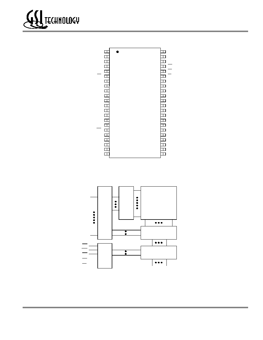
TSOP-II 64K x 16 Pin Configuration
44
43
42
41
40
39
38
37
36
35
34
33
32
31
30
29
28
27
26
25
1
2
3
4
5
6
7
8
9
10
11
12
13
14
15
16
17
18
19
20
A
4
A
3
A
2
A
1
A
0
CE
DQ
1
DQ
2
DQ
3
DQ
4
V
DD
V
SS
DQ
5
DQ
6
DQ
7
DQ
8
WE
A
15
A14
A
13
A
5
A
6
A
7
OE
UB
LB
DQ
16
DQ
15
DQ
14
DQ
13
V
SS
V
DD
DQ
12
DQ
11
DQ
10
DQ
9
NC
A
8
A
9
A
10
Top view
21
22
24
23
A
12
A
11
44 pin
TSOP II
NC
NC
Memory Array
Row
Decoder
Column
Decoder
Address
Input
Buffer
Control
I/O Buffer
A
0
CE
WE
OE
DQ
1
A
15
Block Diagram
DQ
16
UB _____
LB _____
Rev: 1.06 6/2000
3/15
© 1999, Giga Semiconductor, Inc.
Specifications cited are subject to change without notice. For latest documentation see http://www.gsitechnology.com.
GS71116TP/J/U
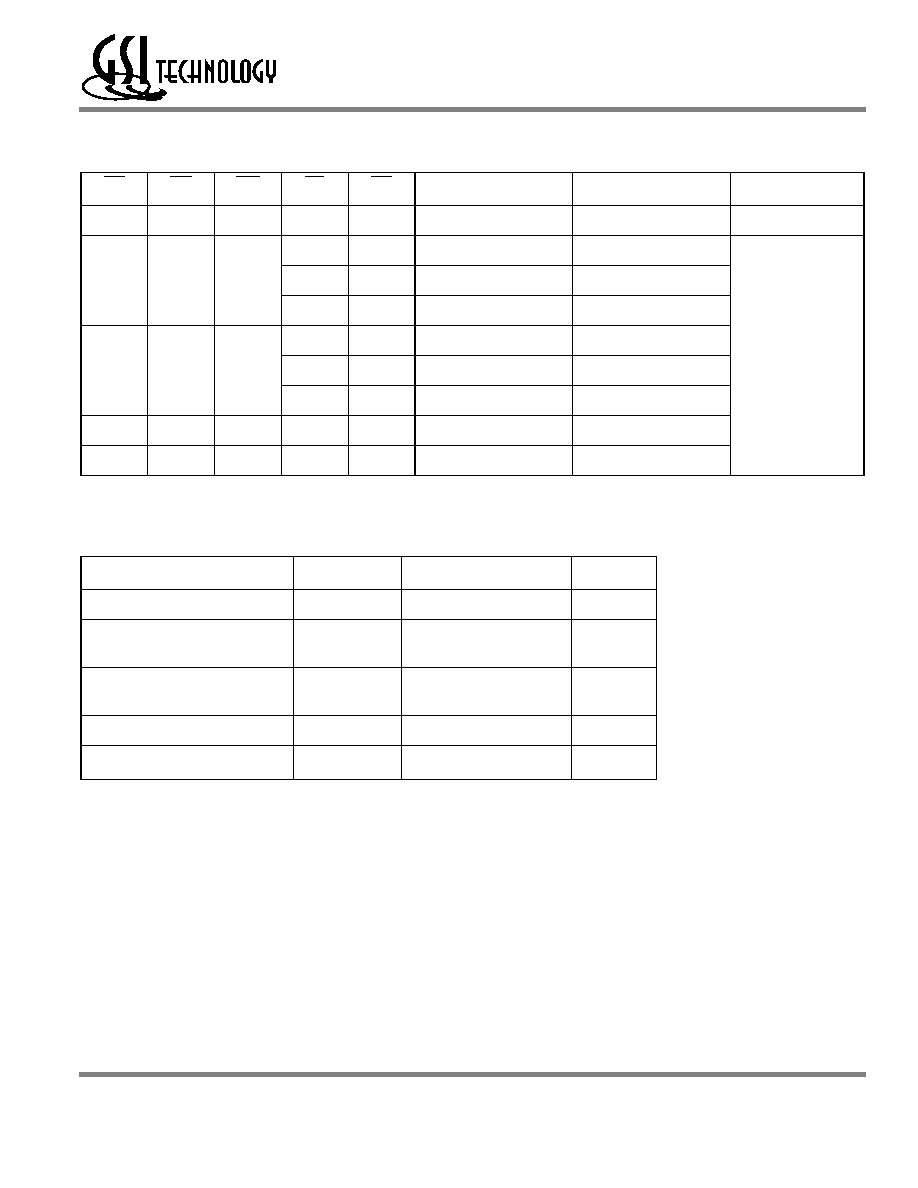
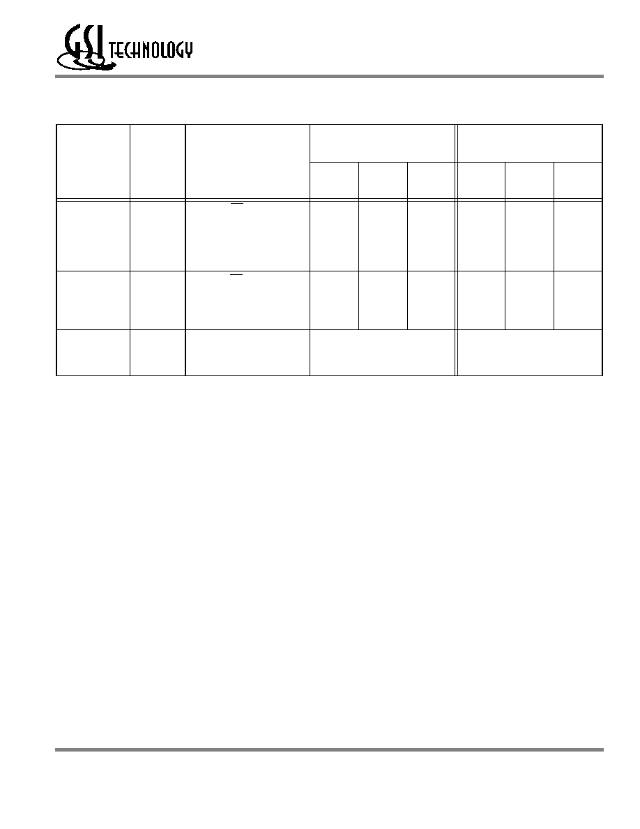
Note: X: "H" or "L"
Note:
Permanent device damage may occur if Absolute Maximum Ratings are exceeded. Functional operation shall be restricted to Recommended
Operating Conditions. Exposure to higher than recommended voltages for extended periods of time could affect device reliability.
Truth Table
CE
OE
WE
LB
UB
DQ
1
to DQ
8
DQ
9
to DQ
16
V
DD
Current
H
X
X
X
X
Not Selected
Not Selected
ISB
1
, ISB
2
L
L
H
L
L
Read
Read
I
DD
L
H
Read
High Z
H
L
High Z
Read
L
X
L
L
L
Write
Write
L
H
Write
Not Write, High Z
H
L
Not Write, High Z
Write
L
H
H
X
X
High Z
High Z
L
X
X
H
H
High Z
High Z
Absolute Maximum Ratings
Parameter
Symbol
Rating
Unit
Supply Voltage
V
DD
-0.5 to +4.6
V
Input Voltage
V
IN
-0.5 to V
DD
+0.5
(
4.6V max.)
V
Output Voltage
V
OUT
-0.5 to V
DD
+0.5
(
4.6V max.)
V
Allowable power dissipation
PD
0.7
W
Storage temperature
T
STG
-55 to 150
o
C
Rev: 1.06 6/2000
4/15
© 1999, Giga Semiconductor, Inc.
Specifications cited are subject to change without notice. For latest documentation see http://www.gsitechnology.com.
GS71116TP/J/U
Note:
1. Input overshoot voltage should be less than V
DD
+2V and not exceed 20ns.
2. Input undershoot voltage should be greater than -2V and not exceed 20ns.
Notes:
1. Tested at T
A
=25∞C, f=1MHz
2. These parameters are sampled and are not 100% tested
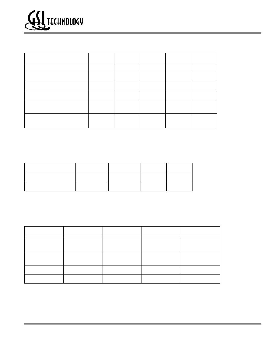
Recommended Operating Conditions
Parameter
Symbol
Min
Typ
Max
Unit
Supply Voltage for -12/15
V
DD
3.0
3.3
3.6
V
Supply Voltage for -10
V
DD
3.135
3.3
3.6
V
Input High Voltage
V
IH
2.0
-
V
DD
+0.3
V
Input Low Voltage
V
IL
-0.3
-
0.8
V
Ambient Temperature,
Commercial Range
T
Ac
0
-
70
o
C
Ambient Temperature,
Industrial Range
T
A
I
-40
-
85
o
C
Capacitance
Parameter
Symbol
Test Condition
Max
Unit
Input Capacitance
C
IN
V
IN
=0V
5
pF
Output Capacitance
C
OUT
V
OUT
=0V
7
pF
DC I/O Pin Characteristics
Parameter
Symbol
Test Conditions
Min
Max
Input Leakage
Current
I
IL
V
IN
= 0 to V
DD
-1uA
1uA
Output Leakage
Current
I
LO
Output High Z
V
OUT
= 0 to V
DD
-1uA
1uA
Output High Voltage
V
OH
I
OH
= - 4mA
2.4
Output Low Voltage
V
OL
I
LO
= + 4mA
0.4V
Rev: 1.06 6/2000
5/15
© 1999, Giga Semiconductor, Inc.
Specifications cited are subject to change without notice. For latest documentation see http://www.gsitechnology.com.
GS71116TP/J/U
Power Supply Currents
Parameter
Symbol
Test Conditions
0 to 70∞C
-40 to 85∞C
10ns
12ns
15ns
10ns
12ns
15ns
Operating
Supply
Current
I
DD
(max)
CE
V
IL
All other inputs
V
IH
or
V
IL
Min. cycle time
I
OUT
= 0 mA
100mA
85mA
70mA
115mA
100mA
85mA
Standby
Current
I
SB1
(max)
CE
V
IH
All other inputs
V
IH
or
V
IL
Min. cycle time
45mA
40mA
35mA
50mA
45mA
40mA
Standby
Current
I
SB2
(max)
CE
V
DD
- 0.2V
All other inputs
V
DD
- 0.2V or
0.2V
10mA
15mA