Rev: 1.03 10/2002
1/14
© 2001, Giga Semiconductor, Inc.
Specifications cited are subject to change without notice. For latest documentation see http://www.gsitechnology.com.
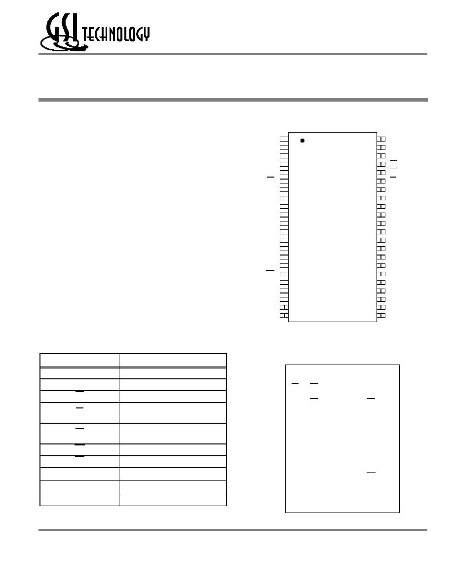
GS74116ATP/J/X
256K x 16
4Mb Asynchronous SRAM
7, 8, 10, 12 ns
3.3 V V
DD
Center V
DD
and V
SS
SOJ, TSOP, FP-BGA
Commercial Temp
Industrial Temp
Features
∑ Fast access time: 7, 8, 10, 12 ns
∑ CMOS low power operation: 150/130/105/95 mA at
minimum cycle time
∑ Single 3.3 V power supply
∑ All inputs and outputs are TTL-compatible
∑ Byte control
∑ Fully static operation
∑ Industrial Temperature Option: ≠40∞ to 85∞C
∑ Package line up
J: 400 mil, 44-pin SOJ package
TP: 400 mil, 44-pin TSOP Type II package
X: 6 mm x 10 mm Fine Pitch Ball Grid Array
package
Description
The GS74116A is a high speed CMOS Static RAM organized
as 262,144 words by 16 bits. Static design eliminates the need
for external clocks or timing strobes. The GS operates on a
single 3.3 V power supply and all inputs and outputs are TTL-
compatible. The GS74116A is available in a 6 x 10 mm Fine
Pitch BGA package, 400 mil SOJ and 400 mil TSOP Type-II
packages.
Pin Descriptions
SOJ 256K x 16-Pin Configuration (Package J)
FP-BGA 256K x 16 Bump Configuration (Package X)
6 x 10 mm Bump Pitch
Symbol
Description
A
0
≠A
17
Address input
DQ
1
≠DQ
16
Data input/output
CE
Chip enable input
LB
Lower byte enable input
(DQ1 to DQ8)
UB
Upper byte enable input
(DQ9 to DQ16)
WE
Write enable input
OE
Output enable input
V
DD
+3.3 V power supply
V
SS
Ground
NC
No connect
1
2
3
4
5
6
A
LB
OE
A
0
A
1
A
2
NC
B
DQ
16
UB
A
3
A
4
CE
DQ
1
C
DQ
14
DQ
15
A
5
A
6
DQ
2
DQ
3
D
V
SS
DQ
13
A
17
A
7
DQ
4
V
DD
E
V
DD
DQ
12
NC
A
16
DQ
5
V
SS
F
DQ
11
DQ
10
A
8
A
9
DQ
7
DQ
6
G
DQ
9
NC
A
10
A
11
WE
DQ
8
H
NC
A
12
A
13
A
14
A
15
NC
44
43
42
41
40
39
38
37
36
35
34
33
32
31
30
29
28
27
26
25
1
2
3
4
5
6
7
8
9
10
11
12
13
14
15
16
17
18
19
20
A
4
A
3
A
2
A
1
A
0
CE
DQ
1
DQ
2
DQ
3
DQ
4
V
DD
V
SS
DQ
5
DQ6
DQ7
DQ
8
WE
A
15
A
14
A
13
A
5
A
6
A
7
OE
UB
LB
DQ
16
DQ
15
DQ
14
DQ
13
V
SS
V
DD
DQ
12
DQ
11
DQ
10
DQ
9
NC
A
8
A
9
A
10
Top view
21
22
24
23
A
12
A
11
44-pin
SOJ
A
17
A
16
Rev: 1.03 10/2002
2/14
© 2001, Giga Semiconductor, Inc.
Specifications cited are subject to change without notice. For latest documentation see http://www.gsitechnology.com.
GS74116ATP/J/X
Top View
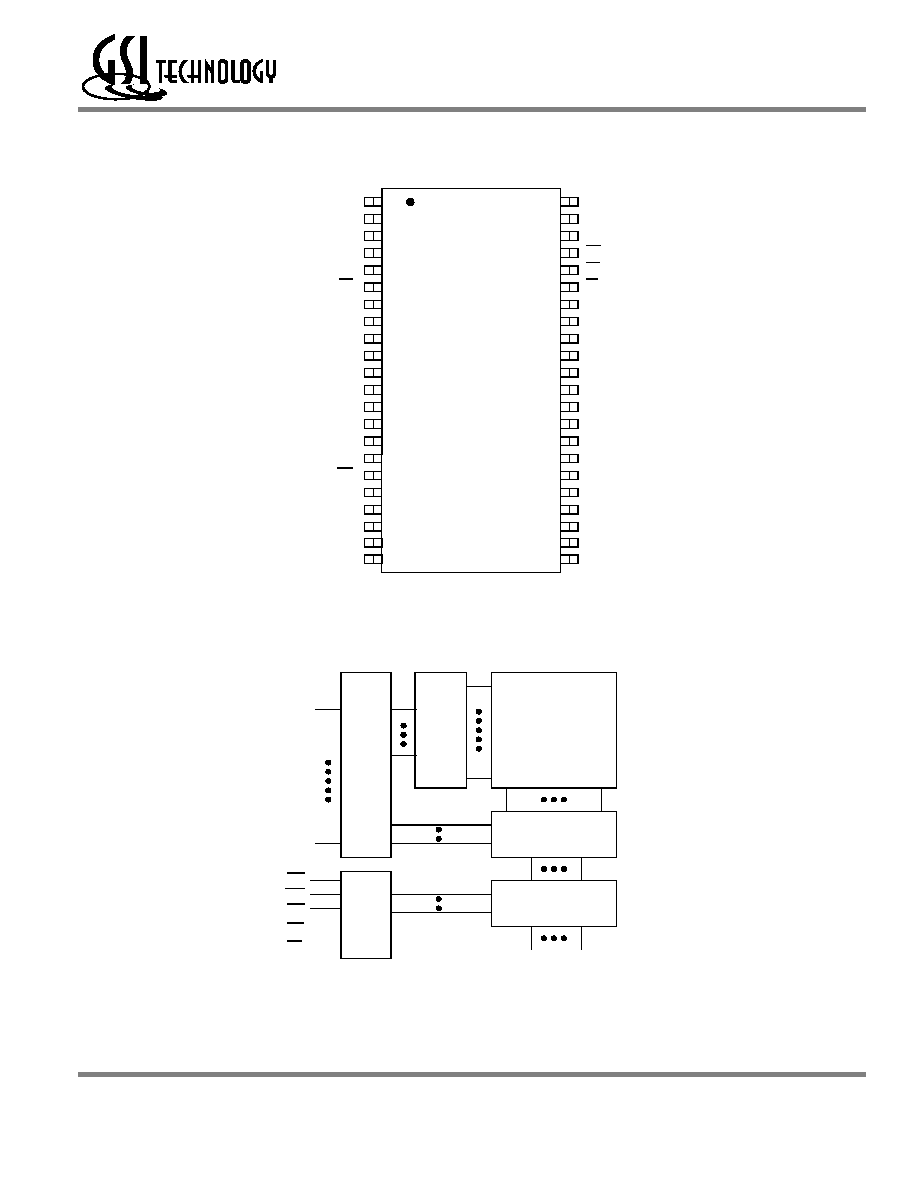
TSOP-II 256K x 16 Pin Configuration (Package TP)
44
43
42
41
40
39
38
37
36
35
34
33
32
31
30
29
28
27
26
25
1
2
3
4
5
6
7
8
9
10
11
12
13
14
15
16
17
18
19
20
A
4
A
3
A
2
A
1
A
0
CE
DQ
1
DQ
2
DQ
3
DQ
4
V
DD
V
SS
DQ
5
DQ
6
DQ
7
DQ
8
WE
A
15
A14
A
13
A
5
A
6
A
7
OE
UB
LB
DQ
16
DQ
15
DQ
14
DQ
13
V
SS
V
DD
DQ
12
DQ
11
DQ
10
DQ
9
NC
A
8
A
9
A
10
Top view
21
22
24
23
A
12
A
11
44 pin
TSOP II
A
17
A
16
Memory Array
Row
Decoder
Column
Decoder
Address
Input
Buffer
Control
I/O Buffer
A
0
CE
WE
OE
DQ
1
A
17
Block Diagram
DQ
16
UB _____
LB _____
Rev: 1.03 10/2002
3/14
© 2001, Giga Semiconductor, Inc.
Specifications cited are subject to change without notice. For latest documentation see http://www.gsitechnology.com.
GS74116ATP/J/X
Note: X: "H" or "L"
Note:
Permanent device damage may occur if Absolute Maximum Ratings are exceeded. Functional operation shall be restricted to Rec-
ommended Operating Conditions. Exposure to higher than recommended voltages for extended periods of time could affect device
reliability.
Truth Table
CE
OE
WE
LB
UB
DQ
1
to DQ
8
DQ
9
to DQ
16
V
DD
Current
H
X
X
X
X
Not Selected
Not Selected
ISB
1
, ISB
2
L
L
H
L
L
Read
Read
I
DD
L
H
Read
High Z
H
L
High Z
Read
L
X
L
L
L
Write
Write
L
H
Write
Not Write, High Z
H
L
Not Write, High Z
Write
L
H
H
X
X
High Z
High Z
L
X
X
H
H
High Z
High Z
Absolute Maximum Ratings
Parameter
Symbol
Rating
Unit
Supply Voltage
V
DD
≠0.5 to +4.6
V
Input Voltage
V
IN
≠0.5 to V
DD
+0.5
(
4.6 V max.)
V
Output Voltage
V
OUT
≠0.5 to V
DD
+0.5
(
4.6 V max.)
V
Allowable power dissipation
PD
0.7
W
Storage temperature
T
STG
≠55 to 150
o
C
Rev: 1.03 10/2002
4/14
© 2001, Giga Semiconductor, Inc.
Specifications cited are subject to change without notice. For latest documentation see http://www.gsitechnology.com.
GS74116ATP/J/X
Note:
1. Input overshoot voltage should be less than V
DD
+2 V and not exceed 20 ns.
2. Input undershoot voltage should be greater than ≠2 V and not exceed 20 ns.
Notes:
1. Tested at T
A
= 25∞C, f = 1 MHz
2. These parameters are sampled and are not 100% tested.
Recommended Operating Conditions
Parameter
Symbol
Min
Typ
Max
Unit
Supply Voltage for -7/-8/-10/-12
V
DD
3.0
3.3
3.6
V
Input High Voltage
V
IH
2.0
--
V
DD
+0.3
V
Input Low Voltage
V
IL
≠0.3
--
0.8
V
Ambient Temperature,
Commercial Range
T
Ac
0
--
70
o
C
Ambient Temperature,
Industrial Range
T
A
I
≠40
--
85
o
C
Capacitance
Parameter
Symbol
Test Condition
Max
Unit
Input Capacitance
C
IN
V
IN
= 0 V
5
pF
Output Capacitance
C
OUT
V
OUT
= 0 V
7
pF
DC I/O Pin Characteristics
Parameter
Symbol
Test Conditions
Min
Max
Input Leakage
Current
I
IL
V
IN
= 0 to V
DD
≠ 1 uA
1 uA
Output Leakage
Current
I
LO
Output High Z
V
OUT
= 0 to V
DD
≠1 uA
1 uA
Output High Voltage
V
OH
I
OH
= ≠4 mA
2.4
--
Output Low Voltage
V
OL
I
LO
= +4 mA
--
0.4 V
Rev: 1.03 10/2002
5/14
© 2001, Giga Semiconductor, Inc.
Specifications cited are subject to change without notice. For latest documentation see http://www.gsitechnology.com.
GS74116ATP/J/X
AC Test Conditions
Power Supply Currents
Parameter
Symbol
Test Conditions
0 to 70∞C
≠40 to 85∞C
Unit
7 ns
8 ns
10 ns
12 ns
7 ns
8 ns
10 ns
12 ns
Operating
Supply
Current
I
DD
CE
V
IL
All other inputs
V
IH
or
V
IL
Min. cycle time
I
OUT
= 0 mA
150
130 105 90 160
140 115 100 mA
Standby
Current
I
SB1
CE
V
IH
All other inputs
V
IH
or
V
IL
Min. cycle time
40
30 25 25 50
40 35 35 mA
Standby
Current
I
SB2
CE
V
DD
≠ 0.2V
All other inputs
V
DD
≠ 0.2 V or
0.2 V
10
20
mA
DQ
VT = 1.4 V
50
30pF
1
DQ
3.3 V
Output Load 1
Output Load 2
589
434
5pF
1
Note:
1. Include scope and jig capacitance.
2. Test conditions as specified with output loading as shown in Fig. 1
unless otherwise noted.
3. Output load 2 for t
LZ
, t
HZ
, t
OLZ
and t
OHZ
Parameter
Conditions
Input high level
V
IH
= 2.4 V
Input low level
V
IL
= 0.4 V
Input rise time
tr = 1 V/ns
Input fall time
tf = 1 V/ns
Input reference level
1.4 V
Output reference level
1.4 V
Output load
Fig. 1& 2