
Rev: 1.02 10/2002
1/12
© 2001, Giga Semiconductor, Inc.
Specifications cited are subject to change without notice. For latest documentation see http://www.gsitechnology.com.
GS74117AX
256K x 16
4Mb Asynchronous SRAM
7, 8, 10, 12 ns
3.3 V V
DD
Center V
DD
and V
SS
FP-BGA
Commercial Temp
Industrial Temp
Features
∑ Fast access time: 7, 8, 10, 12 ns
∑ CMOS low power operation: 150/130/105/95 mA at
minimum cycle time
∑ Single 3.3 V power supply
∑ All inputs and outputs are TTL-compatible
∑ Byte control
∑ Fully static operation
∑ Industrial Temperature Option: ≠40∞ to 85∞C
∑ Package:
X: 6 mm x 10 mm Fine Pitch Ball Grid Array
package
Description
The GS74117A is a high speed CMOS Static RAM organized
as 262,144 words by 16 bits. Static design eliminates the need
for external clocks or timing strobes. The GS operates on a
single 3.3 V power supply and all inputs and outputs are TTL-
compatible. The GS74117A is available in a 6 x 10 mm Fine
Pitch BGA package.
Pin Descriptions
Fine Pitch BGA 256K x 16 Bump Configuration
Package X
6 x 10 mm Bump Pitch
Top View
Symbol
Description
A
0
≠A
17
Address input
DQ
1
≠DQ
16
Data input/output
CE
Chip enable input
LB
Lower byte enable input
(DQ1 to DQ8)
UB
Upper byte enable input
(DQ9 to DQ16)
WE
Write enable input
OE
Output enable input
V
DD
+3.3 V power supply
V
SS
Ground
NC
No connect
1
2
3
4
5
6
A
LB
OE
A
0
A
1
A
2
NC
B
DQ
1
UB
A
3
A
4
CE
DQ
16
C
DQ
3
DQ
2
A
5
A
6
DQ
15
DQ
14
D
V
SS
DQ
4
A
17
A
7
DQ
13
V
DD
E
V
DD
DQ
5
NC
A
16
DQ
12
V
SS
F
DQ
6
DQ
7
A
8
A
9
DQ
10
DQ
11
G
DQ
8
NC
A
10
A
11
WE
DQ
9
H
NC
A
12
A
13
A
14
A
15
NC

Rev: 1.02 10/2002
2/12
© 2001, Giga Semiconductor, Inc.
Specifications cited are subject to change without notice. For latest documentation see http://www.gsitechnology.com.
GS74117AX
Note: X: "H" or "L"
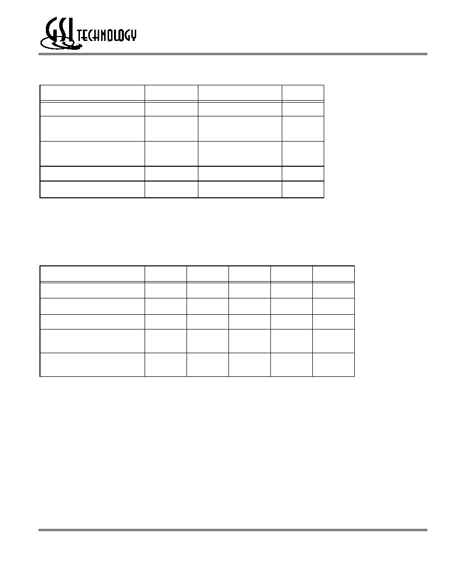
Truth Table
CE
OE
WE
LB
UB
DQ
1
to DQ
8
DQ
9
to DQ
16
V
DD
Current
H
X
X
X
X
Not Selected
Not Selected
ISB
1
, ISB
2
L
L
H
L
L
Read
Read
I
DD
L
H
Read
High Z
H
L
High Z
Read
L
X
L
L
L
Write
Write
L
H
Write
Not Write, High Z
H
L
Not Write, High Z
Write
L
H
H
X
X
High Z
High Z
L
X
X
H
H
High Z
High Z
Memory Array
Row
Decoder
Column
Decoder
Address
Input
Buffer
Control
I/O Buffer
A
0
CE
WE
OE
DQ
1
A
17
Block Diagram
DQ
16
UB _____
LB _____
Rev: 1.02 10/2002
3/12
© 2001, Giga Semiconductor, Inc.
Specifications cited are subject to change without notice. For latest documentation see http://www.gsitechnology.com.
GS74117AX
Note:
Permanent device damage may occur if Absolute Maximum Ratings are exceeded. Functional operation shall be restricted to Rec-
ommended Operating Conditions. Exposure to higher than recommended voltages for extended periods of time could affect device
reliability.
Notes:
1. Input overshoot voltage should be less than V
DD
+2 V and not exceed 20 ns.
2. Input undershoot voltage should be greater than ≠2 V and not exceed 20 ns.
Absolute Maximum Ratings
Parameter
Symbol
Rating
Unit
Supply Voltage
V
DD
≠0.5 to +4.6
V
Input Voltage
V
IN
≠0.5 to V
DD
+0.5
(
4.6 V max.)
V
Output Voltage
V
OUT
≠0.5 to V
DD
+0.5
(
4.6 V max.)
V
Allowable power dissipation
PD
0.7
W
Storage temperature
T
STG
≠55 to 150
o
C
Recommended Operating Conditions
Parameter
Symbol
Min
Typ
Max
Unit
Supply Voltage for -7/-8/-10/-12
V
DD
3.0
3.3
3.6
V
Input High Voltage
V
IH
2.0
--
V
DD
+0.3
V
Input Low Voltage
V
IL
≠0.3
--
0.8
V
Ambient Temperature,
Commercial Range
T
Ac
0
--
70
o
C
Ambient Temperature,
Industrial Range
T
A
I
≠40
--
85
o
C
Rev: 1.02 10/2002
4/12
© 2001, Giga Semiconductor, Inc.
Specifications cited are subject to change without notice. For latest documentation see http://www.gsitechnology.com.
GS74117AX
Notes:
1. Tested at T
A
= 25∞C, f = 1 MHz
2. These parameters are sampled and are not 100% tested.
Capacitance
Parameter
Symbol
Test Condition
Max
Unit
Input Capacitance
C
IN
V
IN
= 0 V
5
pF
Output Capacitance
C
OUT
V
OUT
= 0 V
7
pF
DC I/O Pin Characteristics
Parameter
Symbol
Test Conditions
Min
Max
Input Leakage
Current
I
IL
V
IN
= 0 to V
DD
≠ 1 uA
1 uA
Output Leakage
Current
I
LO
Output High Z
V
OUT
= 0 to V
DD
≠1 uA
1 uA
Output High Voltage
V
OH
I
OH
= ≠4 mA
2.4
--
Output Low Voltage
V
OL
I
LO
= +4 mA
--
0.4 V
Power Supply Currents
Parameter
Symbol
Test Conditions
0 to 70∞C
≠40 to 85∞C
Unit
7 ns
8 ns
10 ns
12 ns
7 ns
8 ns
10 ns
12 ns
Operating
Supply
Current
I
DD
CE
V
IL
All other inputs
V
IH
or
V
IL
Min. cycle time
I
OUT
= 0 mA
150
130 105 90 160
140 115 100 mA
Standby
Current
I
SB1
CE
V
IH
All other inputs
V
IH
or
V
IL
Min. cycle time
28
30 25 22 38
40 35 32 mA
Standby
Current
I
SB2
CE
V
DD
≠ 0.2 V
All other inputs
V
DD
≠ 0.2 V or
0.2 V
10
20
mA
Rev: 1.02 10/2002
5/12
© 2001, Giga Semiconductor, Inc.
Specifications cited are subject to change without notice. For latest documentation see http://www.gsitechnology.com.
GS74117AX
AC Test Conditions
DQ
VT = 1.4 V
50
30pF
1
DQ
3.3 V
Output Load 1
Output Load 2
589
434
5pF
1
Note:
1. Include scope and jig capacitance.
2. Test conditions as specified with output loading as shown in Fig. 1
unless otherwise noted.
3. Output load 2 for t
LZ
, t
HZ
, t
OLZ
and t
OHZ
Parameter
Conditions
Input high level
V
IH
= 2.4 V
Input low level
V
IL
= 0.4 V
Input rise time
tr = 1 V/ns
Input fall time
tf = 1 V/ns
Input reference level
1.4 V
Output reference level
1.4 V
Output load
Fig. 1& 2
Rev: 1.02 10/2002
6/12
© 2001, Giga Semiconductor, Inc.
Specifications cited are subject to change without notice. For latest documentation see http://www.gsitechnology.com.
GS74117AX
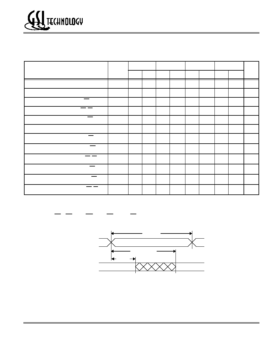
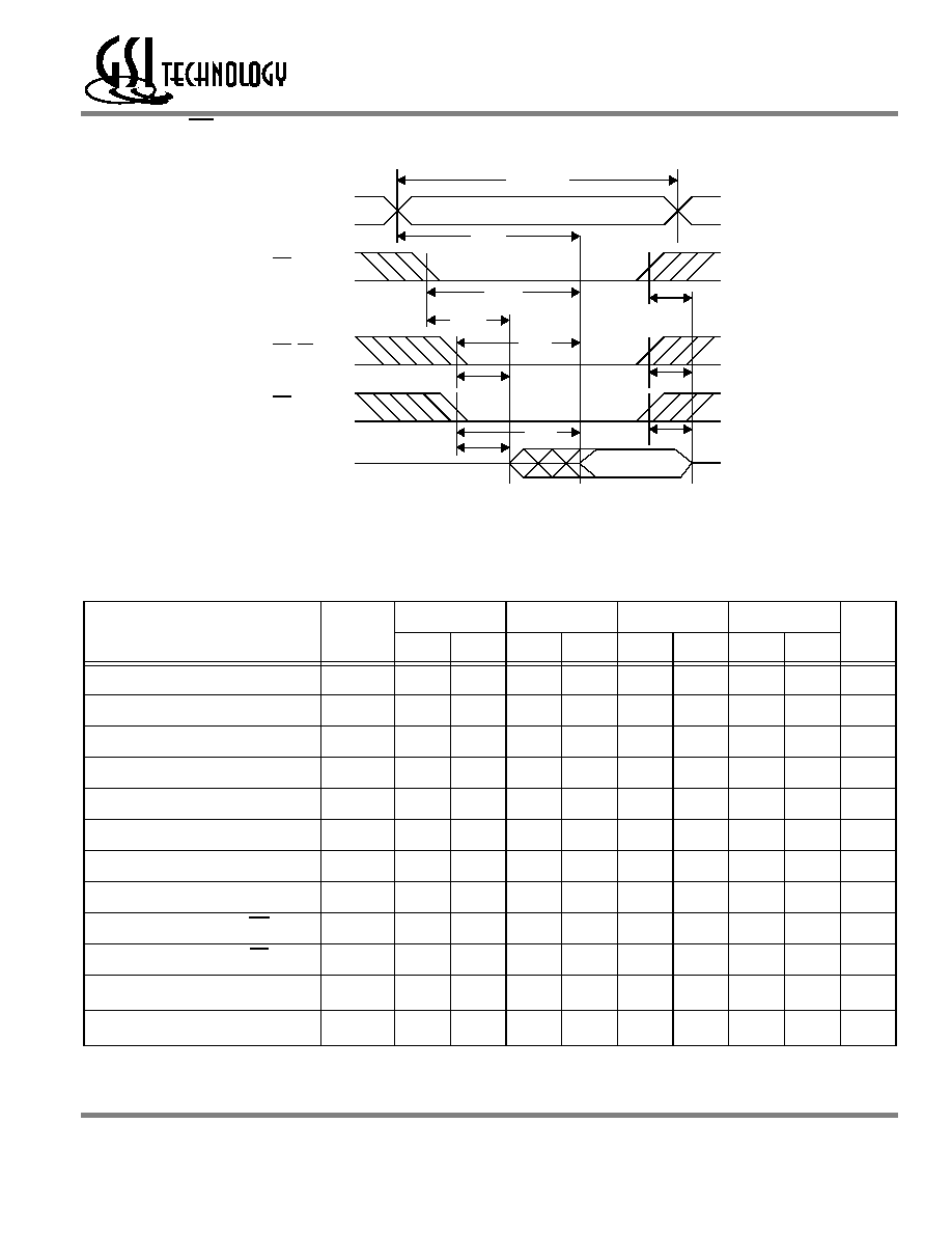
AC Characteristics
* These parameters are sampled and are not 100% tested.
Read Cycle 1: CE = OE = V
IL
, WE = V
IH
, UB and, or LB = V
IL
Read Cycle
Parameter
Symbol
-7
-8
-10
-12
Unit
Min
Max
Min
Max
Min
Max
Min
Max
Read cycle time
t
RC
7
--
8
--
10
--
12
--
ns
Address access time
t
AA
--
7
--
8
--
10
--
12
ns
Chip enable access time (CE)
t
AC
--
7
--
8
--
10
--
12
ns
Byte enable access time (UB, LB)
t
AB
--
3
--
3.5
--
4
--
5
ns
Output enable to output valid (OE)
t
OE
--
3
--
3.5
--
4
--
5
ns
Output hold from address change
t
OH
3
--
3
--
3
--
3
--
ns
Chip enable to output in low Z (CE)
t
LZ
*
3
--
3
--
3
--
3
--
ns
Output enable to output in low Z (OE)
t
OLZ
*
0
--
0
--
0
--
0
--
ns
Byte enable to output in low Z (UB, LB)
t
BLZ
*
0
--
0
--
0
--
0
--
ns
Chip disable to output in High Z (CE)
t
HZ
*
--
3.5
--
4
--
5
--
6
ns
Output disable to output in High Z (OE)
t
OHZ
*
--
3
--
3.5
--
4
--
5
ns
Byte disable to output in High Z (UB, LB)
t
BHZ
*
--
3
--
3.5
--
4
--
5
ns
t
AA
t
OH
t
RC
Address
Data Out
Previous Data
Data valid
Rev: 1.02 10/2002
7/12
© 2001, Giga Semiconductor, Inc.
Specifications cited are subject to change without notice. For latest documentation see http://www.gsitechnology.com.
GS74117AX
Read Cycle 2: WE = V
IH
* These parameters are sampled and are not 100% tested.
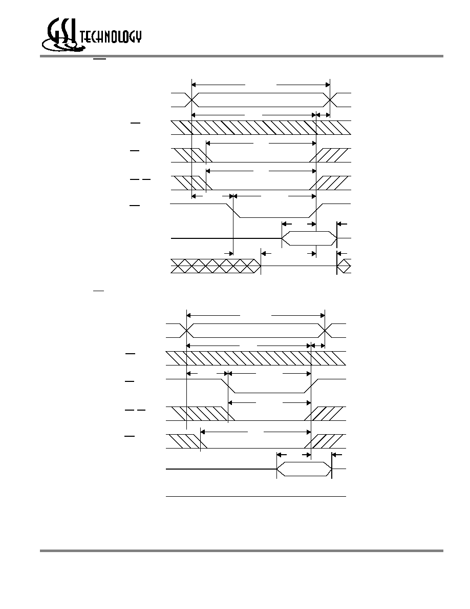
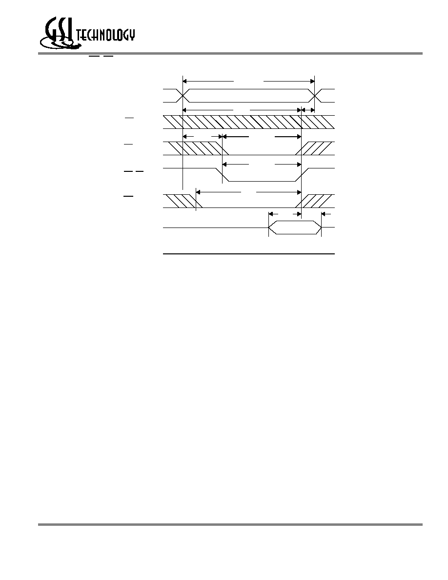
Write Cycle
Parameter
Symbol
-7
-8
-10
-12
Unit
Min
Max
Min
Max
Min
Max
Min
Max
Write cycle time
tWC
7
--
8
--
10
--
12
--
ns
Address valid to end of write
tAW
5
--
5.5
--
7
--
8
--
ns
Chip enable to end of write
tCW
5
--
5.5
--
7
--
8
--
ns
Byte enable to end of write
tBW
5
--
5.5
--
7
--
8
--
ns
Data set up time
tDW
3.5
--
4
--
4.5
--
6
--
ns
Data hold time
tDH
0
--
0
--
0
--
0
--
ns
Write pulse width
tWP
5
--
5.5
--
7
--
8
--
ns
Address set up time
tAS
0
--
0
--
0
--
0
--
ns
Write recovery time (WE)
tWR
0
--
0
--
0
--
0
--
ns
Write recovery time (CE)
tWR1
0
--
0
--
0
--
0
--
ns
Output Low Z from end of write
tWLZ
*
3
--
3
--
3
--
3
--
ns
Write to output in High Z
tWHZ
*
--
3
--
3.5
--
4
--
5
ns
tAA
tRC
Address
tAC
tLZ
tAB
tBLZ
tOE
tOLZ
CE
UB, LB
OE
Data Out
tHZ
tBHZ
tOHZ
Data valid
High impedance
Rev: 1.02 10/2002
8/12
© 2001, Giga Semiconductor, Inc.
Specifications cited are subject to change without notice. For latest documentation see http://www.gsitechnology.com.
GS74117AX
Write Cycle 1: WE control
Write Cycle 2: CE control
tWC
Address
CE
UB, LB
WE
Data In
OE
Data Out
tAW
tCW
tBW
tAS
tWP
tWR
tDW
tDH
tWLZ
tWHZ
Data valid
High impedance
tWC
Address
CE
UB, LB
WE
Data In
OE
Data Out
tAW
tWP
tAS
tCW
tWR1
tDW
tDH
Data valid
High impedance
tBW
Rev: 1.02 10/2002
9/12
© 2001, Giga Semiconductor, Inc.
Specifications cited are subject to change without notice. For latest documentation see http://www.gsitechnology.com.
GS74117AX
Write Cycle 3: UB, LB control
tWC
Address
CE
UB, LB
WE
Data In
OE
Data Out
tAW
tWP
tAS
tCW
tWR1
tDW
tDH
Data valid
High impedance
tBW
Rev: 1.02 10/2002
10/12
© 2001, Giga Semiconductor, Inc.
Specifications cited are subject to change without notice. For latest documentation see http://www.gsitechnology.com.
GS74117AX
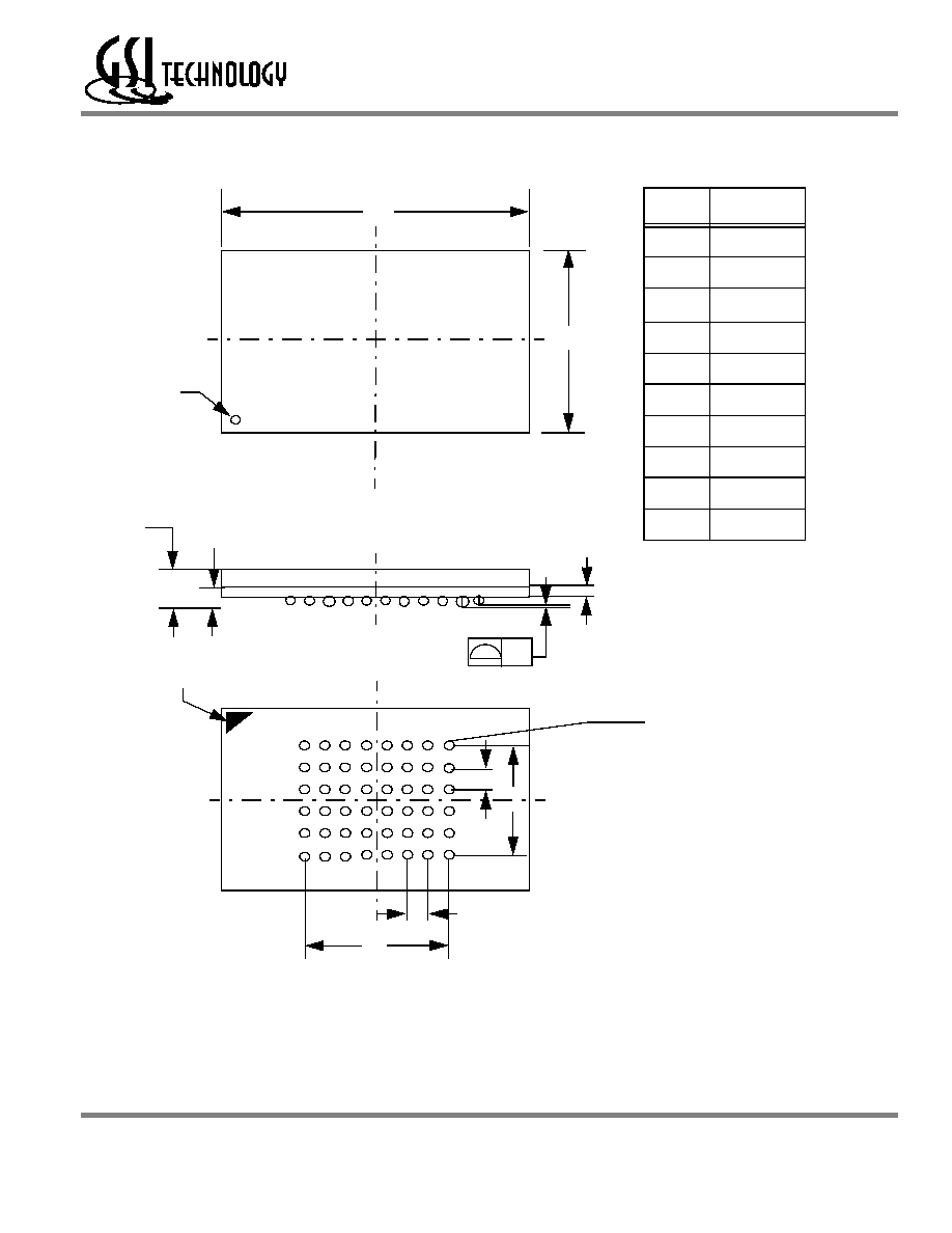
Package X--6 mm x 10 mm FP-BGA
Pin A1
Index
A1
E
Top View
Side View
D
A
aaa
Pin A1
Index
E1
Bottom View
D1
c
e
e
Solder Ball
fb
Symbol
Unit: mm
A
1.10±0.10
A1
0.20~0.30
f
b
f
0.30~0.40
c
0.36(TYP)
D
10.0±0.05
D1
5.25
E
6.0±0.05
E1
3.75
e
0.75(TYP)
aaa
0.10
A B C D E F G H
1
2
3
4
5
6
Rev: 1.02 10/2002
11/12
© 2001, Giga Semiconductor, Inc.
Specifications cited are subject to change without notice. For latest documentation see http://www.gsitechnology.com.
GS74117AX
*
Customers requiring delivery in Tape and Reel should add the character "T" to the end of the part number. For example:
GS74117AX-8T
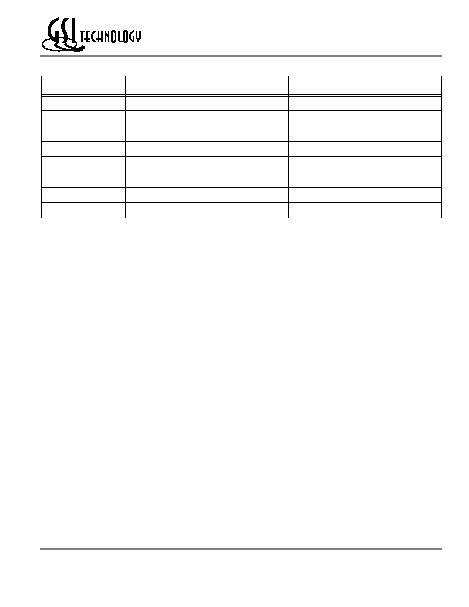
Ordering Information
Part Number
*
Package
Access Time
Temp. Range
Status
GS74117AX-7
6 mm x 10 mm BGA
7 ns
Commercial
GS74117AX-8
6 mm x 10 mm BGA
8 ns
Commercial
GS74117AX-10
6 mm x 10 mm BGA
10 ns
Commercial
GS74117AX-12
6 mm x 10 mm BGA
12 ns
Commercial
GS74117AX-7I
6 mm x 10 mm BGA
7 ns
Industrial
GS74117AX-8I
6 mm x 10 mm BGA
8 ns
Industrial
GS74117AX-10I
6 mm x 10 mm BGA
10 ns
Industrial
GS74117AX-12I
6 mm x 10 mm BGA
12 ns
Industrial

Rev: 1.02 10/2002
12/12
© 2001, Giga Semiconductor, Inc.
Specifications cited are subject to change without notice. For latest documentation see http://www.gsitechnology.com.
GS74117AX
4Mb Asynchronous Datasheet Revision History
Rev. Code: Old;
New
Types of Changes
Format or Content
Page #/Revisions/Reason
74117A_r1
Format/Content
∑ Creation of new datasheet
74117A_r1; 74117A_r1_01
Content
∑ Updated Recommended Operating Conditions table on page 3
∑ Updated Read Cycle and Write Cycle AC Characteristics tables
74117A_r1_01; 74117A_r1_02
Content
∑ Removed 6 ns speed bin from entire document