Rev: 1.00 2/2003
1/12
© 2003, Giga Semiconductor, Inc.
Specifications cited are subject to change without notice. For latest documentation see http://www.gsitechnology.com.
Preliminary
GS76024AB
256K x 24
6Mb Asynchronous SRAM
8, 10, 12 ns
3.3 V V
DD
BGA
Commercial Temp
Industrial Temp
Features
∑ Fast access time: 8, 10, 12 ns
∑ CMOS low power operation:290/260/220 mA at minimum
cycle time
∑ Single 3.3 V ± 0.3V power supply
∑ All inputs and outputs are TTL-compatible
∑ Fully static operation
∑ Industrial Temperature Option: ≠40 to 85∞C
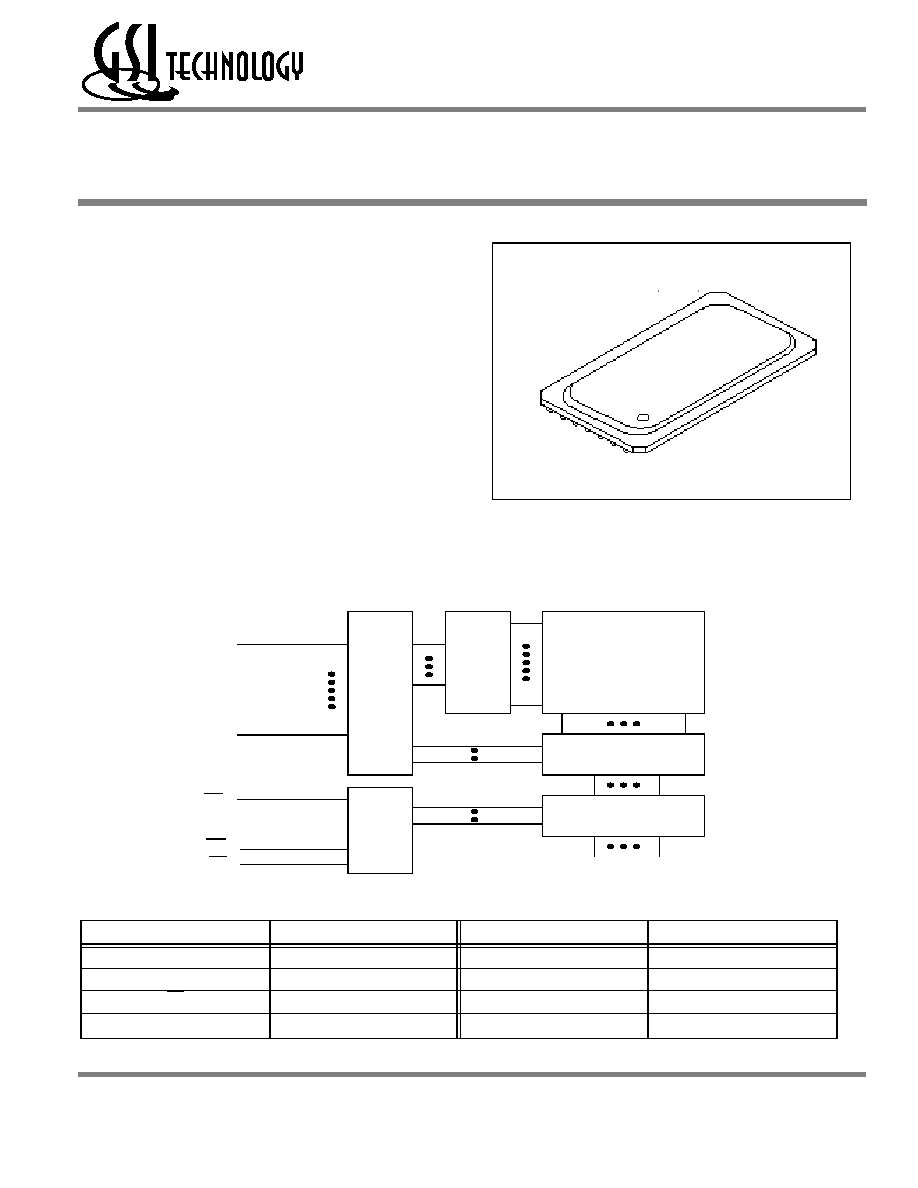
∑ Package
B: 14 mm x 22 mm, 119-bump, 1.27 mm pitch BGA
Description
The GS76024A is a high speed CMOS static RAM organized
as 262,144 words by 24 bits. Static design eliminates the need
for external clocks or timing strobes. Operating on a single 3.3
V power supply and all inputs and outputs are TTL-
compatible. The GS76024A is available in a 119 Bump BGA
package.
119-bump Ball Grid Array Package
Pin Descriptions
Symbol
Description
Symbol
Description
A
0
to A
17
Address input
DQ
1
to DQ
24
Data input/output
WE
Write enable input
OE
Output enable input
CE
Chip enable input
V
DD
+3.3V power supply
V
SS
Ground
CE
WE
OE
Memory Array
Row
Decoder
Column
Decoder
Address
Input
Control
I/O Buffer
A
0
DQ
1
DQ
24
Block Diagram
A
17
Rev: 1.00 2/2003
2/12
© 2003, Giga Semiconductor, Inc.
Specifications cited are subject to change without notice. For latest documentation see http://www.gsitechnology.com.
Preliminary
GS76024AB
119-bump, 1.27 mm Pitch BGA Pad Out
Note: Bumps 3C and 5C are actually NC's but should be wired 3C = V
DD
and 5C = V
SS
to assure compatibility with future
versions.
Top View
1
2
3
4
5
6
7
A
NC
A
3
A
2
A
16
A
1
A
0
NC
B
NC
A
7
A
6
CE
A
5
A
4
NC
C
DQ
13
NC
V
DD
,
NC
A
17
V
SS
,
NC
NC
DQ
12
D
DQ
14
V
DD
V
SS
V
SS
V
SS
V
DD
DQ
11
E
DQ
15
NC
V
DD
V
SS
V
DD
NC
DQ
10
F
DQ
16
V
DD
V
SS
V
SS
V
SS
V
DD
DQ
9
G
DQ
17
NC
V
DD
V
SS
V
DD
NC
DQ
8
H
DQ
18
V
DD
V
SS
V
SS
V
SS
V
DD
DQ
7
J
V
DD
V
SS
V
DD
V
SS
V
DD
V
SS
V
DD
K
DQ
19
V
DD
V
SS
V
SS
V
SS
V
DD
DQ
6
L
DQ
20
NC
V
DD
V
SS
V
DD
NC
DQ
5
M
DQ
21
V
DD
V
SS
V
SS
V
SS
V
DD
DQ
4
N
DQ
22
NC
V
DD
V
SS
V
DD
NC
DQ
3
P
DQ
23
V
DD
V
SS
V
SS
V
SS
V
DD
DQ
2
R
DQ
24
NC
NC
NC
NC
NC
DQ
1
T
NC
A
11
A
10
WE
A
9
A
8
NC
U
NC
A
15
A
14
OE
A
13
A
12
NC

Rev: 1.00 2/2003
3/12
© 2003, Giga Semiconductor, Inc.
Specifications cited are subject to change without notice. For latest documentation see http://www.gsitechnology.com.
Preliminary
GS76024AB
X: "H" or "L"
Note:
Permanent device damage may occur if Absolute Maximum Ratings are exceeded. Functional operation shall be restricted to
Recommended Operating Conditions. Exposure to higher than recommended voltages for extended periods of time could affect
device reliability.
Truth Table
CE
OE
WE
Mode
DQ0 to DQ23
V
DD
Current
H
X
X
Not selected
High Z
ISB1, ISB2
L
L
H
Read
Data Out
I
DD
L
X
L
Write
Data In
L
H
H
Output disable
High Z
Absolute Maximum Ratings
Parameter
Symbol
Rating
Unit
Supply Voltage
V
DD
≠0.5 to +4.6
V
Input Voltage
V
IN
≠0.5 to V
DD
+0.5
(
4.6 V max.)
V
Output Voltage
V
OUT
≠0.5 to V
DD
+0.5
(
4.6 V max.)
V
Allowable BGA power dissipation
PD
1.5
W
Storage temperature
T
STG
≠55 to 150
o
C
Rev: 1.00 2/2003
4/12
© 2003, Giga Semiconductor, Inc.
Specifications cited are subject to change without notice. For latest documentation see http://www.gsitechnology.com.
Preliminary
GS76024AB
Notes:
1. Input overshoot voltage should be less than V
DD
+2 V and not exceed 20 ns.
2. Input undershoot voltage should be greater than ≠2 V and not exceed 20 ns.
Notes:
1. Tested at T
A
= 25∞C, f = 1 MHz
2. These parameters are sampled and are not 100% tested
Recommended Operating Conditions
Parameter
Symbol
Min
Typ
Max
Unit
Supply Voltage for -8/10/12
V
DD
3.0
3.3
3.6
V
Input High Voltage
V
IH
2.0
--
V
DD
+0.3
V
Input Low Voltage
V
IL
≠0.3
--
0.8
V
Ambient Temperature,
Commercial Range
T
Ac
0
--
70
o
C
Ambient Temperature,
Industrial Range
T
Ai
≠40
--
85
o
C
Capacitance
Parameter
Symbol
Test Condition
Max
Unit
Input Capacitance
C
IN
V
IN
= 0 V
10
pF
I/O Capacitance
C
OUT
V
OUT
= 0 V
7
pF
DC I/O Pin Characteristics
Parameter
Symbol
Test Conditions
Min
Max
Input Leakage Current
I
IL
V
IN
= 0 to V
DD
≠2 uA
2 uA
Output Leakage Current
I
OL
Output High Z, V
OUT
= 0
to V
DD
≠1 uA
1 uA
Output High Voltage
V
OH
I
OH
= ≠4 mA
2.4
--
Output Low Voltage
V
OL
I
OL
= +4 mA
--
0.4 V
Rev: 1.00 2/2003
5/12
© 2003, Giga Semiconductor, Inc.
Specifications cited are subject to change without notice. For latest documentation see http://www.gsitechnology.com.
Preliminary
GS76024AB
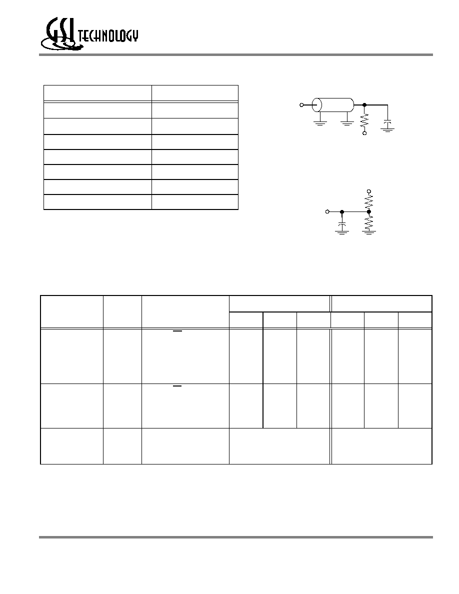
AC Test Conditions
Power Supply Currents
Parameter
Symbol
Test Conditions
0 to 70∞C
≠40 to 85∞C
8 ns
10 ns
12 ns
8 ns
10 ns
12 ns
Operating
Supply
Current
I
DD
CE
V
IL
All other inputs
V
IH
or
V
IL
Min. cycle time
I
OUT
= 0 mA
260 mA
210 mA
180 mA
280 mA
230 mA
200 mA
Standby
Current
I
SB1
CE
V
IH
All other inputs
V
IH
or
V
IL
Min. cycle time
60 mA
50 mA
50 mA
80 mA
70 mA
70 mA
Standby
Current
I
SB2
CE
V
DD
- 0.2V
All other inputs
V
DD
- 0.2V or
0.2V
20 mA
40 mA
DQ
VT = 1.4 V
50
30pF
1
DQ
3.3 V
Output Load 1
Output Load 2
589
434
5pF
1
Notes:
1. Includes scope and jig capacitance.
2. Test conditions as specified with output loading as shown in
Fig. 1 unless otherwise noted
3. Output load 2 for t
LZ
, t
HZ
, t
OLZ
and t
OHZ
.
Parameter
Conditions
Input high level
V
IH
= 2.4 V
Input low level
V
IL
= 0.4 V
Input rise time
tr = 1 V/ns
Input fall time
tf = 1 V/ns
Input reference level
1.4 V
Output reference level
1.4 V
Output load
Fig. 1& 2
Rev: 1.00 2/2003
6/12
© 2003, Giga Semiconductor, Inc.
Specifications cited are subject to change without notice. For latest documentation see http://www.gsitechnology.com.
Preliminary
GS76024AB
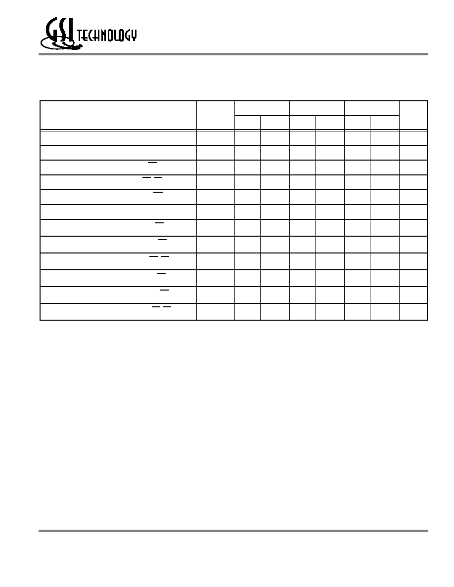
AC Characteristics
* These parameters are sampled and are not 100% tested
Read Cycle
Parameter
Symbol
-8
-10
-12
Unit
Min
Max
Min
Max
Min
Max
Read cycle time
t
RC
8
--
10
--
12
--
ns
Address access time
t
AA
--
8
--
10
--
12
ns
Chip enable access time (CE)
t
AC
--
8
--
10
--
12
ns
Byte enable access time (UB, LB)
t
AB
--
3.5
--
4
--
5
ns
Output enable to output valid (OE)
t
OE
--
3.5
--
4
--
5
ns
Output hold from address change
t
OH
3
--
3
--
3
--
ns
Chip enable to output in low Z (CE)
t
LZ
*
3
--
3
--
3
--
ns
Output enable to output in low Z (OE)
t
OLZ
*
0
--
0
--
0
--
ns
Byte enable to output in low Z (UB, LB)
t
BLZ
*
0
--
0
--
0
--
ns
Chip disable to output in High Z (CE)
t
HZ
*
--
4
--
5
--
6
ns
Output disable to output in High Z (OE)
t
OHZ
*
--
3.5
--
4
--
5
ns
Byte disable to output in High Z (UB, LB)
t
BHZ
*
--
3.5
--
4
--
5
ns
Rev: 1.00 2/2003
7/12
© 2003, Giga Semiconductor, Inc.
Specifications cited are subject to change without notice. For latest documentation see http://www.gsitechnology.com.
Preliminary
GS76024AB
Read Cycle 1: CE = OE = V
IL
, WE = V
IH
Read Cycle 2: WE = V
IH
t
AA
t
OH
t
RC
Address
Data Out
Previous Data
Data valid
t
AA
t
RC
Address
t
AC
t
LZ
t
OE
t
OLZ
CE
OE
Data Out
t
HZ
t
OHZ
Data valid
High impedance
Rev: 1.00 2/2003
8/12
© 2003, Giga Semiconductor, Inc.
Specifications cited are subject to change without notice. For latest documentation see http://www.gsitechnology.com.
Preliminary
GS76024AB
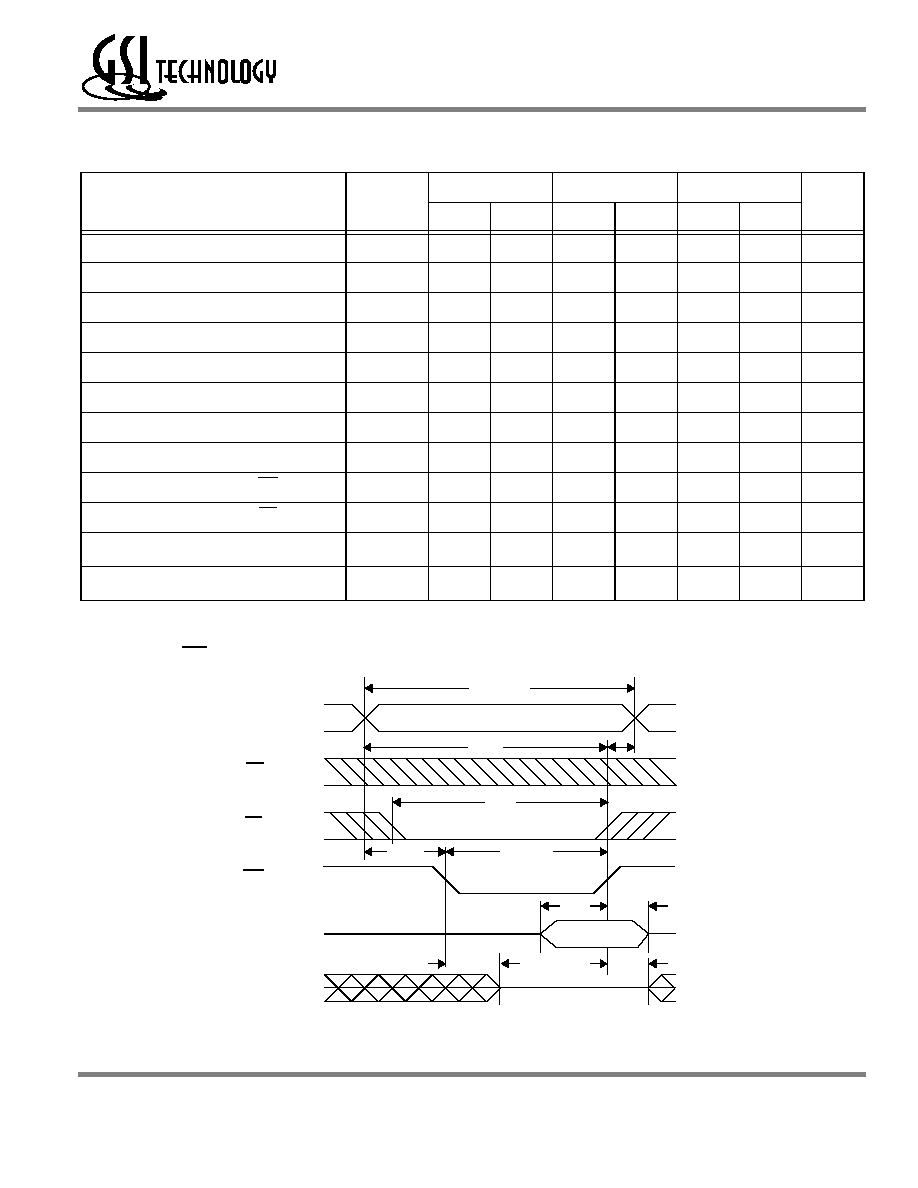
* These parameters are sampled and are not 100% tested
Write Cycle 1: WE control
Write Cycle
Parameter
Symbol
-8
-10
-12
Unit
Min
Max
Min
Max
Min
Max
Write cycle time
tWC
8
--
10
--
12
--
ns
Address valid to end of write
tAW
5.5
--
7
--
8
--
ns
Chip enable to end of write
tCW
5.5
--
7
--
8
--
ns
Byte enable to end of write
tBW
5.5
--
7
--
8
--
ns
Data set up time
tDW
4
--
4.5
--
6
--
ns
Data hold time
tDH
0
--
0
--
0
--
ns
Write pulse width
tWP
5.5
--
7
--
8
--
ns
Address set up time
tAS
0
--
0
--
0
--
ns
Write recovery time (WE)
tWR
0
--
0
--
0
--
ns
Write recovery time (CE)
tWR1
0
--
0
--
0
--
ns
Output Low Z from end of write
tWLZ
*
3
--
3
--
3
--
ns
Write to output in High Z
tWHZ
*
--
3.5
--
4
--
5
ns
t
WC
Address
CE
WE
Data In
OE
Data Out
t
AW
t
CW
t
AS
t
WP
t
WR
t
DW
t
DH
t
WLZ
t
WHZ
Data valid
High impedance
Rev: 1.00 2/2003
9/12
© 2003, Giga Semiconductor, Inc.
Specifications cited are subject to change without notice. For latest documentation see http://www.gsitechnology.com.
Preliminary
GS76024AB
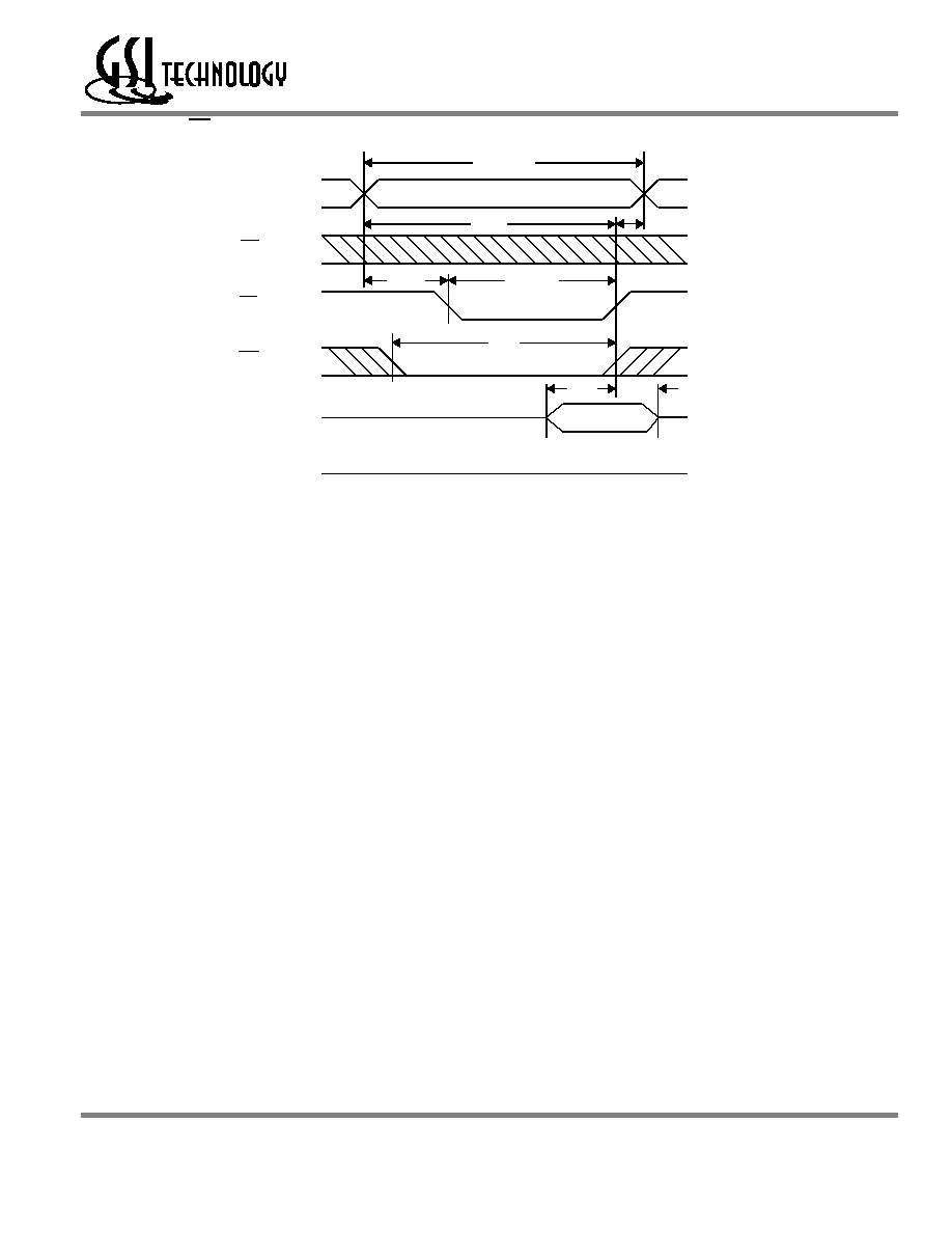
Write Cycle 2: CE control
t
WC
Address
CE
WE
Data In
OE
Data Out
t
AW
t
WP
t
AS
t
CW
t
WR1
t
DW
t
DH
Data valid
High impedance

Rev: 1.00 2/2003
10/12
© 2003, Giga Semiconductor, Inc.
Specifications cited are subject to change without notice. For latest documentation see http://www.gsitechnology.com.
Preliminary
GS76024AB
Package Dimensions--119-bump PBGA
BPR 1999.05.18
N
P
A
B
Pin 1
Corner
K
E
F
CT
A
B
C
D
E
F
G
H
J
K
L
M
N
P
R
T
U
G
S
D
1
2
3
4
5
6
7
Package Admissions - 119 Pin PBGA
Unit: mm
Symbol
Description
Min. Nom. Max
A
Width
13.8
14.0
14.2
B
Length
21.8
22.0
22.2
C
Package Height (including ball)
-
2.40
D
Ball Size
0.60
0.75
0.90
E
Ball Height
0.50
0.60
0.70
F
Package Height (excluding balls)
1.46
1.70
G
Width between Balls
1.27
K
Package Height above board
0.80
0.90
1.00
N
Cut-out Package Width
12.00
P
Foot Length
19.50
R
Width of package between balls
7.62
S
Length of package between balls
20.32
T
Variance of Ball Height
0.15
Bottom View
R
Top View
Side View

Rev: 1.00 2/2003
11/12
© 2003, Giga Semiconductor, Inc.
Specifications cited are subject to change without notice. For latest documentation see http://www.gsitechnology.com.
Preliminary
GS76024AB
Ordering Information
Part Number
Package
Access Time
Temp. Range
Status
GS76024AB-8
119 Bump BGA
8 ns
Commercial
GS76024AB-10
119 Bump BGA
10 ns
Commercial
GS76024AB-12
119 Bump BGA
12 ns
Commercial
GS76024AB-8I
119 Bump BGA
8 ns
Industrial
GS76024AB-10I
119 Bump BGA
10 ns
Industrial
GS76024AB-12I
119 Bump BGA
12 ns
Industrial
* Customers requiring Tape and Reel should add the character "T" to the end of the part number. For example: GS76024AB-12T
Rev: 1.00 2/2003
12/12
© 2003, Giga Semiconductor, Inc.
Specifications cited are subject to change without notice. For latest documentation see http://www.gsitechnology.com.
Preliminary
GS76024AB
Revision History
Rev. Code: Old;
New
Types of Changes
Format or Content
Page/Revisions/Reason
GS76024A_r1
∑ Creation of new datasheet