 | –≠–ª–µ–∫—Ç—Ä–æ–Ω–Ω—ã–π –∫–æ–º–ø–æ–Ω–µ–Ω—Ç: GS815018 | –°–∫–∞—á–∞—Ç—å:  PDF PDF  ZIP ZIP |

Product Preview
GS815018/36AB-357/333/300/250
1M x 18, 512K x 36
18Mb Register-Register Late Write SRAM
250 MHz≠357 MHz
2.5 V V
DD
HSTL I/O
119-Bump BGA
Commercial Temp
Industrial Temp
Rev: 1.05 10/2005
1/25
© 2003, GSI Technology
Specifications cited are subject to change without notice. For latest documentation see http://www.gsitechnology.com.
Features
∑ Register-Register Late Write mode, Pipelined Read mode
∑ 2.5 V +200/≠200 mV core power supply
∑ 1.5 V or 1.8 V HSTL Interface
∑ ZQ controlled programmable output drivers
∑ Dual Cycle Deselect
∑ Fully coherent read and write pipelines
∑ Byte write operation (9-bit bytes)
∑ Differential HSTL clock inputs, K and K
∑ Asynchronous output enable
∑ Sleep mode via ZZ
∑ IEEE 1149.1 JTAG-compliant Serial Boundary Scan
∑ JEDEC-standard 119-bump BGA package
∑ Pb-Free 119-bump BGA package available
Family Overview
GS815018/36A are 18,874,368-bit (18Mb) high performance
SRAMs. This family of wide, low voltage HSTL I/O SRAMs
is designed to operate at the speeds needed to implement
economical high performance cache systems.
Functional Description
Because GS815018/36A are synchronous devices, address data
inputs and read/write control inputs are captured on the rising
edge of the input clock. Write cycles are internally self-timed
and initiated by the rising edge of the clock input. This feature
eliminates complex off-chip write pulse generation required by
asynchronous SRAMs and simplifies input signal timing.
GS815018/36A support pipelined reads utilizing a rising-edge-
triggered output register. They also utilize a Dual Cycle
Deselect (DCD) output deselect protocol.
GS815018/36A are implemented with high performance
technology and are packaged in a 119-bump BGA.
Mode Control
There are two mode control select pins (M1 and M2), which
allow the user to set the correct read protocol for the design.
The GS815018/36A support single clock Pipeline mode, which
directly affects the two mode control select pins. In order for
the part to fuction correctly, and as specified, M1 must be tied
to VSS and M2 must be tied to V
DD
or V
DDQ
. This must be set
at power-up and should not be changed during operation.
Sleep Mode
Low power (Sleep mode) is attained through the assertion (High)
of the ZZ signal, or by stopping the clock (CK). Memory data is
retained during Sleep mode.
Parameter Synopsis
-357
-333
-300
-250
Unit
Pipeline
Cycle
tKHQV
2.8
1.4
3.0
1.5
3.3
1.6
4.0
2.0
ns
ns
Curr (x18)
Curr (x36)
600
650
550
600
500
550
450
500
mA
mA
1
2
3
4
5
6
7
A
V
DDQ
A
A
NC
A
A
V
DDQ
B
NC
A
A
NC
A
A
NC
C
NC
A
A
V
DD
A
A
NC
D
DQ
C
DQ
C
V
SS
ZQ
V
SS
DQ
B
DQ
B
E
DQ
C
DQ
C
V
SS
SS
V
SS
DQ
B
DQ
B
F
V
DDQ
DQ
C
V
SS
G
V
SS
DQ
B
V
DDQ
G
DQ
C
DQ
C
B
C
NC
B
B
DQ
B
DQ
B
H
DQ
C
DQ
C
V
SS
NC
V
SS
DQ
B
DQ
B
J
V
DDQ
V
DD
V
REF
V
DD
V
REF
V
DD
V
DDQ
K
DQ
D
DQ
D
V
SS
CK
V
SS
DQ
A
DQ
A
L
DQ
D
DQ
D
B
D
CK
B
A
DQ
A
DQ
A
M
V
DDQ
DQ
D
V
SS
SW
V
SS
DQ
A
V
DDQ
N
DQ
D
DQ
D
V
SS
A
V
SS
DQ
A
DQ
A
P
DQ
D
DQ
D
V
SS
A
V
SS
DQ
A
DQ
A
R
NC
A
M1
V
DD
M2
A
NC
T
NC
NC
A
A
A
NC
ZZ
U
V
DDQ
TMS
TDI
TCK
TDO
NC
V
DDQ
GS815018/36AB-357/333/300/250
Product Preview
Specifications cited are subject to change without notice. For latest documentation see http://www.gsitechnology.com.
Rev: 1.05 10/2005
2/25
© 2003, GSI Technology
GS815036 Pinout--119-Bump BGA--Top View (Package B)

1
2
3
4
5
6
7
A
V
DDQ
A
A
NC
A
A
V
DDQ
B
NC
A
A
NC
A
A
NC
C
NC
A
A
V
DD
A
A
NC
D
DQ
B
NC
V
SS
ZQ
V
SS
DQ
A
NC
E
NC
DQ
B
V
SS
SS
V
SS
NC
DQ
A
F
V
DDQ
NC
V
SS
G
V
SS
DQ
A
V
DDQ
G
NC
DQ
B
B
B
NC
NC
NC
DQ
A
H
DQ
B
NC
V
SS
NC
V
SS
DQ
A
NC
J
V
DDQ
V
DD
V
REF
V
DD
V
REF
V
DD
V
DDQ
K
NC
DQ
B
V
SS
CK
V
SS
NC
DQ
A
L
DQ
B
NC
NC
CK
B
A
DQ
A
NC
M
V
DDQ
DQ
B
V
SS
SW
V
SS
NC
V
DDQ
N
DQ
B
NC
V
SS
A
V
SS
DQ
A
NC
P
NC
DQ
B
V
SS
A
V
SS
NC
DQ
A
R
NC
A
M1
V
DD
M2
A
NC
T
NC
A
A
NC
A
A
ZZ
U
V
DDQ
TMS
TDI
TCK
TDO
NC
V
DDQ
GS815018/36AB-357/333/300/250
Product Preview
Specifications cited are subject to change without notice. For latest documentation see http://www.gsitechnology.com.
Rev: 1.05 10/2005
3/25
© 2003, GSI Technology
GS815018 Pinout--119-Bump BGA--Top View (Package B)
GS815018/36AB-357/333/300/250
Product Preview
Specifications cited are subject to change without notice. For latest documentation see http://www.gsitechnology.com.
Rev: 1.05 10/2005
4/25
© 2003, GSI Technology
GS815018/36 BGA Pin Description
Symbol
Type
Description
A
I
Address Inputs
DQ
A
DQ
B
DQ
C
DQ
D
I/O
Data Input and Output pins
B
A
, B
B
, B
C
, B
D
I
Byte Write Enable for DQ
A
, DQ
B
, DQ
C
, DQ
D
I/Os; active low
NC
--
No Connect
CK
I
Clock Input Signal; active high
CK
I
Clock Input Signal; active low
SW
I
Write Enable; active low
G
I
Output Enable; active low
ZZ
I
Sleep mode control; active high
M1
I
Read Operation Protocol Select--Selects Register-Register read operations; must be tied low in this
device
M2
I
Read Operation Protocol Select--Selects Register-Register read operations; must be tied high in this
device
ZQ
I
FLXDrive-IITM Output Impedance Control
SS
I
Synchronous Select Input
TMS
I
Scan Test Mode Select
TDI
I
Scan Test Data In
TDO
O
Scan Test Data Out
TCK
I
Scan Test Clock
V
REF
I
Input Reference Voltage
V
DD
I
Core power supply
V
SS
I
I/O and Core Ground
V
DDQ
I
Output driver power supply
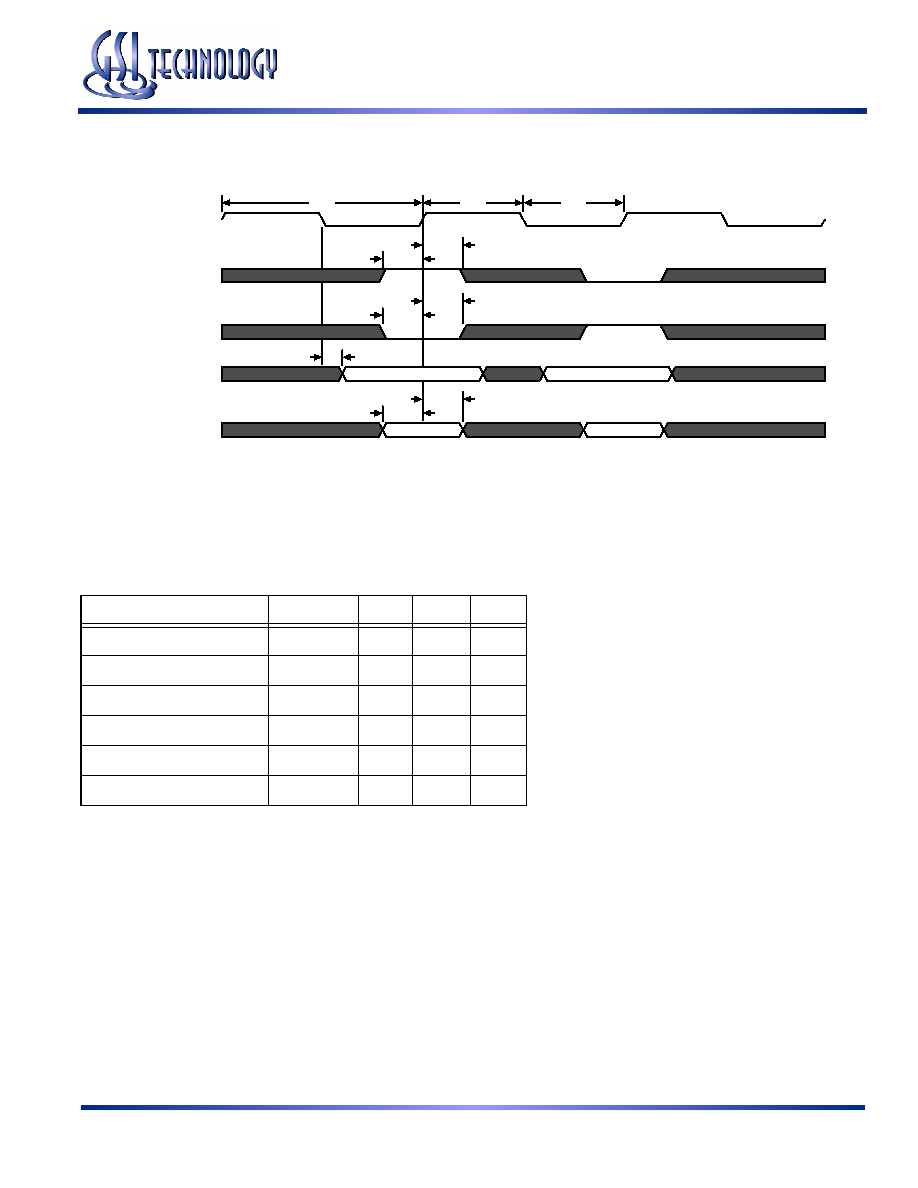
Read Operations
Pipelined Read
A read cycle begins when the RAM captures logic 0 on SS and logic 1 on SW at the rising edge of K (and the falling edge of K).
Address inputs captured on that clock edge are propigated into the RAM, which delivers data to the input of the output registers.
The second rising edge of K fires the output registers and releases read data to the output drivers. If G is held active low, the
drivers drive the data onto the output pins. Read data is sustained on the output pins as long as G is held low or until the next rising
edge of K, at which point the outputs may update to new data or deselect, depending on what control command was registered at
the second rising edge of K.
Dual Cycle Deselect
Chip deselect (SS = logic 1) is pipelined to the same degree as read data. Therefore, a deselect command entered on the rising edge
of K is acted upon in response to the next rising edge of K.

GS815018/36AB-357/333/300/250
Product Preview
Specifications cited are subject to change without notice. For latest documentation see http://www.gsitechnology.com.
Rev: 1.05 10/2005
5/25
© 2003, GSI Technology
Write Operations
Write operations are initiated when the write enable input signal (SW) and chip select (SS) are captured at logic 0 on a rising edge
of the K clock (and falling edge of the K clock).
Late Write
In Late Write mode the RAM requires Data In one rising clock edge later than the edge used to load Address and Control. Late
Write protocol has been employed on SRAMs designed for RISC processor L2 cache applications and in Flow Through mode NBT
SRAMs.
Byte Write Control
The Byte Write Enable inputs (Bx) determine which bytes will be written. Any combination of Byte Write Enable control pins,
including all or none, may be activated. A Write Cycle with no Byte Write inputs active is a write abort cycle. Byte write control
inputs are captured by the same clock edge used to capture SW.
Example of x36 Byte Write Truth Table
Function
SW
Ba
Bb
Bc
Bd
Read
H
X
X
X
X
Write Byte A
L
L
H
H
H
Write Byte B
L
H
L
H
H
Write Byte C
L
H
H
L
H
Write Byte D
L
H
H
H
L
Write all Bytes
L
L
L
L
L
Write Abort
L
H
H
H
H

Register-Register Late Write, Pipelined Read Truth Table
CK
ZZ
SS
SW
Bx
G
Current Operation
DQ
(t
n
)
DQ
(t
n+1
)
X
1
X
X
X
X
Sleep (Power Down) mode
Hi-Z
Hi-Z
0
1
X
X
X
Deselect
***
Hi-Z
0
0
1
X
1
Read
Hi-Z/
Hi-Z
0
0
1
X
0
Read
***
Q(t
n
)
0
0
0
0
X
Write All Bytes
***
D(t
n
)
0
0
0
X
X
Write Bytes with Bx = 0
***
D(t
n
)
0
0
0
1
X
Write (Abort)
***
Hi-Z
Notes:
1. If one or more Bx = 0, then B = "T" else B = "F".
2. "1" = input "high"; "0" = input "low"; "X" = input "don't care".
3. "***" indicates that the DQ input requirement/output state and CQ output state are determined by the previous operation.
4. DQs are tristated in response to Bank Deselect, Deselect, and Write commands, one full cycle after the command is sampled.
5. CQs are tristated in response to Bank Deselect commands only, one full cycle after the command is sampled.
6. Up to three (3) Continue operations may be initiated after a Read or Write operation is initiated to burst transfer up to four (4) distinct pieces
of data per single external address input. If a fourth (4th) Continue operation is initiated, the internal address wraps back to the initial exter-
nal (base) address.
GS815018/36AB-357/333/300/250
Product Preview
Specifications cited are subject to change without notice. For latest documentation see http://www.gsitechnology.com.
Rev: 1.05 10/2005
6/25
© 2003, GSI Technology

Absolute Maximum Ratings
(All voltages reference to V
SS
)
Symbol
Description
Value
Unit
V
DD
Voltage on V
DD
Pins
≠0.5 to 3.6
V
V
DDQ
Voltage in V
DDQ
Pins
≠0.5 to V
DD
V
V
I/O
Voltage on I/O Pins
≠0.5 to V
DDQ
+ 0.5 (
3.6 V max.)
V
V
IN
Voltage on Other Input Pins
≠0.5 to V
DDQ
+ 0.5 (
3.6 V max.)
V
I
IN
Input Current on Any Pin
+/≠20
mA dc
I
OUT
Output Current on Any I/O Pin
+/≠20
mA dc
T
J
Maximum Junction Temperature
125
o
C
T
STG
Storage Temperature
≠55 to 125
∫
C
GS815018/36AB-357/333/300/250
Product Preview
Specifications cited are subject to change without notice. For latest documentation see http://www.gsitechnology.com.
Rev: 1.05 10/2005
7/25
© 2003, GSI Technology
Note:
Permanent damage to the device may occur if the Absolute Maximum Ratings are exceeded. Operation should be restricted to Recommended
Operating Conditions. Exposure to conditions exceeding the Recommended Operating Conditions, for an extended period of time, may affect
reliability of this component.
Recommended Operating Conditions
Power Supplies
Parameter
Symbol
Min.
Typ.
Max.
Unit
Notes
Supply Voltage
V
DD
2.3
2.5
2.7
V
Ambient Temperature
(Commercial Range Versions)
T
A
0
25
70
∞C
Ambient Temperature
(Industrial Range Versions)
T
A
≠40
25
85
∞C
1
Note:
The part number of Industrial Temperature Range versions end the character "I". Unless otherwise noted, all performance specifications quoted
are evaluated for worst case in the temperature range marked on the device.

Common Mode and Differential Voltage
-1.8
-1.6
-1.4
-1.2
-1
-0.8
-0.6
-0.4
-0.2
0
0.2
0.4
0.6
0.8
1
1.2
1.4
1.6
1.8
0
20
40
60
80
100
120
Time
Vol
t
s
K
K#
VCM
VDIF
VCM
GS815018/36AB-357/333/300/250
Product Preview
Specifications cited are subject to change without notice. For latest documentation see http://www.gsitechnology.com.
Rev: 1.05 10/2005
8/25
© 2003, GSI Technology
20% tKC
V
SS
≠ 1.0 V
50%
V
SS
V
IH
Undershoot Measurement and Timing
Overshoot Measurement and Timing
20% tKC
V
DD
+ 1.0 V
50%
V
DD
V
IL

Capacitance
o
C, f = 1 MH
Z
, V
DD
Parameter
Symbol
Test conditions
Max.
Unit
Input Capacitance
C
IN
V
IN
= 0 V
4
pF
Output Capacitance
C
OUT
V
OUT
= 0 V
5
pF
Output Capacitance (Clock)
C
IN(CK)
V
IN
= 0 V
5
pF
GS815018/36AB-357/333/300/250
Product Preview
Specifications cited are subject to change without notice. For latest documentation see http://www.gsitechnology.com.
Rev: 1.05 10/2005
9/25
© 2003, GSI Technology
Note:
This parameter is sample tested.
AC Test Conditions
Parameter
Conditions
Input high level
1.25 V
Input low level
0.25 V
Input rise/fall time (10% to 90%)
0.5 ns/0.5 ns
Input reference level
V
DDQ
/2
Clock input reference level
Differential cross point
Output reference level
V
DDQ
/2
Clock (V
DIF
)
0.75 V
Clock (V
CM
)
0.75 V
V
DDQ
1.5 V
RQ
250
DQ
V
DDQ
/2
50
50
50
50
V
DDQ
/2
V
DDQ
/2
25
5pF
5pF
Device Under Test
V
DDQ
= 1.5 V
ZQ
RQ = 250
AC Test Load Diagram
(T
A
= 25
= 1.8 V)

Input and Output Leakage Characteristics
Parameter
Symbol
Test Conditions
Min.
Max
Notes
Input Leakage Current
(except mode pins)
I
IL
V
IN
= 0 to V
DDQ
≠1 uA
1 uA
--
ZQ, MCH, MCL, EP2, EP3
Pin Input Current
I
INM
V
IN
= 0 to V
DDQ
≠100 uA
1 uA
--
Output Leakage Current
I
OL
Output Disable,
V
OUT
= 0 to V
DDQ
≠1 uA
1 uA
--
Operating Currents
Parameter
Symbol
-357
-333
-300
-250
Test Conditions
0∞C
to
70∞C
≠40∞C
to
+85∞C
0∞C
to
70∞C
≠40∞C
to
+85∞C
0∞C
to
70∞C
≠40∞C
to
+85∞C
0∞C
to
70∞C
≠40∞C
to
+85∞C
Operating
Current
x36
I
DD
650 mA
660 mA
600 mA
610 mA
550 mA
560 mA
500 mA
510 mA
SS
V
IL
Max.
tKHKH
tKHKH Min.
All other inputs
V
IL
V
IN
V
IH
x18
I
DD
600 mA
610 mA
550 mA
560 mA
500 mA
510 mA
450 mA
460 mA
HSTL
Deselect
Current
I
DD3
150 mA
160 mA
150 mA
160 mA
150 mA
160 mA
150 mA
160 mA
Device Deselected
All inputs
V
SS
+ 0.10 V
V
IN
V
DD
≠ 0.10 V
GS815018/36AB-357/333/300/250
Product Preview
Specifications cited are subject to change without notice. For latest documentation see http://www.gsitechnology.com.
Rev: 1.05 10/2005
10/25
© 2003, GSI Technology

AC Electrical Characteristics
Parameter
Symbol
-357
-333
-300
-250
Unit
Notes
Min
Max
Min
Max
Min
Max
Min
Max
Clock Cycle Time
tKHKH
2.8
--
3.0
--
3.3
--
4.0
--
ns
--
Clock High Time
tKHKL
1.1
--
1.2
--
1.3
--
1.5
--
ns
--
Clock Low Time
tKLKH
1.1
--
1.2
--
1.3
--
1.5
--
ns
--
Clock High to Output Low-Z
tKHQX1
0.5
--
0.5
--
0.5
--
0.5
--
ns
1
Clock High to Output Valid
tKHQV
--
1.4
--
1.5
1.6
--
2.0
ns
--
Clock High to Output Invalid
tKHQX
0.5
--
0.5
--
0.5
--
0.5
--
ns
--
Clock High to Output High-Z
tKHQZ
--
1.4
--
1.5
1.6
--
2.0
ns
1
Address Valid to Clock High
tAVKH
0.5
--
0.6
--
0.7
--
0.8
--
ns
--
Clock High to Address Don't Care
tKHAX
0.4
--
0.4
--
0.4
--
0.5
--
ns
--
Enable Valid to Clock High
tEVKH
0.5
--
0.6
--
0.7
--
0.8
--
ns
--
Clock High to Enable Don't Care
tKHEX
0.4
--
0.4
--
0.4
--
0.5
--
ns
--
Write Valid to Clock High
tWVKH
0.5
--
0.6
--
0.7
--
0.8
--
ns
--
Clock High to Write Don't Care
tKHWX
0.4
--
0.4
--
0.4
--
0.5
--
ns
--
Byte Write Valid to Clock High
tBVKH
0.5
--
0.6
--
0.7
--
0.8
--
ns
--
Clock High to Byte Write Don't Care
tKHBX
0.4
--
0.4
--
0.4
--
0.5
--
ns
--
Data In Valid to Clock High
tDVKH
0.5
--
0.5
--
0.5
--
0.5
--
ns
--
Clock High to Data In Don't Care
tKHDX
0.4
--
0.4
--
0.4
--
0.5
--
ns
--
Output Enable Low to Output Data Valid
tGLQV
--
1.4
--
1.5
1.6
--
2.0
ns
--
Output Enable Low to Output Data Low-Z
tGLQX
0
--
0
--
0
--
0
--
ns
--
Output Enable High to Output Data High-Z
tGHQZ
--
1.4
--
1.5
1.6
--
2.0
ns
--
Sleep Mode Enable Time
tZZE
--
15
--
15
--
15
--
15
ns
--
Sleep Mode Recovery Time
tZZR
20
--
20
--
20
--
20
--
ns
--
Notes:
1. Measured at 100 mV from steady state. Not 100% tested.
2. Guaranteed by design. Not 100% tested.
GS815018/36AB-357/333/300/250
Product Preview
Specifications cited are subject to change without notice. For latest documentation see http://www.gsitechnology.com.
Rev: 1.05 10/2005
11/25
© 2003, GSI Technology

GS815018/36AB-357/333/300/250
Product Preview
Specifications cited are subject to change without notice. For latest documentation see http://www.gsitechnology.com.
Rev: 1.05 10/2005
12/25
© 2003, GSI Technology
G Controlled Read-Write
Read A1
Read A2
Read A0
Write A3
Write A4
Read A5
Read A4
Read A6
Read A7
KHQV
KHQX1
KHDX
DVKH
GHQZ
KHQX
GLQV
GLQX
tKHWX
tWVKH
tKHWX
tWVKH
tKHAX
tAVKH
KLKH
KLKH
KHKL
KHKL
KHKH
KHKH
A1
A2
A3
A4
A5
A4
A6
A7
Q1
Q2
D3
D4
Q5
Q4
A0
Q6
K
A
G
SW
BWx
DQn
Note:
K is not shown; assumes K tied to V
REF
or out of phase with K
SS Controlled Read-Write
Read A1
Read A2
Deselect
Write A3
Write A4
Read A5
Read A4
Read A6
Read A7
KHQX
tKHDX
tDVKH
KHQZ
KHQV
KHQX1
tKHBX
tBVKH
tKHWX
tWVKH
tKHEX
tEVKH
tKHAX
tAVKH
KLKH
KLKH
KHKL
KHKL
KHKH
KHKH
A1
A2
A3
A4
A5
A4
A6
A7
Q1
Q2
D3
D4
Q5
Q4
K
A
SS
SW
BWx
DQn
Note:
K is not shown; assumes K tied to V
REF
or out of phase with K
GS815018/36AB-357/333/300/250
Product Preview
Specifications cited are subject to change without notice. For latest documentation see http://www.gsitechnology.com.
Rev: 1.05 10/2005
13/25
© 2003, GSI Technology
ZZ Timing
Read A1
Read A2
Deselect
Clock is a Don't care during Sleep ModeRead A1
Read A2
Read A3
KHQX
KHQV
ZZE
KHQX1
ZZR
tKHWX
tWVKH
tKHEX
tEVKH
tKHAX
tAVKH
KLKH
KLKH
KHKL
KHKL
KHKH
KHKH
A1
A2
A1
A2
A3
Q1
Q2
Q1
Begin ISB
K
A
SS
SW
SWx
ZZ
DQn
Note:
K is not shown; assumes K tied to V
REF
or out of phase with K
JTAG Port Operation
Overview
The JTAG Port on this RAM operates in a manner that is compliant with IEEE Standard 1149.1-1990, a serial boundary scan
interface standard (commonly referred to as JTAG). The JTAG Port input interface levels scale with V
DD
. The JTAG output
drivers are powered by V
DDQ
.
Disabling the JTAG Port
It is possible to use this device without utilizing the JTAG port. The port is reset at power-up and will remain inactive unless
clocked. TCK, TDI, and TMS are designed with internal pull-up circuits.To assure normal operation of the RAM with the JTAG
Port unused, TCK, TDI, and TMS may be left floating or tied to either V
DD
or V
SS
. TDO should be left unconnected.

JTAG Pin Descriptions
Pin
Pin Name
I/O
Description
TCK
Test Clock
In
Clocks all TAP events. All inputs are captured on the rising edge of TCK and all outputs propagate
from the falling edge of TCK.
TMS
Test Mode Select
In
The TMS input is sampled on the rising edge of TCK. This is the command input for the TAP
controller state machine. An undriven TMS input will produce the same result as a logic one input
level.
TDI
Test Data In
In
The TDI input is sampled on the rising edge of TCK. This is the input side of the serial registers
placed between TDI and TDO. The register placed between TDI and TDO is determined by the
state of the TAP Controller state machine and the instruction that is currently loaded in the TAP
Instruction Register (refer to the TAP Controller State Diagram). An undriven TDI pin will produce
the same result as a logic one input level.
TDO
Test Data Out
Out
Output that is active depending on the state of the TAP state machine. Output changes in
response to the falling edge of TCK. This is the output side of the serial registers placed between
TDI and TDO.
Note:
This device does not have a TRST (TAP Reset) pin. TRST is optional in IEEE 1149.1. The Test-Logic-Reset state is entered while TMS is
held high for five rising edges of TCK. The TAP Controller is also reset automaticly at power-up.
GS815018/36AB-357/333/300/250
Product Preview
Specifications cited are subject to change without notice. For latest documentation see http://www.gsitechnology.com.
Rev: 1.05 10/2005
14/25
© 2003, GSI Technology
JTAG Port Registers
Overview
The various JTAG registers, refered to as Test Access Port orTAP Registers, are selected (one at a time) via the sequences of 1s
and 0s applied to TMS as TCK is strobed. Each of the TAP Registers is a serial shift register that captures serial input data on the
rising edge of TCK and pushes serial data out on the next falling edge of TCK. When a register is selected, it is placed between the
TDI and TDO pins.
Instruction Register
The Instruction Register holds the instructions that are executed by the TAP controller when it is moved into the Run, Test/Idle, or
the various data register states. Instructions are 3 bits long. The Instruction Register can be loaded when it is placed between the
TDI and TDO pins. The Instruction Register is automatically preloaded with the IDCODE instruction at power-up or whenever the
controller is placed in Test-Logic-Reset state.
Bypass Register
The Bypass Register is a single bit register that can be placed between TDI and TDO. It allows serial test data to be passed through
the RAM's JTAG Port to another device in the scan chain with as little delay as possible.
Boundary Scan Register
The Boundary Scan Register is a collection of flip flops that can be preset by the logic level found on the RAM's input or I/O pins.
The flip flops are then daisy chained together so the levels found can be shifted serially out of the JTAG Port's TDO pin. The
Boundary Scan Register also includes a number of place holder flip flops (always set to a logic 1). The relationship between the
device pins and the bits in the Boundary Scan Register is described in the Scan Order Table following. The Boundary Scan
Register, under the control of the TAP Controller, is loaded with the contents of the RAMs I/O ring when the controller is in
Capture-DR state and then is placed between the TDI and TDO pins when the controller is moved to Shift-DR state. SAMPLE-Z,
SAMPLE/PRELOAD and EXTEST instructions can be used to activate the Boundary Scan Register.

Instruction Register
ID Code Register
Boundary Scan Register
0
1
2
0
∑
∑ ∑ ∑
31 30 29
1
2
0
Bypass Register
TDI
TDO
TMS
TCK
Test Access Port (TAP) Controller
108
∑
1
0
∑
∑
∑
∑
∑
∑
∑
∑
∑
Control Signals
∑
GS815018/36AB-357/333/300/250
Product Preview
Specifications cited are subject to change without notice. For latest documentation see http://www.gsitechnology.com.
Rev: 1.05 10/2005
15/25
© 2003, GSI Technology
JTAG TAP Block Diagram
Identification (ID) Register
The ID Register is a 32-bit register that is loaded with a device and vendor specific 32-bit code when the controller is put in
Capture-DR state with the IDCODE command loaded in the Instruction Register. The code is loaded from a 32-bit on-chip ROM.
It describes various attributes of the RAM as indicated below. The register is then placed between the TDI and TDO pins when the
controller is moved into Shift-DR state. Bit 0 in the register is the LSB and the first to reach TDO when shifting begins.

ID Register Contents
Die
Revision
Code
Not Used
I/O
Configuration
GSI Technology
JEDEC Vendor
ID Code
Presence Register
Bit # 31 30 29 28 27 26 25 24 23 22 21 20 19 18 17 16 15 14 13 12 11 10 9 8 7 6 5 4 3 2 1
0
x36
X X X X
0
0
0
X
1
0
0
1
0
0
0
0
1
0
0
0
0
0 0 1 1 0 1 1 0 0 1
1
x18
X X X X
0
0
0
X
1
0
0
1
0
0
0
0
1
0
1
0
0
0 0 1 1 0 1 1 0 0 1
1
GS815018/36AB-357/333/300/250
Product Preview
Specifications cited are subject to change without notice. For latest documentation see http://www.gsitechnology.com.
Rev: 1.05 10/2005
16/25
© 2003, GSI Technology
Tap Controller Instruction Set
Overview
There are two classes of instructions defined in the Standard 1149.1-1990; the standard (Public) instructions, and device specific
(Private) instructions. Some Public instructions are mandatory for 1149.1 compliance. Optional Public instructions must be
implemented in prescribed ways. The TAP on this device may be used to monitor all input and I/O pads, and can be used to load
address, data or control signals into the RAM or to preload the I/O buffers.
When the TAP controller is placed in Capture-IR state the two least significant bits of the instruction register are loaded with 01.
When the controller is moved to the Shift-IR state the Instruction Register is placed between TDI and TDO. In this state the desired
instruction is serially loaded through the TDI input (while the previous contents are shifted out at TDO). For all instructions, the
TAP executes newly loaded instructions only when the controller is moved to Update-IR state. The TAP instruction set for this
device is listed in the following table.

Select DR
Capture DR
Shift DR
Exit1 DR
Pause DR
Exit2 DR
Update DR
Select IR
Capture IR
Shift IR
Exit1 IR
Pause IR
Exit2 IR
Update IR
Test Logic Reset
Run Test Idle
0
0
1
0
1
1
0
0
1
1
1
0
0
1
1
0
0
0
0
1
1
0
0
1
1
0
0
0
1
1
1
1
GS815018/36AB-357/333/300/250
Product Preview
Specifications cited are subject to change without notice. For latest documentation see http://www.gsitechnology.com.
Rev: 1.05 10/2005
17/25
© 2003, GSI Technology
JTAG Tap Controller State Diagram
Instruction Descriptions
BYPASS
When the BYPASS instruction is loaded in the Instruction Register the Bypass Register is placed between TDI and TDO. This
occurs when the TAP controller is moved to the Shift-DR state. This allows the board level scan path to be shortened to facili-
tate testing of other devices in the scan path.
SAMPLE/PRELOAD
SAMPLE/PRELOAD is a Standard 1149.1 mandatory public instruction. When the SAMPLE / PRELOAD instruction is
loaded in the Instruction Register, moving the TAP controller into the Capture-DR state loads the data in the RAMs input and
I/O buffers into the Boundary Scan Register. Boundary Scan Register locations are not associated with an input or I/O pin, and
are loaded with the default state identified in the Boundary Scan Chain table at the end of this section of the datasheet. Because
the RAM clock is independent from the TAP Clock (TCK) it is possible for the TAP to attempt to capture the I/O ring contents
while the input buffers are in transition (i.e. in a metastable state). Although allowing the TAP to sample metastable inputs will
not harm the device, repeatable results cannot be expected. RAM input signals must be stabilized for long enough to meet the
TAPs input data capture set-up plus hold time (tTS plus tTH). The RAMs clock inputs need not be paused for any other TAP
operation except capturing the I/O ring contents into the Boundary Scan Register. Moving the controller to Shift-DR state then
places the boundary scan register between the TDI and TDO pins.
EXTEST
EXTEST is an IEEE 1149.1 mandatory public instruction. It is to be executed whenever the instruction register is loaded with
all logic 0s. The EXTEST command does not block or override the RAM's input pins; therefore, the RAM's internal state is
still determined by its input pins.

GS815018/36AB-357/333/300/250
Product Preview
Specifications cited are subject to change without notice. For latest documentation see http://www.gsitechnology.com.
Rev: 1.05 10/2005
18/25
© 2003, GSI Technology
Typically, the Boundary Scan Register is loaded with the desired pattern of data with the SAMPLE/PRELOAD command.
Then the EXTEST command is used to output the Boundary Scan Register's contents, in parallel, on the RAM's data output
drivers on the falling edge of TCK when the controller is in the Update-IR state.
Alternately, the Boundary Scan Register may be loaded in parallel using the EXTEST command. When the EXTEST instruc-
tion is selected, the sate of all the RAM's input and I/O pins, as well as the default values at Scan Register locations not asso-
ciated with a pin, are transferred in parallel into the Boundary Scan Register on the rising edge of TCK in the Capture-DR
state, the RAM's output pins drive out the value of the Boundary Scan Register location with which each output pin is associ-
ated.
IDCODE
The IDCODE instruction causes the ID ROM to be loaded into the ID register when the controller is in Capture-DR mode and
places the ID register between the TDI and TDO pins in Shift-DR mode. The IDCODE instruction is the default instruction
loaded in at power up and any time the controller is placed in the Test-Logic-Reset state.
SAMPLE-Z
If the SAMPLE-Z instruction is loaded in the instruction register, all RAM outputs are forced to an inactive drive state (high-
Z) and the Boundary Scan Register is connected between TDI and TDO when the TAP controller is moved to the Shift-DR
state.
RFU
These instructions are Reserved for Future Use. In this device they replicate the BYPASS instruction.

JTAG TAP Instruction Set Summary
Instruction
Code
Description
Notes
EXTEST
000
Places the Boundary Scan Register between TDI and TDO.
1
IDCODE
001
Preloads ID Register and places it between TDI and TDO.
1, 2
SAMPLE-Z
010
Captures I/O ring contents. Places the Boundary Scan Register between TDI and
TDO.
Forces all RAM output drivers to High-Z.
1
RFU
011
Do not use this instruction; Reserved for Future Use.
Replicates BYPASS instruction. Places Bypass Register between TDI and TDO.
1
SAMPLE/
PRELOAD
100
Captures I/O ring contents. Places the Boundary Scan Register between TDI and
TDO.
1
GSI
101
GSI private instruction.
1
RFU
110
Do not use this instruction; Reserved for Future Use.
Replicates BYPASS instruction. Places Bypass Register between TDI and TDO.
1
BYPASS
111
Places Bypass Register between TDI and TDO.
1
Notes:
1. Instruction codes expressed in binary, MSB on left, LSB on right.
2. Default instruction automatically loaded at power-up and in test-logic-reset state.
GS815018/36AB-357/333/300/250
Product Preview
Specifications cited are subject to change without notice. For latest documentation see http://www.gsitechnology.com.
Rev: 1.05 10/2005
19/25
© 2003, GSI Technology
Notes:
1. Include scope and jig capacitance.
2. Test conditions as shown unless otherwise noted.
JTAG Port AC Test Conditions
Parameter
Conditions
Input high level
V
DD
≠ 0.2 V
Input low level
0.2 V
Input slew rate
1 V/ns
Input reference level
V
DDQ
/2
Output reference level
V
DDQ
/2
DQ
V
DDQ
/2
50
30pF
*
JTAG Port AC Test Load
* Distributed Test Jig Capacitance
JTAG Port Recommended Operating Conditions and DC Characteristics
Parameter
Symbol
Min.
Max.
Unit Notes
3.3 V Test Port Input High Voltage
V
IHJ3
2.0
V
DD3
+0.3
V
1
3.3 V Test Port Input Low Voltage
V
ILJ3
≠0.3
0.8
V
1
2.5 V Test Port Input High Voltage
V
IHJ2
0.6 * V
DDQ2
V
DDQ2
+0.3
V
1
2.5 V Test Port Input Low Voltage
V
ILJ2
≠0.3
0.3 * V
DDQ2
V
1
TMS, TCK and TDI Input Leakage Current
I
INHJ
≠300
1
uA
2
TMS, TCK and TDI Input Leakage Current
I
INLJ
≠1
100
uA
3
TDO Output Leakage Current
I
OLJ
≠1
1
uA
4
Test Port Output High Voltage
V
OHJ
1.7
--
V
5, 6
Test Port Output Low Voltage
V
OLJ
--
0.4
V
5, 7
Test Port Output CMOS High
V
OHJC
V
DDQ
≠ 100 mV
--
V
5, 8
Test Port Output CMOS Low
V
OLJC
--
100 mV
V
5, 9
Notes:
1. Input Under/overshoot voltage must be ≠1 V > Vi < V
DDn
+1 V not to exceed 3.6 V maximum, with a pulse width not to exceed 20% tTKC.
2. V
ILJ
V
IN
V
DDQ
3. 0 V
V
IN
V
ILJn
4. Output Disable, V
OUT
= 0 to V
DDQ
5. The TDO output driver is served by the V
DDQ
supply.
6. I
OHJ
= ≠4 mA
7. I
OLJ
= + 4 mA
8. I
OHJC
= ≠100 uA
9. I
OLJC
= +100 uA
GS815018/36AB-357/333/300/250
Product Preview
Specifications cited are subject to change without notice. For latest documentation see http://www.gsitechnology.com.
Rev: 1.05 10/2005
20/25
© 2003, GSI Technology
GS815018/36AB-357/333/300/250
Product Preview
Specifications cited are subject to change without notice. For latest documentation see http://www.gsitechnology.com.
Rev: 1.05 10/2005
21/25
© 2003, GSI Technology
JTAG Port Timing Diagram
tTH
tTS
tTKQ
tTH
tTS
tTH
tTS
tTKL
tTKL
tTKH
tTKH
tTKC
tTKC
TCK
TDI
TMS
TDO
Parallel SRAM input
JTAG Port AC Electrical Characteristics
Parameter
Symbol
Min
Max
Unit
TCK Cycle Time
tTKC
50
--
ns
TCK Low to TDO Valid
tTKQ
--
20
ns
TCK High Pulse Width
tTKH
20
--
ns
TCK Low Pulse Width
tTKL
20
--
ns
TDI & TMS Set Up Time
tTS
10
--
ns
TDI & TMS Hold Time
tTH
10
--
ns

GS815018/36AB-357/333/300/250
Product Preview
Specifications cited are subject to change without notice. For latest documentation see http://www.gsitechnology.com.
Rev: 1.05 10/2005
22/25
© 2003, GSI Technology
Package Dimensions--119-Bump FPBGA (Package B, Variation 2
)
A
B
C
D
E
F
G
H
J
K
L
M
N
P
R
T
U
1 2 3 4 5 6 7
7 6 5 4 3 2 1
A1
TOP VIEW
A1
BOTTOM VIEW
1.27
7.62
1.
27
20
.3
2
14±0.10
22±0.10
B
A
0.20(4x)
ÿ0.10
ÿ0.30
C
C A B
S
S
ÿ0.60~0.90 (119x)
C
SEATING PLANE
0.
15
C
0.
50
~0
.70
1.
86.
±0.
13
A
B
C
D
E
F
G
H
J
K
L
M
N
P
R
T
U
S
S

GS815018/36AB-357/333/300/250
Product Preview
Specifications cited are subject to change without notice. For latest documentation see http://www.gsitechnology.com.
Rev: 1.05 10/2005
23/25
© 2003, GSI Technology
Ordering Information
Org
Part Number
Type
I/O
Speed
(MHz)
T
A
1M x 18
GS815018AB-357
Register-Register Late Write SRAM
357 MHz
C
1M x 18
GS815018AB-333
Register-Register Late Write SRAM
333 MHz
C
1M x 18
GS815018AB-300
Register-Register Late Write SRAM
300 MHz
C
1M x 18
GS815018AB-250
Register-Register Late Write SRAM
250 MHz
C
512K x 36
GS815036AB-357
Register-Register Late Write SRAM
357MHz
C
512K x 36
GS815036AB-333
Register-Register Late Write SRAM
333 MHz
C
512K x 36
GS815036AB-300
Register-Register Late Write SRAM
300 MHz
C
512K x 36
GS815036AB-250
Register-Register Late Write SRAM
250 MHz
C
1M x 18
GS815018AB-357I
Register-Register Late Write SRAM
357 MHz
I
1M x 18
GS815018AB-333I
Register-Register Late Write SRAM
333 MHz
I
1M x 18
GS815018AB-300I
Register-Register Late Write SRAM
300 MHz
I
1M x 18
GS815018AB-250I
Register-Register Late Write SRAM
250 MHz
I
512K x 36
GS815036AB-357I
Register-Register Late Write SRAM
357 MHz
I
512K x 36
GS815036AB-333I
Register-Register Late Write SRAM
333 MHz
I
512K x 36
GS815036AB-300I
Register-Register Late Write SRAM
300 MHz
I
512K x 36
GS815036AB-250I
Register-Register Late Write SRAM
250 MHz
I
1M x 18
GS815018AGB-357
Pb-Free Register-Register Late Write SRAM
357 MHz
C
1M x 18
GS815018AGB-333
Pb-Free Register-Register Late Write SRAM
333 MHz
C
1M x 18
GS815018AGB-300
Pb-Free Register-Register Late Write SRAM
300 MHz
C
1M x 18
GS815018AGB-250
Pb-Free Register-Register Late Write SRAM
250 MHz
C
512K x 36
GS815036AGB-357
Pb-Free Register-Register Late Write SRAM
357MHz
C
512K x 36
GS815036AGB-333
Pb-Free Register-Register Late Write SRAM
333 MHz
C
512K x 36
GS815036AGB-300
Pb-Free Register-Register Late Write SRAM
300 MHz
C
512K x 36
GS815036AGB-250
Pb-Free Register-Register Late Write SRAM
250 MHz
C
1M x 18
GS815018AGB-357I
Pb-Free Register-Register Late Write SRAM
357 MHz
I
1M x 18
GS815018AGB-333I
Pb-Free Register-Register Late Write SRAM
333 MHz
I
Notes:
1. Customers requiring delivery in Tape and Reel should add the character "T" to the end of the part number. Example: GS815036AB-300T.
2. T
A
= C = Commercial Temperature Range. T
A
= I = Industrial Temperature Range.

GS815018/36AB-357/333/300/250
Product Preview
Specifications cited are subject to change without notice. For latest documentation see http://www.gsitechnology.com.
Rev: 1.05 10/2005
24/25
© 2003, GSI Technology
1M x 18
GS815018AGB-300I
Pb-Free Register-Register Late Write SRAM
300 MHz
I
1M x 18
GS815018AGB-250I
Pb-Free Register-Register Late Write SRAM
250 MHz
I
512K x 36
GS815036AGB-357I
Pb-Free Register-Register Late Write SRAM
357 MHz
I
512K x 36
GS815036AGB-333I
Pb-Free Register-Register Late Write SRAM
333 MHz
I
512K x 36
GS815036AGB-300I
Pb-Free Register-Register Late Write SRAM
300 MHz
I
512K x 36
GS815036AGB-250I
Pb-Free Register-Register Late Write SRAM
250 MHz
I
Ordering Information
Org
Part Number
Type
I/O
Speed
(MHz)
T
A
Notes:
1. Customers requiring delivery in Tape and Reel should add the character "T" to the end of the part number. Example: GS815036AB-300T.
2. T
A
= C = Commercial Temperature Range. T
A
= I = Industrial Temperature Range.

18Mb Sync SRAM Datasheet Revision History
DS/DateRev. Code: Old;
New
Types of Changes
Format or Content
Page;Revisions;Reason
8150xxA_r1
∑ Creation of new datasheet
8150xxA_r1;
8150xxA_r1_01
Content/Format
∑ Corrected L3 from VSS to NC
∑ Updated entire format
∑ Placed corrected BGA diagram in document
8150xxA_r1_01;
8150xxA_r1_02
Content/Format
∑ Updated format
∑ Added variation information to 119 BGA mechanical drawing
8150xxA_r1_02;
8150xxA_r1_03
Content
∑ Updated AC Characteristics table
∑ Updated /G Controlled Read-Write timing diagram
∑ Updated JTAG Port Rec. Op Con & DC Char table
8150xxA_r1_03;
8150xxA_r1_04
Content
∑ Pb-Free information added
8150xxA_r1_04;
8150xxA_r1_05
Content
∑ Changed V
DD
to max 3.6 V for 8150xxA
GS815018/36AB-357/333/300/250
Product Preview
Specifications cited are subject to change without notice. For latest documentation see http://www.gsitechnology.com.
Rev: 1.05 10/2005
25/25
© 2003, GSI Technology