
Rev: 1.03a 5/2003
1/23
© 2001, Giga Semiconductor, Inc.
Specifications cited are subject to change without notice. For latest documentation see http://www.gsitechnology.com.
GS816018/32/36AT-300/250/200/150
1M x 18, 512K x 32, 512K x 36
18Mb Sync Burst SRAMs
300 MHz≠150 MHz
2.5 V or 3.3 V V
DD
2.5 V or 3.3 V I/O
100-Pin TQFP
Commercial Temp
Industrial Temp
Preliminary
Features
∑ FT pin for user-configurable flow through or pipeline
operation
∑ Single Cycle Deselect (SCD) operation
∑ 2.5 V or 3.3 V +10%/≠10% core power supply
∑ 2.5 V or 3.3 V I/O supply
∑ LBO pin for Linear or Interleaved Burst mode
∑ Internal input resistors on mode pins allow floating mode pins
∑ Default to Interleaved Pipeline mode
∑ Byte Write (BW) and/or Global Write (GW) operation
∑ Internal self-timed write cycle
∑ Automatic power-down for portable applications
∑ JEDEC-standard 100-lead TQFP package
Functional Description
Applications
The GS816018/32/36AT is an 18,874,368-bit (16,777,216-bit
for x32 version) high performance synchronous SRAM with a
2-bit burst address counter. Although of a type originally
developed for Level 2 Cache applications supporting high
performance CPUs, the device now finds application in
synchronous SRAM applications, ranging from DSP main
store to networking chip set support.
Controls
Addresses, data I/Os, chip enables (E1, E2, E3), address burst
control inputs (ADSP, ADSC, ADV), and write control inputs
(Bx, BW, GW) are synchronous and are controlled by a
positive-edge-triggered clock input (CK). Output enable (G)
and power down control (ZZ) are asynchronous inputs. Burst
cycles can be initiated with either ADSP or ADSC inputs. In
Burst mode, subsequent burst addresses are generated
internally and are controlled by ADV. The burst address
counter may be configured to count in either linear or
interleave order with the Linear Burst Order (LBO) input. The
Burst function need not be used. New addresses can be loaded
on every cycle with no degradation of chip performance.
Flow Through/Pipeline Reads
The function of the Data Output register can be controlled by
the user via the FT mode pin (Pin 14). Holding the FT mode pin
low places the RAM in Flow Through mode, causing output
data to bypass the Data Output Register. Holding FT high
places the RAM in Pipeline mode, activating the rising-edge-
triggered Data Output Register.
Byte Write and Global Write
Byte write operation is performed by using Byte Write enable
(BW) input combined with one or more individual byte write
signals (Bx). In addition, Global Write (GW) is available for
writing all bytes at one time, regardless of the Byte Write
control inputs.
Sleep Mode
Low power (Sleep mode) is attained through the assertion
(High) of the ZZ signal, or by stopping the clock (CK).
Memory data is retained during Sleep mode.
Core and Interface Voltages
The GS816018/32/36AT operates on a 2.5 V or 3.3 V power
supply. All input are 3.3 V and 2.5 V compatible. Separate
output power (V
DDQ
) pins are used to decouple output noise
from the internal circuits and are 3.3 V and 2.5 V compatible.
Parameter Synopsis
-300
-250
-200
-150
Unit
Pipeline
3-1-1-1
t
KQ
(x18/x36)
tCycle
2.5
3.3
2.5
4.0
3.0
5.0
3.8
6.7
ns
ns
Curr
(x18)
Curr
(x32/x36)
335
390
280
330
230
270
185
210
mA
mA
Flow Through
2-1-1-1
t
KQ
tCycle
5.0
5.0
5.5
5.5
6.5
6.5
7.5
7.5
ns
ns
Curr
(x18)
Curr
(x32/x36)
230
270
210
240
185
205
170
190
mA
mA
Rev: 1.03a 5/2003
2/23
© 2001, Giga Semiconductor, Inc.
Specifications cited are subject to change without notice. For latest documentation see http://www.gsitechnology.com.
GS816018/32/36AT-300/250/200/150
Preliminary
GS816018A 100-Pin TQFP Pinout
80
79
78
77
76
75
74
73
72
71
70
69
68
67
66
65
64
63
62
61
60
59
58
57
56
55
54
53
52
51
1
2
3
4
5
6
7
8
9
10
11
12
13
14
15
16
17
18
19
20
21
22
23
24
25
26
27
28
29
30
V
DDQ
V
SS
DQ
B
DQ
B
V
SS
V
DDQ
DQ
B
DQ
B
V
DD
NC
V
SS
DQ
B
DQ
B
V
DDQ
V
SS
DQ
B
DQ
B
DQP
B
V
SS
V
DDQ
V
DDQ
V
SS
DQ
A
DQ
A
V
SS
V
DDQ
DQ
A
DQ
A
V
SS
NC
V
DD
ZZ
DQ
A
DQ
A
V
DDQ
V
SS
DQ
A
DQ
A
V
SS
V
DDQ
LBO
A
A
A
A
A
1
A
0
NC
NC
V
SS
V
DD
A
A
A
A
A
A
A
A
A
A
E
1
E
2
NC
NC
B
B
B
A
E
3
CK
GW
BW
V
DD
V
SS
G
ADSC
ADSP
ADV
A
A
A
1M x 18
Top View
DQP
A
A
NC
NC
NC
NC
NC
NC
NC
NC
NC
NC
NC
NC
NC
NC
NC
NC
NC
100 99 98 97 96 95 94 93 92 91 90 89 88 87 86 85 84 83 82 81
31 32 33 34 35 36 37 38 39 40 41 42 43 44 45 46 47 48 49 50
FT

Rev: 1.03a 5/2003
3/23
© 2001, Giga Semiconductor, Inc.
Specifications cited are subject to change without notice. For latest documentation see http://www.gsitechnology.com.
GS816018/32/36AT-300/250/200/150
Preliminary
GS816032A 100-Pin TQFP Pinout
80
79
78
77
76
75
74
73
72
71
70
69
68
67
66
65
64
63
62
61
60
59
58
57
56
55
54
53
52
51
1
2
3
4
5
6
7
8
9
10
11
12
13
14
15
16
17
18
19
20
21
22
23
24
25
26
27
28
29
30
V
DDQ
V
SS
DQ
C
DQ
C
V
SS
V
DDQ
DQ
C
DQ
C
V
DD
NC
V
SS
DQ
D
DQ
D
V
DDQ
V
SS
DQ
D
DQ
D
DQ
D
V
SS
V
DDQ
V
DDQ
V
SS
DQ
B
DQ
B
V
SS
V
DDQ
DQ
B
DQ
B
V
SS
NC
V
DD
ZZ
DQ
A
DQ
A
V
DDQ
V
SS
DQ
A
DQ
A
V
SS
V
DDQ
LBO
A
A
A
A
A
1
A
0
NC
NC
V
SS
V
DD
A
A
A
A
A
A
A
A
A
A
E
1
E
2
B
D
B
C
B
B
B
A
E
3
CK
GW
BW
V
DD
V
SS
G
ADSC
ADSP
ADV
A
A
A
512K x 32
Top View
DQ
B
NC
DQ
B
DQ
B
DQ
B
DQ
A
DQ
A
DQ
A
DQ
A
NC
DQ
C
DQ
C
DQ
C
DQ
D
DQ
D
DQ
D
NC
DQ
C
NC
100 99 98 97 96 95 94 93 92 91 90 89 88 87 86 85 84 83 82 81
31 32 33 34 35 36 37 38 39 40 41 42 43 44 45 46 47 48 49 50
FT

Rev: 1.03a 5/2003
4/23
© 2001, Giga Semiconductor, Inc.
Specifications cited are subject to change without notice. For latest documentation see http://www.gsitechnology.com.
GS816018/32/36AT-300/250/200/150
Preliminary
GS816036A 100-Pin TQFP Pinout
80
79
78
77
76
75
74
73
72
71
70
69
68
67
66
65
64
63
62
61
60
59
58
57
56
55
54
53
52
51
1
2
3
4
5
6
7
8
9
10
11
12
13
14
15
16
17
18
19
20
21
22
23
24
25
26
27
28
29
30
V
DDQ
V
SS
DQ
C
DQ
C
V
SS
V
DDQ
DQ
C
DQ
C
V
DD
NC
V
SS
DQ
D
DQ
D
V
DDQ
V
SS
DQ
D
DQ
D
DQ
D
V
SS
V
DDQ
V
DDQ
V
SS
DQ
B
DQ
B
V
SS
V
DDQ
DQ
B
DQ
B
V
SS
NC
V
DD
ZZ
DQ
A
DQ
A
V
DDQ
V
SS
DQ
A
DQ
A
V
SS
V
DDQ
LBO
A
A
A
A
A
1
A
0
NC
NC
V
SS
V
DD
A
A
A
A
A
A
A
A
A
A
E
1
E
2
B
D
B
C
B
B
B
A
E
3
CK
GW
BW
V
DD
V
SS
G
ADSC
ADSP
ADV
A
A
A
512K x 36
Top View
DQ
B
DQP
B
DQ
B
DQ
B
DQ
B
DQ
A
DQ
A
DQ
A
DQ
A
DQP
A
DQ
C
DQ
C
DQ
C
DQ
D
DQ
D
DQ
D
DQP
D
DQ
C
DQP
C
100 99 98 97 96 95 94 93 92 91 90 89 88 87 86 85 84 83 82 81
31 32 33 34 35 36 37 38 39 40 41 42 43 44 45 46 47 48 49 50
FT
Rev: 1.03a 5/2003
5/23
© 2001, Giga Semiconductor, Inc.
Specifications cited are subject to change without notice. For latest documentation see http://www.gsitechnology.com.
GS816018/32/36AT-300/250/200/150
Preliminary
TQFP Pin Description
Symbol
Type
Description
A
0
, A
1
I
Address field LSBs and Address Counter preset Inputs
A
I
Address Inputs
DQ
A
DQ
B1
DQ
C
DQ
D
I/O
Data Input and Output pins
NC
No Connect
BW
I
Byte Write--Writes all enabled bytes; active low
B
A
, B
B,
B
C
, B
D
I
Byte Write Enable for DQ
A
, DQ
B
Data I/Os; active low
CK
I
Clock Input Signal; active high
GW
I
Global Write Enable--Writes all bytes; active low
E
1
, E
3
I
Chip Enable; active low
E
2
I
Chip Enable; active high
G
I
Output Enable; active low
ADV
I
Burst address counter advance enable; active low
ADSP, ADSC
I
Address Strobe (Processor, Cache Controller); active low
ZZ
I
Sleep Mode control; active high
FT
I
Flow Through or Pipeline mode; active low
LBO
I
Linear Burst Order mode; active low
V
DD
I
Core power supply
V
SS
I
I/O and Core Ground
V
DDQ
I
Output driver power supply

Rev: 1.03a 5/2003
6/23
© 2001, Giga Semiconductor, Inc.
Specifications cited are subject to change without notice. For latest documentation see http://www.gsitechnology.com.
GS816018/32/36AT-300/250/200/150
Preliminary
GS816018/32/36A Block Diagram
A1
A0
A0
A1
D0
D1
Q1
Q0
Counter
Load
D
Q
D
Q
Register
Register
D
Q
Register
D
Q
Register
D
Q
Register
D
Q
Register
D
Q
Register
D
Q
Register
D
Q
Regist
er
D
Q
Regist
er
A0
≠
An
LBO
ADV
CK
ADSC
ADSP
GW
BW
E
1
G
ZZ
Power Down
Control
Memory
Array
36
36
4
A
Q
D
E
2
E
3
DQx1
≠
DQx9
Note: Only x36 version shown for simplicity.
1
B
A
B
B
B
C
B
D
FT
Rev: 1.03a 5/2003
7/23
© 2001, Giga Semiconductor, Inc.
Specifications cited are subject to change without notice. For latest documentation see http://www.gsitechnology.com.
GS816018/32/36AT-300/250/200/150
Preliminary
Note:
There pull-up device on the and FT pin and a pull-down device on the ZZ pin, so those input pins can be unconnected and the chip will operate
in the default states as specified in the above tables.
Burst Counter Sequences
BPR 1999.05.18
Mode Pin Functions
Mode Name
Pin
Name
State
Function
Burst Order Control
LBO
L
Linear Burst
H
Interleaved Burst
Output Register Control
FT
L
Flow Through
H or NC
Pipeline
Power Down Control
ZZ
L or NC
Active
H
Standby, I
DD
= I
SB
Linear Burst Sequence
Note: The burst counter wraps to initial state on the 5th clock.
I
nterleaved Burst Sequence
Note: The burst counter wraps to initial state on the 5th clock.
A[1:0] A[1:0] A[1:0] A[1:0]
1st address
00
01
10
11
2nd address
01
10
11
00
3rd address
10
11
00
01
4th address
11
00
01
10
A[1:0] A[1:0] A[1:0] A[1:0]
1st address
00
01
10
11
2nd address
01
00
11
10
3rd address
10
11
00
01
4th address
11
10
01
00
Rev: 1.03a 5/2003
8/23
© 2001, Giga Semiconductor, Inc.
Specifications cited are subject to change without notice. For latest documentation see http://www.gsitechnology.com.
GS816018/32/36AT-300/250/200/150
Preliminary
Byte Write Truth Table
Notes:
1. All byte outputs are active in read cycles regardless of the state of Byte Write Enable inputs.
2. Byte Write Enable inputs B
A
, B
B
, B
C
and/or B
D
may be used in any combination with BW to write single or multiple bytes.
3. All byte I/Os remain High-Z during all write operations regardless of the state of Byte Write Enable inputs.
4. Bytes "
C
" and "
D
" are only available on the x32 and x36 versions.
Function
GW
BW
B
A
B
B
B
C
B
D
Notes
Read
H
H
X
X
X
X
1
Read
H
L
H
H
H
H
1
Write byte a
H
L
L
H
H
H
2, 3
Write byte b
H
L
H
L
H
H
2, 3
Write byte c
H
L
H
H
L
H
2, 3, 4
Write byte d
H
L
H
H
H
L
2, 3, 4
Write all bytes
H
L
L
L
L
L
2, 3, 4
Write all bytes
L
X
X
X
X
X

Rev: 1.03a 5/2003
9/23
© 2001, Giga Semiconductor, Inc.
Specifications cited are subject to change without notice. For latest documentation see http://www.gsitechnology.com.
GS816018/32/36AT-300/250/200/150
Preliminary
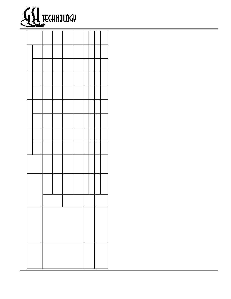
Synchronous Truth Table
Operation
Address
Used
State
Diagram
Key
5
E
1
E
2
ADSP ADSC
ADV
W
3
DQ
4
Deselect Cycle, Power Down
None
X
H
X
X
L
X
X
High-Z
Deselect Cycle, Power Down
None
X
L
F
L
X
X
X
High-Z
Deselect Cycle, Power Down
None
X
L
F
H
L
X
X
High-Z
Read Cycle, Begin Burst
External
R
L
T
L
X
X
X
Q
Read Cycle, Begin Burst
External
R
L
T
H
L
X
F
Q
Write Cycle, Begin Burst
External
W
L
T
H
L
X
T
D
Read Cycle, Continue Burst
Next
CR
X
X
H
H
L
F
Q
Read Cycle, Continue Burst
Next
CR
H
X
X
H
L
F
Q
Write Cycle, Continue Burst
Next
CW
X
X
H
H
L
T
D
Write Cycle, Continue Burst
Next
CW
H
X
X
H
L
T
D
Read Cycle, Suspend Burst
Current
X
X
H
H
H
F
Q
Read Cycle, Suspend Burst
Current
H
X
X
H
H
F
Q
Write Cycle, Suspend Burst
Current
X
X
H
H
H
T
D
Write Cycle, Suspend Burst
Current
H
X
X
H
H
T
D
Notes:
1. X = Don't Care, H = High, L = Low
2. E = T (True) if E
2
= 1 and E
3
= 0; E = F (False) if E
2
= 0 or E
3
= 1
3. W = T (True) and F (False) is defined in the Byte Write Truth Table preceding.
4. G is an asynchronous input. G can be driven high at any time to disable active output drivers. G low can only enable active drivers (shown
as "Q" in the Truth Table above).
5. All input combinations shown above are tested and supported. Input combinations shown in gray boxes need not be used to accomplish
basic synchronous or synchronous burst operations and may be avoided for simplicity.
6. Tying ADSP high and ADSC low allows simple non-burst synchronous operations. See BOLD items above.
7. Tying ADSP high and ADV low while using ADSC to load new addresses allows simple burst operations. See ITALIC items above.
Rev: 1.03a 5/2003
10/23
© 2001, Giga Semiconductor, Inc.
Specifications cited are subject to change without notice. For latest documentation see http://www.gsitechnology.com.
GS816018/32/36AT-300/250/200/150
Preliminary
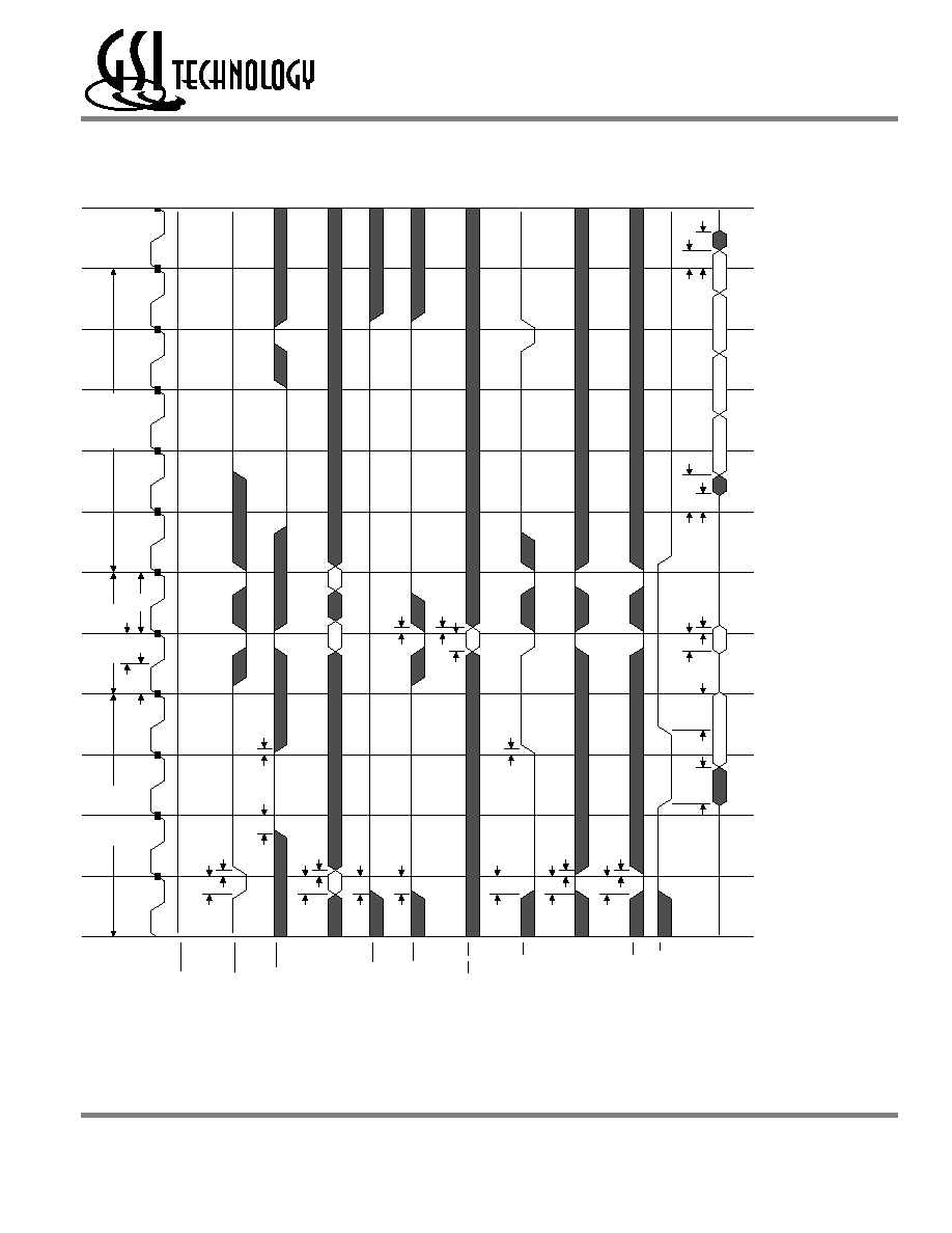
First Write
First Read
Burst Write
Burst Read
Deselect
R
W
CR
CW
X
X
W
R
R
W
R
X
X
X
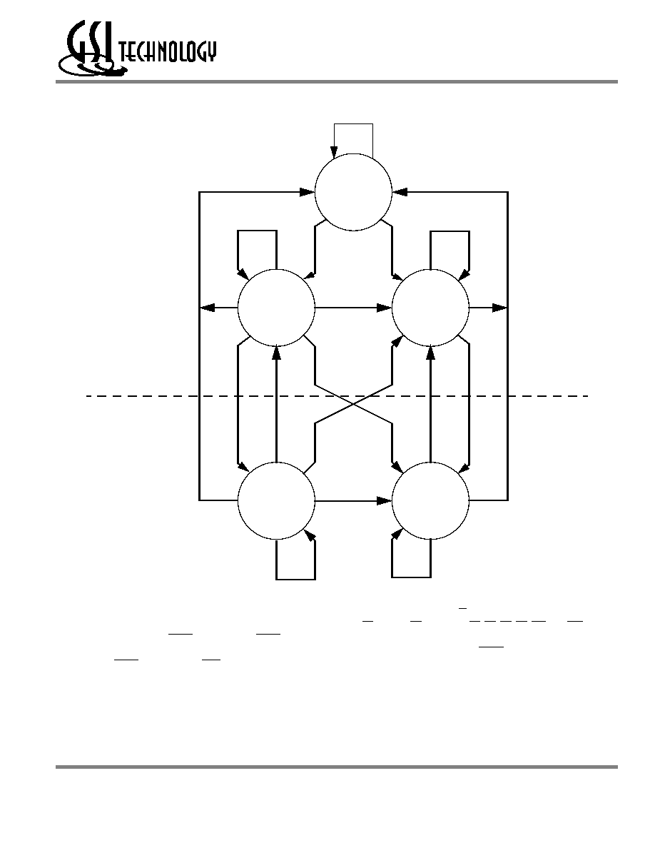
Simple Synchronous Operation
Simple Burst Synchronou
s Operation
CR
R
CW
CR
CR
Simplified State Diagram
Notes:
1. The diagram shows only supported (tested) synchronous state transitions. The diagram presumes G is tied low.
2. The upper portion of the diagram assumes active use of only the Enable (E1, E2, and E3) and Write (B
A
, B
B
, B
C
, B
D
, BW, and GW)
control inputs, and that ADSP is tied high and ADSC is tied low.
3. The upper and lower portions of the diagram together assume active use of only the Enable, Write, and ADSC control inputs, and
assumes ADSP is tied high and ADV is tied low.
Rev: 1.03a 5/2003
11/23
© 2001, Giga Semiconductor, Inc.
Specifications cited are subject to change without notice. For latest documentation see http://www.gsitechnology.com.
GS816018/32/36AT-300/250/200/150
Preliminary
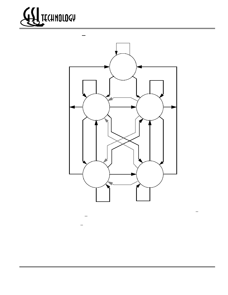
First Write
First Read
Burst Write
Burst Read
Deselect
R
W
CR
CW
X
X
W
R
R
W
R
X
X
X
CR
R
CW
CR
CR
W
CW
W
CW
Simplified State Diagram with G
Notes:
1. The diagram shows supported (tested) synchronous state transitions plus supported transitions that depend upon the use of G.
2. Use of "Dummy Reads" (Read Cycles with G High) may be used to make the transition from Read cycles to Write cycles without passing
through a Deselect cycle. Dummy Read cycles increment the address counter just like normal read cycles.
3. Transitions shown in gray tone assume G has been pulsed high long enough to turn the RAM's drivers off and for incoming data to meet
Data Input Set Up Time.
Rev: 1.03a 5/2003
12/23
© 2001, Giga Semiconductor, Inc.
Specifications cited are subject to change without notice. For latest documentation see http://www.gsitechnology.com.
GS816018/32/36AT-300/250/200/150
Preliminary
Note:
Permanent damage to the device may occur if the Absolute Maximum Ratings are exceeded. Operation should be restricted to Recommended Operating Condi-
tions. Exposure to conditions exceeding the Absolute Maximum Ratings, for an extended period of time, may affect reliability of this component.
Absolute Maximum Ratings
(All voltages reference to V
SS
)
Symbol
Description
Value
Unit
V
DD
Voltage on V
DD
Pins
≠0.5 to 4.6
V
V
DDQ
Voltage in V
DDQ
Pins
≠0.5 to 4.6
V
V
I/O
Voltage on I/O Pins
≠0.5 to V
DDQ
+0.5 (
4.6 V max.)
V
V
IN
Voltage on Other Input Pins
≠0.5 to V
DD
+0.5 (
4.6 V max.)
V
I
IN
Input Current on Any Pin
+/≠20
mA
I
OUT
Output Current on Any I/O Pin
+/≠20
mA
P
D
Package Power Dissipation
1.5
W
T
STG
Storage Temperature
≠55 to 125
o
C
T
BIAS
Temperature Under Bias
≠55 to 125
o
C
Rev: 1.03a 5/2003
13/23
© 2001, Giga Semiconductor, Inc.
Specifications cited are subject to change without notice. For latest documentation see http://www.gsitechnology.com.
GS816018/32/36AT-300/250/200/150
Preliminary
Power Supply Voltage Ranges
Parameter
Symbol
Min.
Typ.
Max.
Unit
Notes
3.3 V Supply Voltage
V
DD3
3.0
3.3
3.6
V
2.5 V Supply Voltage
V
DD2
2.3
2.5
2.7
V
3.3 V V
DDQ
I/O Supply Voltage
V
DDQ3
3.0
3.3
3.6
V
2.5 V V
DDQ
I/O Supply Voltage
V
DDQ2
2.3
2.5
2.7
V
Notes:
1.
The part numbers of Industrial Temperature Range versions end the character "I". Unless otherwise noted, all performance specifications quoted are
evaluated for worst case in the temperature range marked on the device.
2.
Input Under/overshoot voltage must be ≠2 V > Vi < V
DDn
+2 V not to exceed 4.6 V maximum, with a pulse width not to exceed 20% tKC.
V
DDQ3
Range Logic Levels
Parameter
Symbol
Min.
Typ.
Max.
Unit
Notes
V
DD
Input High Voltage
V
IH
2.0
--
V
DD
+ 0.3
V
1
V
DD
Input Low Voltage
V
IL
≠0.3
--
0.8
V
1
V
DDQ
I/O Input High Voltage
V
IHQ
2.0
--
V
DDQ
+ 0.3
V
1,3
V
DDQ
I/O Input Low Voltage
V
ILQ
≠0.3
--
0.8
V
1,3
Notes:
1.
The part numbers of Industrial Temperature Range versions end the character "I". Unless otherwise noted, all performance specifications quoted are
evaluated for worst case in the temperature range marked on the device.
2.
Input Under/overshoot voltage must be ≠2 V > Vi < V
DDn
+2 V not to exceed 4.6 V maximum, with a pulse width not to exceed 20% tKC.
3.
V
IHQ
(max) is voltage on V
DDQ
pins plus 0.3 V.
V
DDQ2
Range Logic Levels
Parameter
Symbol
Min.
Typ.
Max.
Unit
Notes
V
DD
Input High Voltage
V
IH
0.6*V
DD
--
V
DD
+ 0.3
V
1
V
DD
Input Low Voltage
V
IL
≠0.3
--
0.3*V
DD
V
1
V
DDQ
I/O Input High Voltage
V
IHQ
0.6*V
DD
--
V
DDQ
+ 0.3
V
1,3
V
DDQ
I/O Input Low Voltage
V
ILQ
≠0.3
--
0.3*V
DD
V
1,3
Notes:
1.
The part numbers of Industrial Temperature Range versions end the character "I". Unless otherwise noted, all performance specifications quoted are
evaluated for worst case in the temperature range marked on the device.
2.
Input Under/overshoot voltage must be ≠2 V > Vi < V
DDn
+2 V not to exceed 4.6 V maximum, with a pulse width not to exceed 20% tKC.
3.
V
IHQ
(max) is voltage on V
DDQ
pins plus 0.3 V.

Rev: 1.03a 5/2003
14/23
© 2001, Giga Semiconductor, Inc.
Specifications cited are subject to change without notice. For latest documentation see http://www.gsitechnology.com.
GS816018/32/36AT-300/250/200/150
Preliminary
Note: These parameters are sample tested.
Recommended Operating Temperatures
Parameter
Symbol
Min.
Typ.
Max.
Unit
Notes
Ambient Temperature (Commercial Range Versions)
T
A
0
25
70
∞
C
2
Ambient Temperature (Industrial Range Versions)
T
A
≠40
25
85
∞
C
2
Note:
1.
The part numbers of Industrial Temperature Range versions end the character "I". Unless otherwise noted, all performance specifications quoted are
evaluated for worst case in the temperature range marked on the device.
2.
Input Under/overshoot voltage must be ≠2 V > Vi < V
DDn
+2 V not to exceed 4.6 V maximum, with a pulse width not to exceed 20% tKC.
Capacitance
(T
A
= 25
o
C, f = 1 MH
Z
, V
DD
= 2.5 V)
Parameter
Symbol
Test conditions
Typ.
Max.
Unit
Input Capacitance
C
IN
V
IN
= 0 V
4
5
pF
Input/Output Capacitance
C
I/O
V
OUT
= 0 V
6
7
pF
20% tKC
V
SS
≠ 2.0 V
50%
V
SS
V
IH
Undershoot Measurement and Timing
Overshoot Measurement and Timing
20% tKC
V
DD
+ 2.0 V
50%
V
DD
V
IL

Rev: 1.03a 5/2003
15/23
© 2001, Giga Semiconductor, Inc.
Specifications cited are subject to change without notice. For latest documentation see http://www.gsitechnology.com.
GS816018/32/36AT-300/250/200/150
Preliminary
AC Test Conditions
Parameter
Conditions
Input high level
V
DD
≠ 0.2 V
Input low level
0.2 V
Input slew rate
1 V/ns
Input reference level
V
DD
/2
Output reference level
V
DDQ
/2
Output load
Fig. 1
Notes:
1. Include scope and jig capacitance.
2. Test conditions as specified with output loading as shown in Fig. 1
unless otherwise noted.
3. Device is deselected as defined by the Truth Table.
DC Electrical Characteristics
Parameter
Symbol
Test Conditions
Min
Max
Input Leakage Current
(except mode pins)
I
IL
V
IN
= 0 to V
DD
≠1 uA
1 uA
ZZ Input Current
I
IN1
V
DD
V
IN
V
IH
0 V
V
IN
V
IH
≠1 uA
≠1 uA
1 uA
100 uA
FT Input Current
I
IN2
V
DD
V
IN
V
IL
0 V
V
IN
V
IL
≠100 uA
≠1 uA
1 uA
1 uA
Output Leakage Current
I
OL
Output Disable, V
OUT
= 0 to V
DD
≠1 uA
1 uA
Output High Voltage
V
OH2
I
OH
= ≠8 mA, V
DDQ
= 2.375 V
1.7 V
--
Output High Voltage
V
OH3
I
OH
= ≠8 mA, V
DDQ
= 3.135 V
2.4 V
--
Output Low Voltage
V
OL
I
OL
= 8 mA
--
0.4 V
DQ
V
DDQ/2
50
30pF
*
Output Load 1
* Distributed Test Jig Capacitance
Rev: 1.03a 5/2003
16/23
© 2001, Giga Semiconductor, Inc.
Specifications cited are subject to change without notice. For latest documentation see http://www.gsitechnology.com.
GS816018/32/36AT-300/250/200/150
Preliminary
Operating Cu
rrents
Notes:
1.
I
DD
and I
DDQ
apply to any combination of V
DD3
, V
DD2
, V
DDQ3
, and
V
DD
Q
2
operation.
2.
All parameters listed are worst case scenario.
Parameter
T
est
Condi
t
i
ons
Mode
Sym
bol
-300
-250
-200
-
1
50
Unit
0
to 70∞C
≠
40
to 85∞C
0
to 70∞C
≠
40
to
85∞C
0
to 70∞C
≠
40
to 85∞C
0
to 70∞C
≠
40
to 85∞C
Operat
in
g
Current
Dev
i
ce Sel
e
ct
ed;
All oth
e
r inputs
V
IH
o
r
V
IL
Outpu
t
open
(x
32/
x36)
Pipeline
I
DD
I
DDQ
345
45
35
5
45
29
0
40
300
40
240
30
250
30
19
0
20
20
0
20
mA
Flow Through
I
DD
I
DDQ
240
30
25
0
30
22
0
20
230
20
190
15
200
15
17
5
15
18
5
15
mA
(x
18)
Pipeline
I
DD
I
DDQ
310
25
32
0
25
26
0
20
270
20
215
15
225
15
17
0
15
18
0
15
mA
Flow Through
I
DD
I
DDQ
215
15
22
5
15
20
0
10
210
10
175
10
185
10
16
0
10
17
0
10
mA
St
and
by
Current
ZZ
V
DD
≠ 0.2 V
--
Pipeline
I
SB
40
50
40
50
4
0
50
40
50
m
A
Flow Through
I
SB
40
50
40
50
4
0
50
40
50
m
A
De
selec
t
Current
Devi
c
e
D
e
sel
e
c
t
e
d
;
All oth
e
r inputs
V
IH
or
V
IL
--
Pipeline
I
DD
85
90
85
90
7
5
80
60
65
m
A
Flow Through
I
DD
60
65
60
65
5
0
55
50
55
m
A

Rev: 1.03a 5/2003
17/23
© 2001, Giga Semiconductor, Inc.
Specifications cited are subject to change without notice. For latest documentation see http://www.gsitechnology.com.
GS816018/32/36AT-300/250/200/150
Preliminary
AC Electrical Characteristics
Notes:
1. These parameters are sampled and are not 100% tested.
2. ZZ is an asynchronous signal. However, in order to be recognized on any given clock cycle, ZZ must meet the specified setup and hold times
as specified above.
Parameter
Symbol
-300
-250
-200
-150
Unit
Min
Max
Min
Max
Min
Max
Min
Max
Pipeline
Clock Cycle Time
tKC
3.3
--
4.0
--
5.0
--
6.7
--
ns
Clock to Output Valid
tKQ
--
2.5
--
2.5
--
3.0
--
3.8
ns
Clock to Output Invalid
tKQX
1.5
--
1.5
--
1.5
--
1.5
--
ns
Clock to Output in Low-Z
tLZ
1
1.5
--
1.5
--
1.5
--
1.5
--
ns
Setup time
tS
1.0
--
1.2
--
1.4
--
1.5
--
ns
Hold time
tH
0.1
--
0.2
--
0.4
--
0.5
--
ns
Flow Through
Clock Cycle Time
tKC
5.0
--
5.5
--
6.5
--
7.5
--
ns
Clock to Output Valid
tKQ
--
5.0
--
5.5
--
6.5
--
7.5
ns
Clock to Output Invalid
tKQX
3.0
--
3.0
--
3.0
--
3.0
--
ns
Clock to Output in Low-Z
tLZ
1
3.0
--
3.0
--
3.0
--
3.0
--
ns
Setup time
tS
1.4
--
1.5
--
1.5
--
1.5
--
ns
Hold time
tH
0.4
--
0.5
--
0.5
--
0.5
--
ns
Clock HIGH Time
tKH
1.3
--
1.3
--
1.3
--
1.5
--
ns
Clock LOW Time
tKL
1.5
--
1.5
--
1.5
--
1.7
--
ns
Clock to Output in
High-Z
tHZ
1
1.5 2.5
1.5 2.5
1.5 3.0
1.5 3.0
ns
G to Output Valid
tOE
--
2.5
--
2.5
--
3.0
--
3.8
ns
G to output in Low-Z
tOLZ
1
0
--
0
--
0
--
0
--
ns
G to output in High-Z
tOHZ
1
--
2.5
--
2.5
--
3.0
--
3.8
ns
ZZ setup time
tZZS
2
5
--
5
--
5
--
5
--
ns
ZZ hold time
tZZH
2
1
--
1
--
1
--
1
--
ns
ZZ recovery
tZZR
20
--
20
--
20
--
20
--
ns
Rev: 1.03a 5/2003
18/23
© 2001, Giga Semiconductor, Inc.
Specifications cited are subject to change without notice. For latest documentation see http://www.gsitechnology.com.
GS816018/32/36AT-300/250/200/150
Preliminary
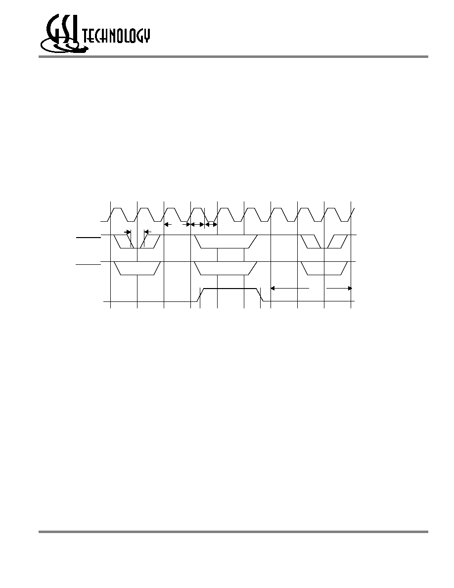
Pipeline Mode Timing
Begi
n
R
ea
d A
C
ont
Cont
D
e
s
e
lec
t
Writ
e B
R
e
a
d C
R
e
a
d C+1
R
e
a
d C+2
R
ea
d C+3
C
ont
Desele
ct
tH
Z
tK
QX
tK
Q
tL
Z
tH
tS
tO
HZ
tO
E
tH
tS
tH
tS
tH
tS
tH
tS
tH
tS
tS
tH
tS
tH
tS
tH
tS
Burst Rea
d
Burst Rea
d
S
i
ngle W
r
it
e
tK
C
tK
C
tK
L
tK
L
tK
H
S
i
ngle W
r
it
e
Si
ngle Re
ad
tK
H
Si
ngle Re
ad
Q(A)
D(
B
)
Q(
C
)
Q(C+1
)
Q
(
C+
2)
Q(C+3)
AB
C
De
se
le
ct
ed
wit
h
E1
E1 m
a
sk
s A
D
S
P
E2
and
E
3
only
samp
l
e
d
wit
h
ADSP
and
AD
SC
ADSC i
n
i
tia
te
d
re
ad
CK
ADS
P
AD
SC
ADV
A0
≠
A
n
GW
BW
Ba
≠Bd
E1
E2
E3
G
DQa≠DQ
d

Rev: 1.03a 5/2003
19/23
© 2001, Giga Semiconductor, Inc.
Specifications cited are subject to change without notice. For latest documentation see http://www.gsitechnology.com.
GS816018/32/36AT-300/250/200/150
Preliminary
Flow Through Mode Timing
Begin
R
ead A
C
on
t
C
ont
1
W
rit
e
B
R
ead C
R
e
a
d C+1
R
ea
d C+
2
R
ead C+3
R
e
a
d C
C
ont2
D
e
s
e
l
ec
t
tH
Z
tK
QX
tK
Q
tL
Z
tH
tS
tO
HZ
tO
E
tH
tS
tH
tS
tH
tS
tH
tS
tH
tS
tH
tS
tH
tS
tH
tS
tH
tS
tH
tS
tK
C
tK
C
tK
L
tK
L
tK
H
tK
H
AB
C
Q(A)
D(
B
)
Q(C)
Q(
C+
1)
Q(C+2
)
Q(C+3
)
Q(C)
E2 an
d E
3
o
n
l
y
sa
mple
d
with
ADSC
ADSC i
n
it
ia
te
d r
e
a
d
De
se
l
ect
ed
wit
h
E1
Fix
e
d H
i
gh
CK
AD
SP
AD
S
C
AD
V
A0≠An
GW
BW
Ba
≠Bd
E1
E2
E3
G
D
Q
a≠DQd
Rev: 1.03a 5/2003
20/23
© 2001, Giga Semiconductor, Inc.
Specifications cited are subject to change without notice. For latest documentation see http://www.gsitechnology.com.
GS816018/32/36AT-300/250/200/150
Preliminary
Sleep Mode
During normal operation, ZZ must be pulled low, either by the user or by its internal pull down resistor. When ZZ is pulled high,
the SRAM will enter a Power Sleep mode after 2 cycles. At this time, internal state of the SRAM is preserved. When ZZ returns to
low, the SRAM operates normally after ZZ recovery time.
Sleep mode is a low current, power-down mode in which the device is deselected and current is reduced to I
SB
2. The duration of
Sleep mode is dictated by the length of time the ZZ is in a High state. After entering Sleep mode, all inputs except ZZ become
disabled and all outputs go to High-Z The ZZ pin is an asynchronous, active high input that causes the device to enter Sleep mode.
When the ZZ pin is driven high, I
SB
2 is guaranteed after the time tZZI is met. Because ZZ is an asynchronous input, pending
operations or operations in progress may not be properly completed if ZZ is asserted. Therefore, Sleep mode must not be initiated
until valid pending operations are completed. Similarly, when exiting Sleep mode during tZZR, only a Deselect or Read commands
may be applied while the SRAM is recovering from Sleep mode.
Application Tips
Single and Dual Cycle Deselect
SCD devices (like this one) force the use of "dummy read cycles" (read cycles that are launched normally but that are ended with
the output drivers inactive) in a fully synchronous environment. Dummy read cycles waste performance but their use usually
assures there will be no bus contention in transitions from reads to writes or between banks of RAMs. DCD SRAMs do not waste
bandwidth on dummy cycles and are logically simpler to manage in a multiple bank application (wait states need not be inserted at
bank address boundary crossings) but greater care must be exercised to avoid excessive bus contention.
CK
ADSP
ADSC
tH
tKH tKL
tKC
tS
ZZ
tZZR
tZZH
tZZS
~ ~
~ ~
~ ~
~ ~
~ ~
~ ~
Snooze
Sleep Mode Timing Diagram
~ ~
~ ~
~ ~
~ ~
~ ~
Rev: 1.03a 5/2003
21/23
© 2001, Giga Semiconductor, Inc.
Specifications cited are subject to change without notice. For latest documentation see http://www.gsitechnology.com.
GS816018/32/36AT-300/250/200/150
Preliminary
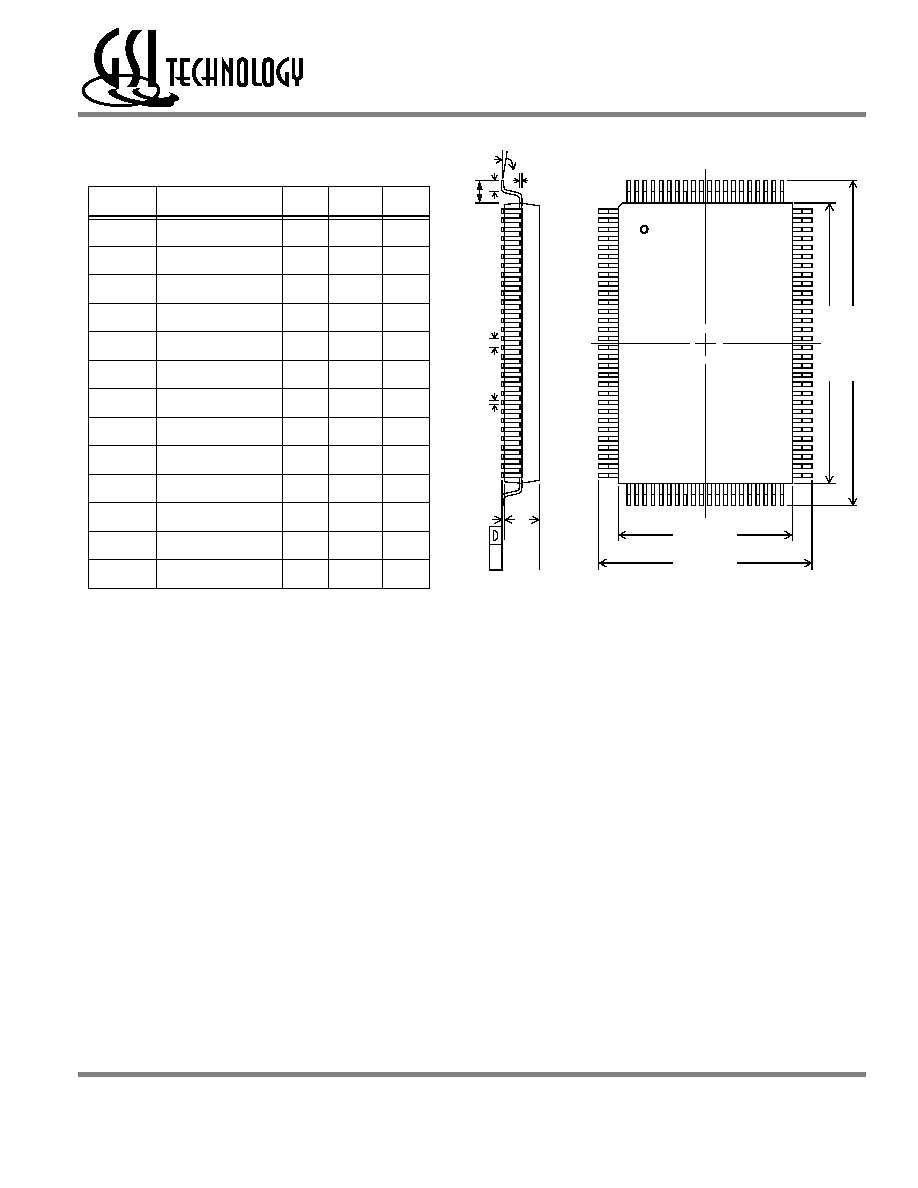
TQFP Package Drawing
D1
D
E1
E
Pin 1
b
e
c
L
L1
A2
A1
Y
Notes:
1. All dimensions are in millimeters (mm).
2. Package width and length do not include mold protrusion.
Symbol
Description
Min. Nom. Max
A1
Standoff
0.05
0.10
0.15
A2
Body Thickness
1.35
1.40
1.45
b
Lead Width
0.20
0.30
0.40
c
Lead Thickness
0.09
--
0.20
D
Terminal Dimension
21.9
22.0
22.1
D1
Package Body
19.9
20.0
20.1
E
Terminal Dimension
15.9
16.0
16.1
E1
Package Body
13.9
14.0
14.1
e
Lead Pitch
--
0.65
--
L
Foot Length
0.45
0.60
0.75
L1
Lead Length
--
1.00
--
Y
Coplanarity
0.10
Lead Angle
0
∞
--
7
∞
Rev: 1.03a 5/2003
22/23
© 2001, Giga Semiconductor, Inc.
Specifications cited are subject to change without notice. For latest documentation see http://www.gsitechnology.com.
GS816018/32/36AT-300/250/200/150
Preliminary
Ordering Information for GSI Synchronous Burst RAMs
Org
Part Number
1
Type
Package
Speed
2
(MHz/ns)
T
A
3
Status
1M x 18
GS816018AT-300
Pipeline/Flow Through
TQFP
300/5
C
1M x 18
GS816018AT-250
Pipeline/Flow Through
TQFP
250/5.5
C
1M x 18
GS816018AT-200
Pipeline/Flow Through
TQFP
200/6.5
C
1M x 18
GS816018AT-150
Pipeline/Flow Through
TQFP
150/7.5
C
512K x 32
GS816032AT-300
Pipeline/Flow Through
TQFP
300/5
C
512K x 32
GS816032AT-250
Pipeline/Flow Through
TQFP
250/5.5
C
512K x 32
GS816032AT-200
Pipeline/Flow Through
TQFP
200/6.5
C
512K x 32
GS816032AT-150
Pipeline/Flow Through
TQFP
150/7.5
C
512K x 36
GS816036AT-300
Pipeline/Flow Through
TQFP
300/5
C
512K x 36
GS816036AT-250
Pipeline/Flow Through
TQFP
250/5.5
C
512K x 36
GS816036AT-200
Pipeline/Flow Through
TQFP
200/6.5
C
512K x 36
GS816036AT-150
Pipeline/Flow Through
TQFP
150/7.5
C
1M x 18
GS816018AT-300I
Pipeline/Flow Through
TQFP
300/5
I
1M x 18
GS816018AT-250I
Pipeline/Flow Through
TQFP
250/5.5
I
1M x 18
GS816018AT-200I
Pipeline/Flow Through
TQFP
200/6.5
I
1M x 18
GS816018AT-150I
Pipeline/Flow Through
TQFP
150/7.5
I
512K x 32
GS816032AT-300I
Pipeline/Flow Through
TQFP
300/5
I
512K x 32
GS816032AT-250I
Pipeline/Flow Through
TQFP
250/5.5
I
512K x 32
GS816032AT-200I
Pipeline/Flow Through
TQFP
200/6.5
I
512K x 32
GS816032AT-150I
Pipeline/Flow Through
TQFP
150/7.5
I
512K x 36
GS816036AT-300I
Pipeline/Flow Through
TQFP
300/5
I
512K x 36
GS816036AT-250I
Pipeline/Flow Through
TQFP
250/5.5
I
512K x 36
GS816036AT-200I
Pipeline/Flow Through
TQFP
200/6.5
I
512K x 36
GS816036AT-150I
Pipeline/Flow Through
TQFP
150/7.5
I
Notes:
1. Customers requiring delivery in Tape and Reel should add the character "T" to the end of the part number. Example: GS816018AT-150IT.
2. The speed column indicates the cycle frequency (MHz) of the device in Pipeline mode and the latency (ns) in Flow Through mode. Each
device is Pipeline/Flow through mode-selectable by the user.
3. T
A
= C = Commercial Temperature Range. T
A
= I = Industrial Temperature Range.
4. GSI offers other versions this type of device in many different configurations and with a variety of different features, only some of which
are covered in this data sheet. See the GSI Technology web site (www.gsitechnology.com) for a complete listing of current offerings.
Rev: 1.03a 5/2003
23/23
© 2001, Giga Semiconductor, Inc.
Specifications cited are subject to change without notice. For latest documentation see http://www.gsitechnology.com.
GS816018/32/36AT-300/250/200/150
Preliminary
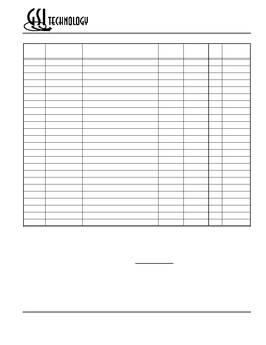
18Mb Sync SRAM Datasheet Revision History
DS/DateRev. Code: Old;
New
Types of Changes
Format or Content
Page;Revisions;Reason
816018A_r1
∑ Creation of new datasheet
816018A_r1;
816018A_r1_01
Content
∑ Updated FT power numbers
∑ Updated AC Characteristics table
∑ Updated ZZ recovery time diagram
∑ Updated AC Test Conditions table and removed Output Load
2 diagram
816018A_r1_01;
816018A_r1_02
Content
∑ Removed extraneous V
DDQ1
table on page 13 and changed
V
DDQ2
table to V
DDQ
∑ Removed pin locations from pin description table
8160xxA_r1_02;
8160xxA_r1_03
Content
∑ Entire datasheet was rewritten due to design changes