 | –≠–ª–µ–∫—Ç—Ä–æ–Ω–Ω—ã–π –∫–æ–º–ø–æ–Ω–µ–Ω—Ç: GS8161Z18 | –°–∫–∞—á–∞—Ç—å:  PDF PDF  ZIP ZIP |

Rev: 2.13a 1/2003
1/39
© 1998, Giga Semiconductor, Inc.
Specifications cited are subject to change without notice. For latest documentation see http://www.gsitechnology.com.
NoBL is a trademark of Cypress Semiconductor Corp.. NtRAM is a trademark of Samsung Electronics Co.. ZBT is a trademark of Integrated Device Technology, Inc.
GS8161Z18(T/D)/GS8161Z32(D)/GS8161Z36(T/D)
18Mb Pipelined and Flow Through
Synchronous NBT SRAM
250 MHz≠133 MHz
2.5 V or 3.3 V V
DD
2.5 V or 3.3 V I/O
100-Pin TQFP
Commercial Temp
Industrial Temp
Features
∑ User-configurable Pipeline and Flow Through mode
∑ NBT (No Bus Turn Around) functionality allows zero wait
read-write-read bus utilization
∑ Fully pin-compatible with both pipelined and flow through
NtRAMTM, NoBLTM and ZBTTM SRAMs
∑ IEEE 1149.1 JTAG-compatible Boundary Scan
∑ 2.5 V or 3.3 V +10%/≠10% core power supply
∑ LBO pin for Linear or Interleave Burst mode
∑ Pin-compatible with 2M, 4M, and 8M devices
∑ Byte write operation (9-bit Bytes)
∑ 3 chip enable signals for easy depth expansion
∑ ZZ pin for automatic power-down
∑ JEDEC-standard 100-lead TQFP and 165-bump FP-BGA
packages
Functional Description
The GS8161Z18(T/D)/GS8161Z32(D)/GS8161Z36(T/D) is an
18Mbit Synchronous Static SRAM. GSI's NBT SRAMs, like
ZBT, NtRAM, NoBL or other pipelined read/double late write
or flow through read/single late write SRAMs, allow
utilization of all available bus bandwidth by eliminating the
need to insert deselect cycles when the device is switched from
read to write cycles.
Because it is a synchronous device, address, data inputs, and
read/ write control inputs are captured on the rising edge of the
input clock. Burst order control (LBO) must be tied to a power
rail for proper operation. Asynchronous inputs include the
Sleep mode enable, ZZ and Output Enable. Output Enable can
be used to override the synchronous control of the output
drivers and turn the RAM's output drivers off at any time.
Write cycles are internally self-timed and initiated by the rising
edge of the clock input. This feature eliminates complex off-
chip write pulse generation required by asynchronous SRAMs
and simplifies input signal timing.
The GS8161Z18(T/D)/GS8161Z32(D)/GS8161Z36(T/D) may
be configured by the user to operate in Pipeline or Flow
Through mode. Operating as a pipelined synchronous device,
in addition to the rising-edge-triggered registers that capture
input signals, the device incorporates a rising-edge-triggered
output register. For read cycles, pipelined SRAM output data is
temporarily stored by the edge triggered output register during
the access cycle and then released to the output drivers at the
next rising edge of clock.
The GS8161Z18(T/D)/GS8161Z32(D)/GS8161Z36(T/D) is
implemented with GSI's high performance CMOS technology
and is available in JEDEC-standard 100-pin TQFP and
165-bump FP-BGA packages.
-250 -225 -200 -166 -150 -133 Unit
Pipeline
3-1-1-1
t
KQ
tCycle
2.5
4.0
2.7
4.4
3.0
5.0
3.4
6.0
3.8
6.7
4.0
7.5
ns
ns
3.3 V
Curr
(x18)
Curr
(x32/x36)
280
330
255
300
230
270
200
230
185
215
165
190
mA
mA
2.5 V
Curr
(x18)
Curr
(x32/x36)
275
320
250
295
230
265
195
225
180
210
165
185
mA
mA
Flow
Through
2-1-1-1
t
KQ
tCycle
5.5
5.5
6.0
6.0
6.5
6.5
7.0
7.0
7.5
7.5
8.5
8.5
ns
ns
3.3 V
Curr
(x18)
Curr
(x32/x36)
175
200
165
190
160
180
150
170
145
165
135
150
mA
mA
2.5 V
Curr
(x18)
Curr
(x32/x36)
175
200
165
190
160
180
150
170
145
165
135
150
mA
mA

Rev: 2.13a 1/2003
2/39
© 1998, Giga Semiconductor, Inc.
Specifications cited are subject to change without notice. For latest documentation see http://www.gsitechnology.com.
GS8161Z18(T/D)/GS8161Z32(D)/GS8161Z36(T/D)
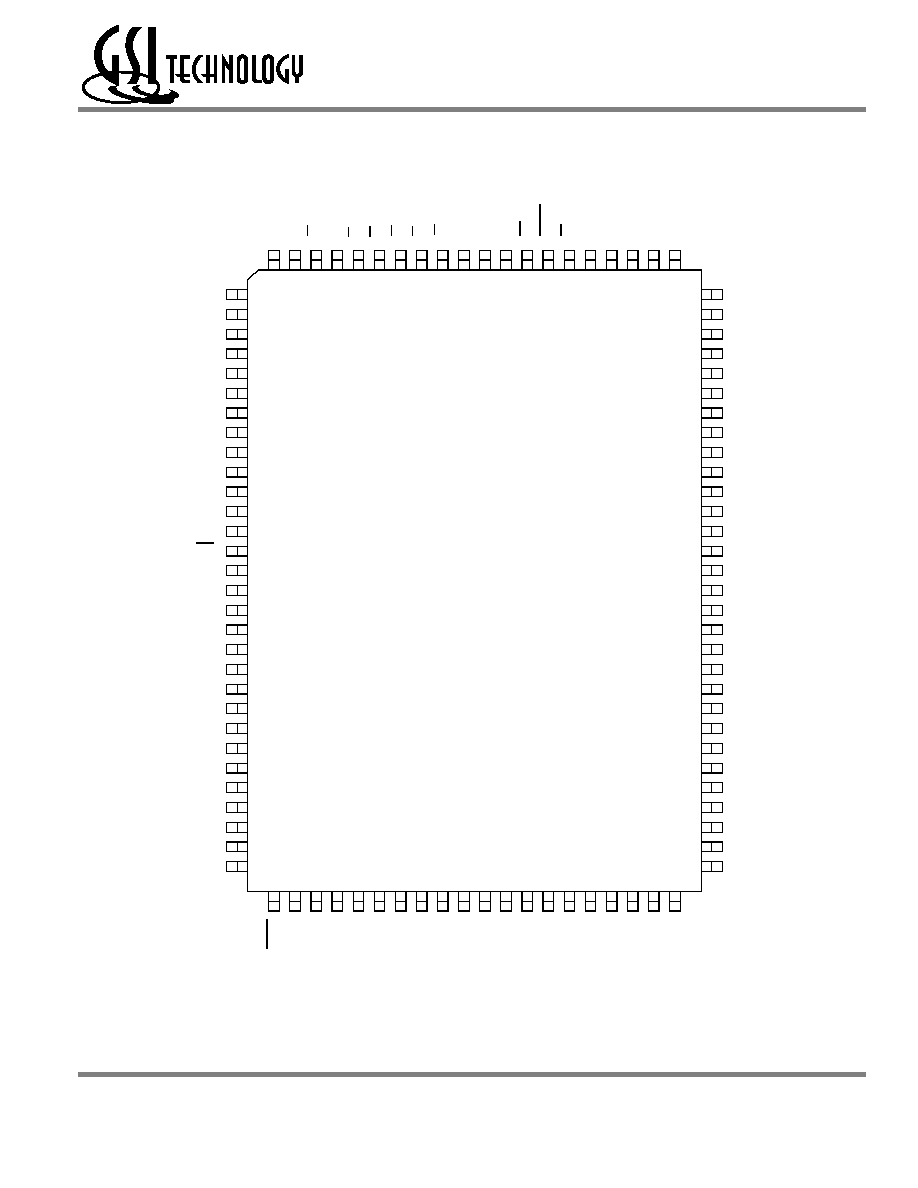
GS8161Z18T Pinout
80
79
78
77
76
75
74
73
72
71
70
69
68
67
66
65
64
63
62
61
60
59
58
57
56
55
54
53
52
51
1
2
3
4
5
6
7
8
9
10
11
12
13
14
15
16
17
18
19
20
21
22
23
24
25
26
27
28
29
30
V
DDQ
V
SS
DQ
B1
DQ
B2
V
SS
V
DDQ
DQ
B3
DQ
B4
FT
V
DD
NC
V
SS
DQ
B5
DQ
B6
V
DDQ
V
SS
DQ
B7
DQ
B8
DQ
B9
V
SS
V
DDQ
V
DDQ
V
SS
DQ
A8
DQ
A7
V
SS
V
DDQ
DQ
A6
DQ
A5
V
SS
NC
V
DD
ZZ
DQ
A4
DQ
A3
V
DDQ
V
SS
DQ
A2
DQ
A1
V
SS
V
DDQ
LB
O
A
5
A
4
A
3
A
2
A
1
A
0
TMS
TD
I
V
SS
V
DD
TDO
TCK
A
10
A
11
A
12
A
13
A
14
A
16
A
6
A
7
E
1
E
2
NC
NC
B
B
B
A
E
3
CK
W
CKE
V
DD
V
SS
G
ADV
A
18
A
17
A
8
A
9
A
15
1M x 18
Top View
DQ
A9
A
19
NC
NC
NC
NC
NC
NC
NC
NC
NC
NC
NC
NC
NC
NC
NC
NC
NC
100 99 98 97 96 95 94 93 92 91 90 89 88 87 86 85 84 83 82 81
31 32 33 34 35 36 37 38 39 40 41 42 43 44 45 46 47 48 49 50
Rev: 2.13a 1/2003
3/39
© 1998, Giga Semiconductor, Inc.
Specifications cited are subject to change without notice. For latest documentation see http://www.gsitechnology.com.
GS8161Z18(T/D)/GS8161Z32(D)/GS8161Z36(T/D)
GS8161Z36T Pinout
80
79
78
77
76
75
74
73
72
71
70
69
68
67
66
65
64
63
62
61
60
59
58
57
56
55
54
53
52
51
1
2
3
4
5
6
7
8
9
10
11
12
13
14
15
16
17
18
19
20
21
22
23
24
25
26
27
28
29
30
V
DDQ
V
SS
DQ
C4
DQ
C3
V
SS
V
DDQ
DQ
C2
DQ
C1
FT
V
DD
NC
V
SS
DQ
D1
DQ
D2
V
DDQ
V
SS
DQ
D3
DQ
D4
DQ
D5
V
SS
V
DDQ
V
DDQ
V
SS
DQ
B4
DQ
B3
V
SS
V
DDQ
DQ
B2
DQ
B1
V
SS
NC
V
DD
ZZ
DQ
A1
DQ
A2
V
DDQ
V
SS
DQ
A3
DQ
A4
V
SS
V
DDQ
LB
O
A
5
A
4
A
3
A
2
A
1
A
0
TMS
TDI
V
SS
V
DD
TD
O
TCK
A
10
A
11
A
12
A
13
A
14
A
16
A
6
A
7
E
1
E
2
B
D
B
C
B
B
B
A
E
3
CK
W
CKE
V
DD
V
SS
G
ADV
A
18
A
17
A
8
A
9
A
15
512K x 36
Top View
DQ
B5
DQ
B9
DQ
B7
DQ
B8
DQ
B6
DQ
A6
DQ
A5
DQ
A8
DQ
A7
DQ
A9
DQ
C7
DQ
C8
DQ
C6
DQ
D6
DQ
D8
DQ
D7
DQ
D9
DQ
C5
DQ
C9
100 99 98 97 96 95 94 93 92 91 90 89 88 87 86 85 84 83 82 81
31 32 33 34 35 36 37 38 39 40 41 42 43 44 45 46 47 48 49 50
Rev: 2.13a 1/2003
4/39
© 1998, Giga Semiconductor, Inc.
Specifications cited are subject to change without notice. For latest documentation see http://www.gsitechnology.com.
GS8161Z18(T/D)/GS8161Z32(D)/GS8161Z36(T/D)
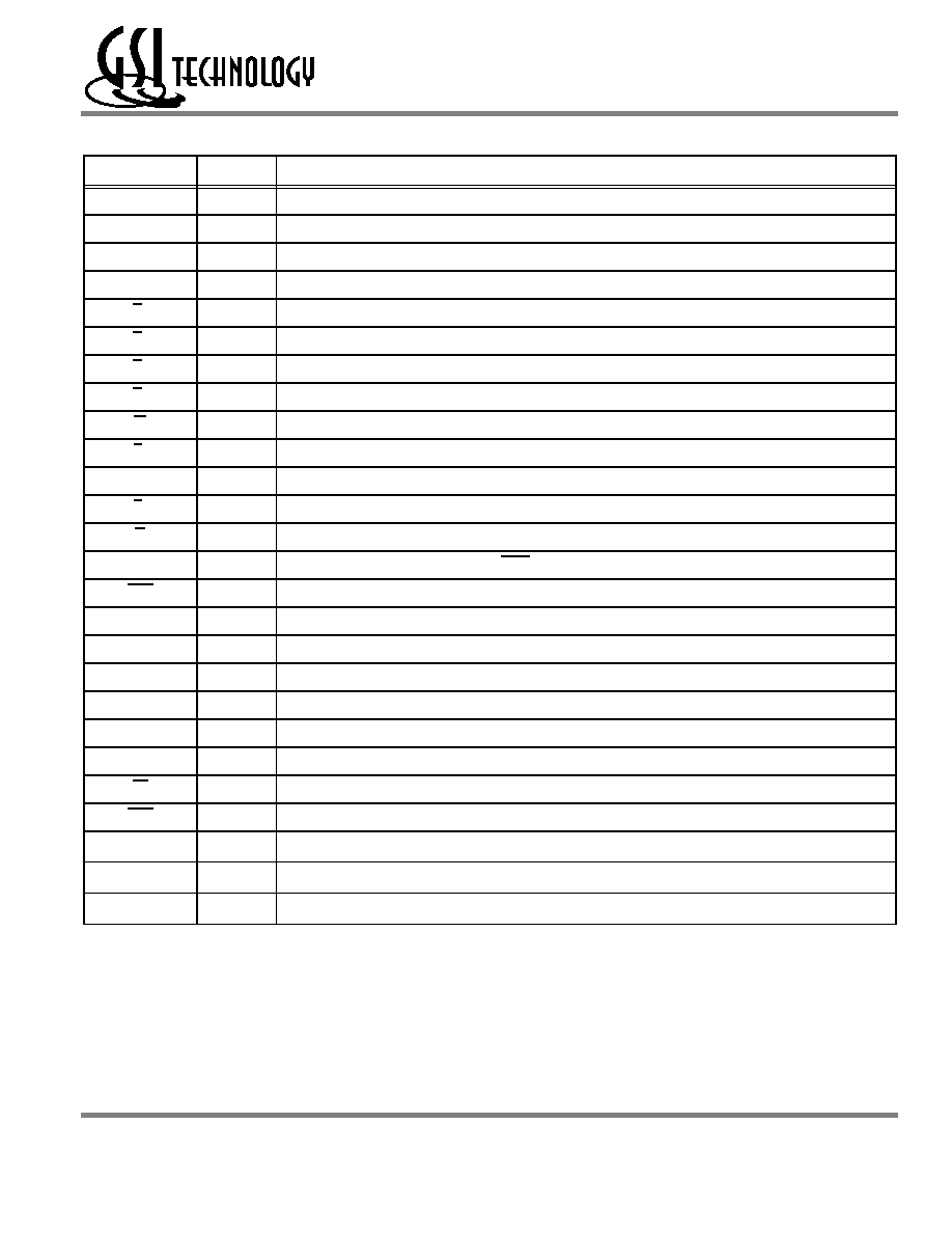
100-Pin TQFP Pin Descriptions
Symbol
Type
Description
A
0
, A
1
In
Burst Address Inputs; Preload the burst counter
A
2≠
A
18
In
Address Inputs
A
19
In
Address Input
CK
In
Clock Input Signal
B
A
In
Byte Write signal for data inputs DQ
A1
≠DQ
A9
; active low
B
B
In
Byte Write signal for data inputs DQ
B1
≠DQ
B9
; active low
B
C
In
Byte Write signal for data inputs DQ
C1
≠DQ
C9
; active low
B
D
In
Byte Write signal for data inputs DQ
D1
≠DQ
D9
; active low
W
In
Write Enable; active low
E
1
In
Chip Enable; active low
E
2
In
Chip Enable--Active High. For self decoded depth expansion
E
3
In
Chip Enable--Active Low. For self decoded depth expansion
G
In
Output Enable; active low
ADV
In
Advance/Load; Burst address counter control pin
CKE
In
Clock Input Buffer Enable; active low
NC
--
No Connect
DQ
A1
≠DQ
A9
I/O
Byte A Data Input and Output pins
DQ
B1
≠DQ
B9
I/O
Byte B Data Input and Output pins
DQ
C1
≠DQ
C9
I/O
Byte C Data Input and Output pins
DQ
D1
≠DQ
D9
I/O
Byte D Data Input and Output pins
ZZ
In
Power down control; active high
FT
In
Pipeline/Flow Through Mode Control; active low
LBO
In
Linear Burst Order; active low.
V
DD
In
Core power supply
V
SS
In
Ground
V
DDQ
In
Output driver power supply
Rev: 2.13a 1/2003
5/39
© 1998, Giga Semiconductor, Inc.
Specifications cited are subject to change without notice. For latest documentation see http://www.gsitechnology.com.
GS8161Z18(T/D)/GS8161Z32(D)/GS8161Z36(T/D)
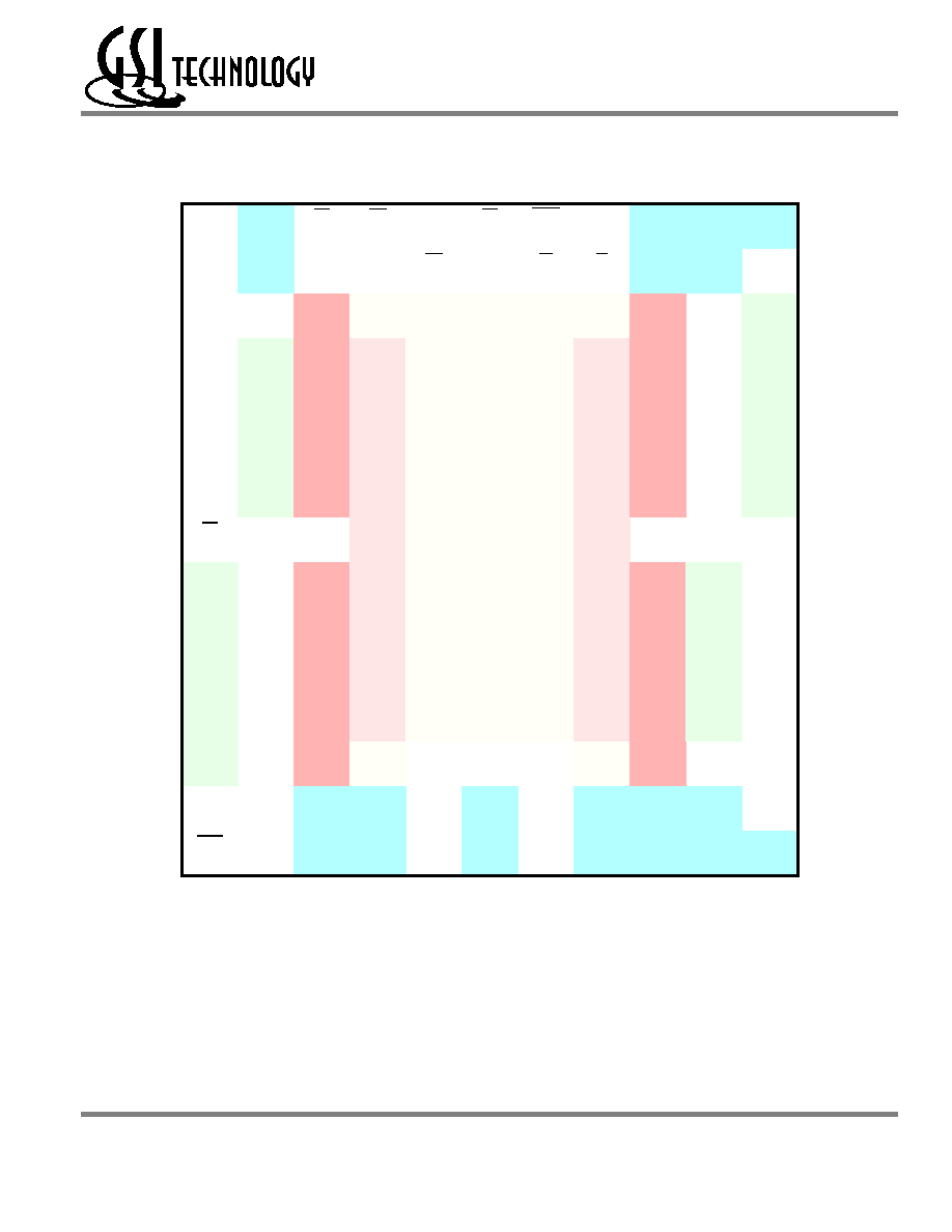
165 Bump BGA--x18 Commom I/O--Top View (Package D)
1
2
3
4
5
6
7
8
9
10
11
A
NC
A
E1
BB
NC
E3
CKE
ADV
A17
A
A19
A
B
NC
A
E2
NC
BA
CK
W
G
A18
A
NC
B
C
NC
NC
V
DDQ
V
SS
V
SS
V
SS
V
SS
V
SS
V
DDQ
NC
DQPA
C
D
NC
DQB
V
DDQ
V
DD
V
SS
V
SS
V
SS
V
DD
V
DDQ
NC
DQA
D
E
NC
DQB
V
DDQ
V
DD
V
SS
V
SS
V
SS
V
DD
V
DDQ
NC
DQA
E
F
NC
DQB
V
DDQ
V
DD
V
SS
V
SS
V
SS
V
DD
V
DDQ
NC
DQA
F
G
NC
DQB
V
DDQ
V
DD
V
SS
V
SS
V
SS
V
DD
V
DDQ
NC
DQA
G
H
FT
MCH
NC
V
DD
V
SS
V
SS
V
SS
V
DD
NC
NC
ZZ
H
J
DQB
NC
V
DDQ
V
DD
V
SS
V
SS
V
SS
V
DD
V
DDQ
DQA
NC
J
K
DQB
NC
V
DDQ
V
DD
V
SS
V
SS
V
SS
V
DD
V
DDQ
DQA
NC
K
L
DQB
NC
V
DDQ
V
DD
V
SS
V
SS
V
SS
V
DD
V
DDQ
DQA
NC
L
M
DQB
NC
V
DDQ
V
DD
V
SS
V
SS
V
SS
V
DD
V
DDQ
DQA
NC
M
N
DQPB
NC
V
DDQ
V
SS
NC
NC
NC
V
SS
V
DDQ
NC
NC
N
P
NC
NC
A
A
TDI
A1
TDO
A
A
A
NC
P
R
LBO
NC
A
A
TMS
A0
TCK
A
A
A
A
R
11 x 15 Bump BGA--13 mm x 15 mm Body--1.0 mm Bump Pitch