
Rev: 1.00a 6/2003
1/36
© 2003, Giga Semiconductor, Inc.
Specifications cited are subject to change without notice. For latest documentation see http://www.gsitechnology.com.
NoBL is a trademark of Cypress Semiconductor Corp.. NtRAM is a trademark of Samsung Electronics Co.. ZBT is a trademark of Integrated Device Technology, Inc.
GS8162ZV18A(B/D)/GS8162ZV36A(B/D)/GS8162ZV72A(C)
18Mb Pipelined and Flow Through
Synchronous NBT SRAM
350 MHz≠150 MHz
1.8 V V
DD
1.8 V I/O
119, 165, & 209 BGA
Commercial Temp
Industrial Temp
Preliminary
Features
∑ NBT (No Bus Turn Around) functionality allows zero wait
Read-Write-Read bus utilization; fully pin-compatible with
both pipelined and flow through NtRAMTM, NoBLTM and
ZBTTM SRAMs
∑ 1.8 V +10%/≠10% core power supply
∑ 1.8 V I/O supply
∑ User-configurable Pipeline and Flow Through mode
∑ ZQ mode pin for user-selectable high/low output drive
∑ IEEE 1149.1 JTAG-compatible Boundary Scan
∑ On-chip write parity checking; even or odd selectable
∑ On-chip parity encoding and error detection
∑ LBO pin for Linear or Interleave Burst mode
∑ Pin-compatible with 2M, 4M, and 8M devices
∑ Byte write operation (9-bit Bytes)
∑ 3 chip enable signals for easy depth expansion
∑ ZZ Pin for automatic power-down
∑ JEDEC-standard 119-, 165-, or 209-Bump BGA package
Functional Description
The GS8162ZV18A(B/D)/V36A(B/D)/V72A(C) is an 18Mbit
Synchronous Static SRAM. GSI's NBT SRAMs, like ZBT,
NtRAM, NoBL or other pipelined read/double late write or
flow through read/single late write SRAMs, allow utilization
of all available bus bandwidth by eliminating the need to insert
deselect cycles when the device is switched from read to write
cycles.
Because it is a synchronous device, address, data inputs, and
read/write control inputs are captured on the rising edge of the
input clock. Burst order control (LBO) must be tied to a power
rail for proper operation. Asynchronous inputs include the
Sleep mode enable (ZZ) and Output Enable. Output Enable can
be used to override the synchronous control of the output
drivers and turn the RAM's output drivers off at any time.
Write cycles are internally self-timed and initiated by the rising
edge of the clock input. This feature eliminates complex off-
chip write pulse generation required by asynchronous SRAMs
and simplifies input signal timing.
The GS8162ZV18A(B/D)/V36A(B/D)/V72A(C) may be
configured by the user to operate in Pipeline or Flow Through
mode. Operating as a pipelined synchronous device, in
addition to the rising-edge-triggered registers that capture input
signals, the device incorporates a rising edge triggered output
register. For read cycles, pipelined SRAM output data is
temporarily stored by the edge-triggered output register during
the access cycle and then released to the output drivers at the
next rising edge of clock.
The GS8162ZV18A(B/D)/V36A(B/D)/V72A(C) is
implemented with GSI's high performance CMOS technology
and is available in a JEDEC-standard 119-bump (x18 & x36),
165-bump (x18 & x36), or 209-bump (x72) BGA package.
Parameter Synopsis
-350
-333
-300
-250
-200
-150
Unit
Pipeline
3-1-1-1
t
KQ
(x18/x36)
t
KQ
(x72)
tCycle
1.8
2.0
2.85
2.0
2.2
3.0
2.2
2.5
3.3
2.3
2.6
4.0
2.7
2.8
5.0
3.3
3.3
6.7
ns
ns
Curr
(x18)
Curr
(x32/x36)
Curr
(x72)
395
455
--
370
430
--
335
390
495
280
330
425
230
270
345
185
210
270
mA
mA
mA
Flow
Through
2-1-1-1
t
KQ
tCycle
4.5
4.5
4.7
4.7
5.0
5.0
5.5
5.5
6.5
6.5
7.5
7.5
ns
ns
Curr
(x18)
Curr
(x32/x36)
Curr
(x72)
270
305
--
250
285
--
230
270
345
210
240
315
185
205
275
170
190
250
mA
mA
mA
Rev: 1.00a 6/2003
2/36
© 2003, Giga Semiconductor, Inc.
Specifications cited are subject to change without notice. For latest documentation see http://www.gsitechnology.com.
GS8162ZV18A(B/D)/GS8162ZV36A(B/D)/GS8162ZV72A(C)
Preliminary
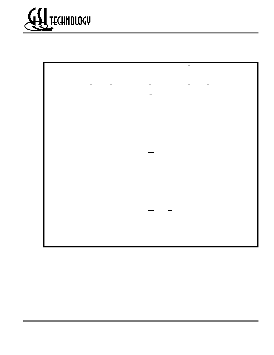
GS8162ZV72 Pad Out
209-Bump BGA--Top View (Package C)
1
2
3
4
5
6
7
8
9
10
11
A DQG5
DQG1
A13
E2
A14
ADV A15
E3
A17
DQB1
DQB5
B DQG6
DQG2
BC
BG
NC
W
A16
BB
BF
DQB2
DQB6
C DQG7
DQG3
BH
BD
NC
E1
NC
BE
BA
DQB3
DQB7
D DQG8
DQG4
V
SS
NC
NC
G
NC
NC
V
SS
DQB4
DQB8
E DQG9
DQC9
V
DDQ
V
DDQ
V
DD
V
DD
V
DD
V
DDQ
V
DDQ
DQF9
DQB9
F
DQC4
DQC8
V
SS
V
SS
V
SS
ZQ
V
SS
V
SS
V
SS
DQF8
DQF4
G DQC3
DQC7
V
DDQ
V
DDQ
V
DD
MCH
V
DD
V
DDQ
V
DDQ
DQF7
DQF3
H DQC2
DQC6
V
SS
V
SS
V
SS
MCL
V
SS
V
SS
V
SS
DQF6
DQF2
J DQC1
DQC5
V
DDQ
V
DDQ
V
DD
MCH
V
DD
V
DDQ
V
DDQ
DQF5
DQF1
K NC
NC
CK
NC
V
SS
CKE
V
SS
NC
NC
NC
NC
L DQH1
DQH5
V
DDQ
V
DDQ
V
DD
FT
V
DD
V
DDQ
V
DDQ
DQA5
DQA1
M DQH2
DQH6
V
SS
V
SS
V
SS
MCL
V
SS
V
SS
V
SS
DQA6
DQA2
N DQH3
DQH7
V
DDQ
V
DDQ
V
DD
MCH
V
DD
V
DDQ
V
DDQ
DQA7
DQA3
P DQH4
DQH8
V
SS
V
SS
V
SS
ZZ
V
SS
V
SS
V
SS
DQA8
DQA4
R DQD9
DQH9
V
DDQ
V
DDQ
V
DD
V
DD
V
DD
V
DDQ
V
DDQ
DQA9
DQE9
T DQD8
DQD4
V
SS
NC
NC
LBO
PE
NC
V
SS
DQE4
DQE8
U DQD7
DQD3
NC
A12
NC
A11
NC
A10
NC
DQE3
DQE7
V
DQD6
DQD2
A9
A8
A7
A1
A6
A5
A4
DQE2
DQE6
W
DQD5
DQD1
TMS
TDI
A3
A0
A2
TDO
TCK
DQE1
DQE5
Rev 10
11 x 19 Bump BGA--14 x 22 mm
2
Body--1 mm Bump Pitch
Rev: 1.00a 6/2003
3/36
© 2003, Giga Semiconductor, Inc.
Specifications cited are subject to change without notice. For latest documentation see http://www.gsitechnology.com.
GS8162ZV18A(B/D)/GS8162ZV36A(B/D)/GS8162ZV72A(C)
Preliminary
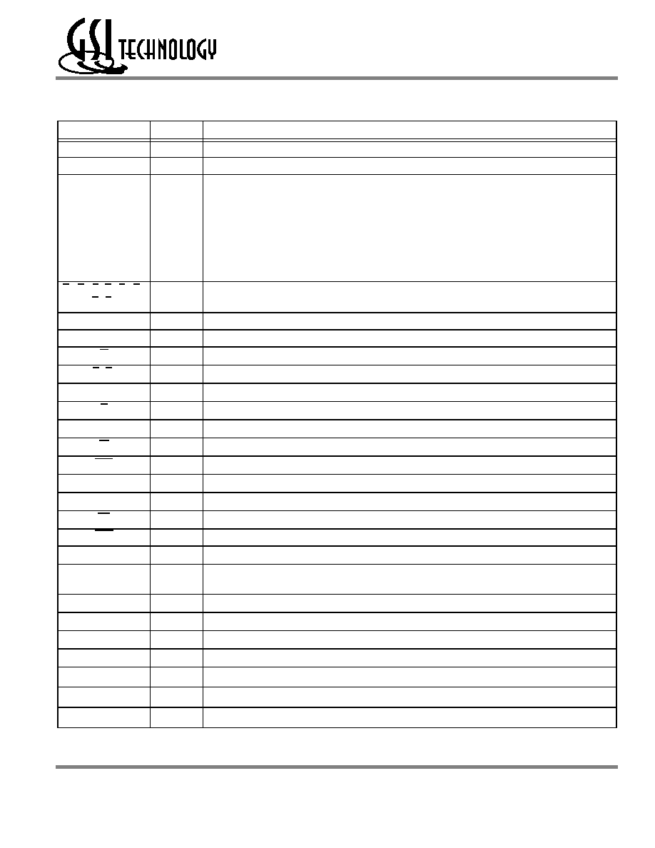
GS8162ZV72 BGA Pin Description
Symbol
Type
Description
A
0
, A
1
I
Address field LSBs and Address Counter Preset Inputs
An
I
Address Inputs
DQ
A1
≠DQ
A9
DQ
B1
≠DQ
B9
DQ
C1
≠DQ
C9
DQ
D1
≠DQ
D9
DQ
E1
≠DQ
E9
DQ
F1
≠DQ
F9
DQ
G1
≠DQ
G9
DQ
H1
≠DQ
H9
I/O
Data Input and Output pins
B
A
, B
B
, B
C
,B
D,
B
E
, B
F
,
B
G
,B
H
I
Byte Write Enable for DQ
A
, DQ
B
, DQ
C
, DQ
D,
DQ
E
,
DQ
F
, DQ
G
, DQ
H
I/Os; active low
NC
--
No Connect
CK
I
Clock Input Signal; active high
W
I
Write Enable. Writes all enabled bytes; active low
E
1,
E
3
I
Chip Enable; active low
E
2
I
Chip Enable; active high
G
I
Output Enable; active low
ZZ
I
Sleep Mode control; active high
FT
I
Flow Through or Pipeline mode; active low
LBO
I
Linear Burst Order mode; active low
MCH
I
Must Connect High
MCL
Must Connect Low
PE
I
Parity Bit Enable; active low (High = x16/32 Mode, Low = x18/36 Mode)
CKE
I
Clock Enable; active low
ADV
I
Burst Address Counter Advance Enable; active high
ZQ
I
FLXDrive Output Impedance Control
(Low = Low Impedance [High Drive], High = High Impedance [Low Drive])
TMS
I
Scan Test Mode Select
TDI
I
Scan Test Data In
TDO
O
Scan Test Data Out
TCK
I
Scan Test Clock
V
DD
I
Core power supply
V
SS
I
I/O and Core Ground
V
DDQ
I
Output driver power supply

Rev: 1.00a 6/2003
4/36
© 2003, Giga Semiconductor, Inc.
Specifications cited are subject to change without notice. For latest documentation see http://www.gsitechnology.com.
GS8162ZV18A(B/D)/GS8162ZV36A(B/D)/GS8162ZV72A(C)
Preliminary
165 Bump BGA--x18 Commom I/O--Top View (Package D)
1
2
3
4
5
6
7
8
9
10
11
A
NC
A6
E1
BB
NC
E3
CKE
ADV
A17
A8
A19
A
B
NC
A7
E2
NC
BA
CK
W
G
A18
A9
NC
B
C
NC
NC
V
DDQ
V
SS
V
SS
V
SS
V
SS
V
SS
V
DDQ
NC
DQA
C
D
NC
DQB
V
DDQ
V
DD
V
SS
V
SS
V
SS
V
DD
V
DDQ
NC
DQA
D
E
NC
DQB
V
DDQ
V
DD
V
SS
V
SS
V
SS
V
DD
V
DDQ
NC
DQA
E
F
NC
DQB
V
DDQ
V
DD
V
SS
V
SS
V
SS
V
DD
V
DDQ
NC
DQA
F
G
NC
DQB
V
DDQ
V
DD
V
SS
V
SS
V
SS
V
DD
V
DDQ
NC
DQA
G
H
FT
MCH
NC
V
DD
V
SS
V
SS
V
SS
V
DD
NC
ZQ
ZZ
H
J
DQB
NC
V
DDQ
V
DD
V
SS
V
SS
V
SS
V
DD
V
DDQ
DQA
NC
J
K
DQB
NC
V
DDQ
V
DD
V
SS
V
SS
V
SS
V
DD
V
DDQ
DQA
NC
K
L
DQB
NC
V
DDQ
V
DD
V
SS
V
SS
V
SS
V
DD
V
DDQ
DQA
NC
L
M
DQB
NC
V
DDQ
V
DD
V
SS
V
SS
V
SS
V
DD
V
DDQ
DQA
NC
M
N
DQB
DNU
V
DDQ
V
SS
NC
NC
NC
V
SS
V
DDQ
NC
NC
N
P
NC
NC
A5
A4
TDI
A1
TDO
A11
A12
A14
NC
P
R
LBO
NC
A3
A2
TMS
A0
TCK
A10
A13
A15
A16
R
11 x 15 Bump BGA--13 mm x 15 mm Body--1.0 mm Bump Pitch

Rev: 1.00a 6/2003
5/36
© 2003, Giga Semiconductor, Inc.
Specifications cited are subject to change without notice. For latest documentation see http://www.gsitechnology.com.
GS8162ZV18A(B/D)/GS8162ZV36A(B/D)/GS8162ZV72A(C)
Preliminary
165 Bump BGA--x36 Common I/O--Top View (Package D)
1
2
3
4
5
6
7
8
9
10
11
A
NC
A6
E1
BC
BB
E3
CKE
ADV
A17
A8
NC
A
B
NC
A7
E2
BD
BA
CK
W
G
A18
A9
NC
B
C
DQC
NC
V
DDQ
V
SS
V
SS
V
SS
V
SS
V
SS
V
DDQ
NC
DQB
C
D
DQC
DQC
V
DDQ
V
DD
V
SS
V
SS
V
SS
V
DD
V
DDQ
DQB
DQB
D
E
DQC
DQC
V
DDQ
V
DD
V
SS
V
SS
V
SS
V
DD
V
DDQ
DQB
DQB
E
F
DQC
DQC
V
DDQ
V
DD
V
SS
V
SS
V
SS
V
DD
V
DDQ
DQB
DQB
F
G
DQC
DQC
V
DDQ
V
DD
V
SS
V
SS
V
SS
V
DD
V
DDQ
DQB
DQB
G
H
FT
MCH
NC
V
DD
V
SS
V
SS
V
SS
V
DD
NC
ZQ
ZZ
H
J
DQD
DQD
V
DDQ
V
DD
V
SS
V
SS
V
SS
V
DD
V
DDQ
DQA
DQA
J
K
DQD
DQD
V
DDQ
V
DD
V
SS
V
SS
V
SS
V
DD
V
DDQ
DQA
DQA
K
L
DQD
DQD
V
DDQ
V
DD
V
SS
V
SS
V
SS
V
DD
V
DDQ
DQA
DQA
L
M
DQD
DQD
V
DDQ
V
DD
V
SS
V
SS
V
SS
V
DD
V
DDQ
DQA
DQA
M
N
DQD
DNU
V
DDQ
V
SS
NC
NC
NC
V
SS
V
DDQ
NC
DQA
N
P
NC
NC
A5
A4
TDI
A1
TDO
A11
A12
A14
NC
P
R
LBO
NC
A3
A2
TMS
A0
TCK
A10
A13
A15
A16
R
11 x 15 Bump BGA--13 mm x 15 mm Body--1.0 mm Bump Pitch
Rev: 1.00a 6/2003
6/36
© 2003, Giga Semiconductor, Inc.
Specifications cited are subject to change without notice. For latest documentation see http://www.gsitechnology.com.
GS8162ZV18A(B/D)/GS8162ZV36A(B/D)/GS8162ZV72A(C)
Preliminary
GS8162ZV36 Pad Out
119 Bump BGA--Top View (Package B)
1
2
3
4
5
6
7
A
V
DDQ
A
6
A
7
A
18
A
8
A
9
V
DDQ
B
NC
E
2
A
4
ADV
A
15
E
3
NC
C
NC
A
5
A
3
V
DD
A
14
A
16
NC
D
DQ
C4
DQ
C9
V
SS
ZQ
V
SS
DQ
B9
DQ
B4
E
DQ
C3
DQ
C8
V
SS
E
1
V
SS
DQ
B8
DQ
B3
F
V
DDQ
DQ
C7
V
SS
G
V
SS
DQ
B7
V
DDQ
G
DQ
C2
DQ
C6
B
C
A
17
B
B
DQ
B6
DQ
B2
H
DQ
C1
DQ
C5
V
SS
W
V
SS
DQ
B5
DQ
B1
J
V
DDQ
V
DD
NC
V
DD
NC
V
DD
V
DDQ
K
DQ
A1
DQ
A5
V
SS
CK
V
SS
DQ
A5
DQ
A1
L
DQ
A2
DQ
A6
B
D
NC
B
A
DQ
A6
DQ
A2
M
V
DDQ
DQ
A7
V
SS
CKE
V
SS
DQ
A7
V
DDQ
N
DQ
A3
DQ
A8
V
SS
A
1
V
SS
DQ
A8
DQ
A3
P
DQ
A4
DQ
A9
V
SS
A
0
V
SS
DQ
A9
DQ
A4
R
NC
A
2
LBO
V
DD
FT
A
13
PE
T
NC
NC
A
10
A
11
A
12
NC
ZZ
U
V
DDQ
TMS
TDI
TCK
TDO
NC
V
DDQ
Rev: 1.00a 6/2003
7/36
© 2003, Giga Semiconductor, Inc.
Specifications cited are subject to change without notice. For latest documentation see http://www.gsitechnology.com.
GS8162ZV18A(B/D)/GS8162ZV36A(B/D)/GS8162ZV72A(C)
Preliminary
GS8162ZV18A Pad Out
119 Bump BGA--Top View (Package B)
1
2
3
4
5
6
7
A
V
DDQ
A
6
A
7
A
18
A
8
A
9
V
DDQ
B
NC
E
2
A
4
ADV
A
15
E
3
NC
C
NC
A
5
A
3
V
DD
A
14
A
16
NC
D
DQ
B1
NC
V
SS
ZQ
V
SS
DQ
PA9
NC
E
NC
DQ
B2
V
SS
E
1
V
SS
NC
DQ
A8
F
V
DDQ
NC
V
SS
G
V
SS
DQ
A7
V
DDQ
G
NC
DQ
B3
B
B
A
17
NC
NC
DQ
A6
H
DQ
B4
NC
V
SS
W
V
SS
DQ
A5
NC
J
V
DDQ
V
DD
NC
V
DD
NC
V
DD
V
DDQ
K
NC
DQ
B5
V
SS
CK
V
SS
NC
DQ
A4
L
DQ
B6
NC
NC
NC
B
A
DQ
A3
NC
M
V
DDQ
DQ
B7
V
SS
CKE
V
SS
NC
V
DDQ
N
DQ
B8
NC
V
SS
A
1
V
SS
DQ
A2
NC
P
NC
DQ
PB9
V
SS
A
0
V
SS
NC
DQ
A1
R
NC
A
2
LBO
V
DD
FT
A
13
PE
T
NC
A
10
A
11
NC
A
12
A
19
ZZ
U
V
DDQ
TMS
TDI
TCK
TDO
NC
V
DDQ
Rev: 1.00a 6/2003
8/36
© 2003, Giga Semiconductor, Inc.
Specifications cited are subject to change without notice. For latest documentation see http://www.gsitechnology.com.
GS8162ZV18A(B/D)/GS8162ZV36A(B/D)/GS8162ZV72A(C)
Preliminary
BPR1999.05.18
GS8162ZV18/36 119-Bump and 165-Bump BGA Pin Description
Symbol
Type
Description
A
0
, A
1
I
Address field LSBs and Address Counter Preset Inputs
An
I
Address Inputs
DQ
A1
≠DQ
A9
DQ
B1
≠DQ
B9
DQ
C1
≠DQ
C0
DQ
D1
≠DQ
D0
I/O
Data Input and Output pins
B
A
, B
B
, B
C
, B
D
I
Byte Write Enable for DQ
A
, DQ
B
, DQ
C
, DQ
D
I/Os; active low
NC
--
No Connect
CK
I
Clock Input Signal; active high
CKE
I
Clock Enable; active low
PE
I
Parity Bit Enable; active low (High = x16/32 Mode, Low = x18/36 Mode)
W
I
Write Enable; active low
E
1
I
Chip Enable; active low
E
3
I
Chip Enable; active low
E
2
I
Chip Enable; active high
G
I
Output Enable; active low
ADV
I
Burst address counter advance enable; active high
ZZ
I
Sleep mode control; active high
FT
I
Flow Through or Pipeline mode; active low
LBO
I
Linear Burst Order mode; active low
ZQ
I
FLXDrive Output Impedance Control (Low = Low Impedance [High Drive], High = High Impedance [Low
Drive])
TMS
I
Scan Test Mode Select
TDI
I
Scan Test Data In
TDO
O
Scan Test Data Out
TCK
I
Scan Test Clock
V
DD
I
Core power supply
V
SS
I
I/O and Core Ground
V
DDQ
I
Output driver power supply
Rev: 1.00a 6/2003
9/36
© 2003, Giga Semiconductor, Inc.
Specifications cited are subject to change without notice. For latest documentation see http://www.gsitechnology.com.
GS8162ZV18A(B/D)/GS8162ZV36A(B/D)/GS8162ZV72A(C)
Preliminary
Functional Details
Clocking
Deassertion of the Clock Enable (CKE) input blocks the Clock input from reaching the RAM's internal circuits. It may be used to
suspend RAM operations. Failure to observe Clock Enable set-up or hold requirements will result in erratic operation.
Pipeline Mode Read and Write Operations
All inputs (with the exception of Output Enable, Linear Burst Order and Sleep) are synchronized to rising clock edges. Single cycle
read and write operations must be initiated with the Advance/Load pin (ADV) held low, in order to load the new address. Device
activation is accomplished by asserting all three of the Chip Enable inputs (E
1
, E
2,
and E
3
). Deassertion of any one of the Enable
inputs will deactivate the device.
Read operation is initiated when the following conditions are satisfied at the rising edge of clock: CKE is asserted low, all three
chip enables (E
1
, E
2,
and E
3
) are active, the write enable input signals W is deasserted high, and ADV is asserted low. The address
presented to the address inputs is latched into the address register and presented to the memory core and control logic. The control
logic determines that a read access is in progress and allows the requested data to propagate to the input of the output register. At
the next rising edge of clock the read data is allowed to propagate through the output register and onto the output pins.
Write operation occurs when the RAM is selected, CKE is active, and the Write input is sampled low at the rising edge of clock.
The Byte Write Enable inputs (B
A
, B
B
, B
C,
and B
D
) determine which bytes will be written. All or none may be activated. A write
cycle with no Byte Write inputs active is a no-op cycle. The pipelined NBT SRAM provides double late write functionality,
matching the write command versus data pipeline length (2 cycles) to the read command versus data pipeline length (2 cycles). At
the first rising edge of clock, Enable, Write, Byte Write(s), and Address are registered. The Data In associated with that address is
required at the third rising edge of clock.
Flow Through Mode Read and Write Operations
Operation of the RAM in Flow Through mode is very similar to operations in Pipeline mode. Activation of a Read Cycle and the
use of the Burst Address Counter is identical. In Flow Through mode the device may begin driving out new data immediately after
new address are clocked into the RAM, rather than holding new data until the following (second) clock edge. Therefore, in Flow
Through mode the read pipeline is one cycle shorter than in Pipeline mode.
Write operations are initiated in the same way, but differ in that the write pipeline is one cycle shorter as well, preserving the ability
to turn the bus from reads to writes without inserting any dead cycles. While the pipelined NBT RAMs implement a double late
write protocol in Flow Through mode a single late write protocol mode is observed. Therefore, in Flow Through mode, address
and control are registered on the first rising edge of clock and data in is required at the data input pins at the second rising edge of
clock.
Function
W
B
A
B
B
B
C
B
D
Read
H
X
X
X
X
Write Byte "a"
L
L
H
H
H
Write Byte "b"
L
H
L
H
H
Write Byte "c"
L
H
H
L
H
Write Byte "d"
L
H
H
H
L
Write all Bytes
L
L
L
L
L
Write Abort/NOP
L
H
H
H
H

Rev: 1.00a 6/2003
10/36
© 2003, Giga Semiconductor, Inc.
Specifications cited are subject to change without notice. For latest documentation see http://www.gsitechnology.com.
GS8162ZV18A(B/D)/GS8162ZV36A(B/D)/GS8162ZV72A(C)
Preliminary
Synchronous Truth Table
Operation
Type Address E
1
E
2
E
3
ZZ ADV W Bx G CKE CK
DQ
Notes
Deselect Cycle, Power Down
D
None
H
X
X
L
L
X
X
X
L
L-H High-Z
Deselect Cycle, Power Down
D
None
X
X
H
L
L
X
X
X
L
L-H High-Z
Deselect Cycle, Power Down
D
None
X
L
X
L
L
X
X
X
L
L-H High-Z
Deselect Cycle, Continue
D
None
X
X
X
L
H
X
X
X
L
L-H High-Z
1
Read Cycle, Begin Burst
R
External
L
H
L
L
L
H
X
L
L
L-H
Q
Read Cycle, Continue Burst
B
Next
X
X
X
L
H
X
X
L
L
L-H
Q
1,10
NOP/Read, Begin Burst
R
External
L
H
L
L
L
H
X
H
L
L-H High-Z
2
Dummy Read, Continue Burst
B
Next
X
X
X
L
H
X
X
H
L
L-H High-Z
1,2,10
Write Cycle, Begin Burst
W
External
L
H
L
L
L
L
L
X
L
L-H
D
3
Write Cycle, Continue Burst
B
Next
X
X
X
L
H
X
L
X
L
L-H
D
1,3,10
NOP/Write Abort, Begin Burst
W
None
L
H
L
L
L
L
H
X
L
L-H High-Z
2,3
Write Abort, Continue Burst
B
Next
X
X
X
L
H
X
H
X
L
L-H High-Z 1,2,3,10
Clock Edge Ignore, Stall
Current
X
X
X
L
X
X
X
X
H
L-H
-
4
Sleep Mode
None
X
X
X
H
X
X
X
X
X
X
High-Z
Notes:
1. Continue Burst cycles, whether Read or Write, use the same control inputs. A Deselect continue cycle can only be entered into if a
Deselect cycle is executed first.
2. Dummy Read and Write abort can be considered NOPs because the SRAM performs no operation. A Write abort occurs when the W pin
is sampled low but no Byte Write pins are active, so no write operation is performed.
3. G can be wired low to minimize the number of control signals provided to the SRAM. Output drivers will automatically turn off during write
cycles.
4. If CKE High occurs during a pipelined read cycle, the DQ bus will remain active (Low Z). If CKE High occurs during a write cycle, the bus
will remain in High Z.
5. X = Don't Care; H = Logic High; L = Logic Low; Bx = High = All Byte Write signals are high; Bx = Low = One or more Byte/Write signals
are Low
6. All inputs, except G and ZZ must meet setup and hold times of rising clock edge.
7. Wait states can be inserted by setting CKE high.
8. This device contains circuitry that ensures all outputs are in High Z during power-up.
9. A 2-bit burst counter is incorporated.
10. The address counter is incriminated for all Burst continue cycles.

Rev: 1.00a 6/2003
11/36
© 2003, Giga Semiconductor, Inc.
Specifications cited are subject to change without notice. For latest documentation see http://www.gsitechnology.com.
GS8162ZV18A(B/D)/GS8162ZV36A(B/D)/GS8162ZV72A(C)
Preliminary
Deselect
New Read
New Write
Burst Read
Burst Write
W
R
B
R
B
W
D
D
B
B
W
R
D
B
W
R
D
D
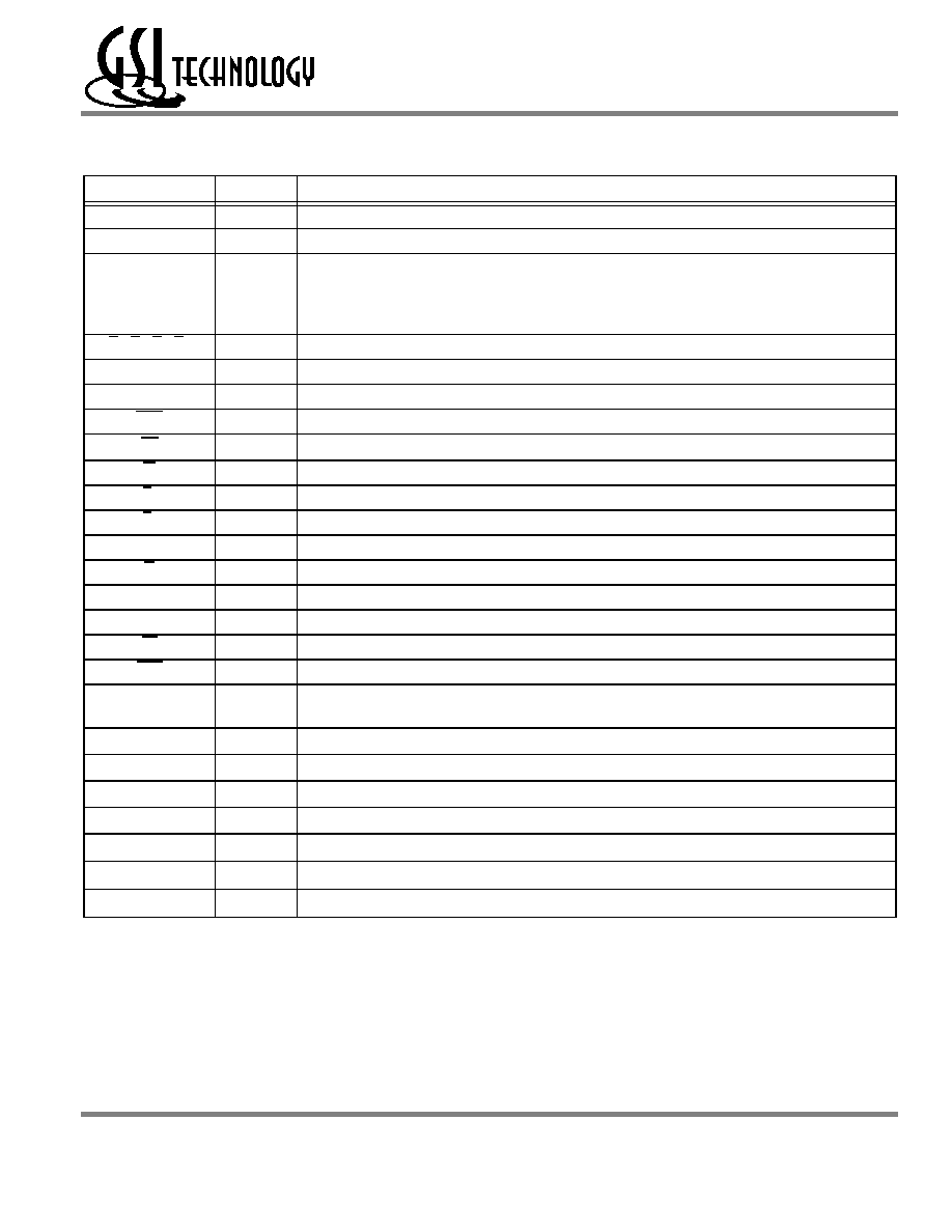
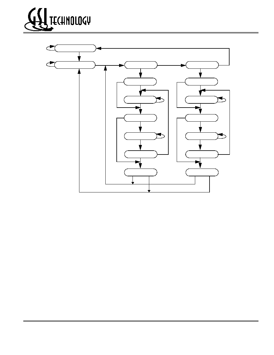
Pipelined and Flow Through Read Write Control State Diagram
Current State (n)
Next State (n+1)
Transition
Input Command Code
Key
Notes
1. The Hold command (CKE Low) is not
shown because it prevents any state change.
2. W, R, B, and D represent input command
codes as indicated in the Synchronous Truth Table.
Clock (CK)
Command
Current State
Next State
n
n+1
n+2
n+3
Current State and Next State Definition for
Pipelined and Flow through Read/Write Control State Diagram
W
R
Rev: 1.00a 6/2003
12/36
© 2003, Giga Semiconductor, Inc.
Specifications cited are subject to change without notice. For latest documentation see http://www.gsitechnology.com.
GS8162ZV18A(B/D)/GS8162ZV36A(B/D)/GS8162ZV72A(C)
Preliminary
Intermediate
Intermediate
Intermediate
Intermediate
Intermediate
Intermediate
High Z
(Data In)
Data Out
(Q Valid)
High Z
B W
B
R
B
D
R
W
R
W
D
D
Pipeline Mode Data I/O State Diagram
Current State (n)
Next State (n+2)
Transition
Input Command Code
Key
Transition
Intermediate State (N+1)
Notes
1. The Hold command (CKE Low) is not
shown because it prevents any state change.
2. W, R, B, and D represent input command
codes as indicated in the Truth Tables.
Clock (CK)
Command
Current State
Intermediate
n
n+1
n+2
n+3
Current State and Next State Definition for
Pipeline Mode Data I/O State Diagram
Next State
State
Rev: 1.00a 6/2003
13/36
© 2003, Giga Semiconductor, Inc.
Specifications cited are subject to change without notice. For latest documentation see http://www.gsitechnology.com.
GS8162ZV18A(B/D)/GS8162ZV36A(B/D)/GS8162ZV72A(C)
Preliminary
High Z
(Data In)
Data Out
(Q Valid)
High Z
B W
B
R
B
D
R
W
R
W
D
D
Current State (n)
Next State (n+1)
Transition
Input Command Code
Key
Notes
1. The Hold command (CKE Low) is not
shown because it prevents any state change.
2. W, R, B, and D represent input command
codes as indicated in the Truth Tables.
Flow Through Mode Data I/O State Diagram
Clock (CK)
Command
Current State
Next State
n
n+1
n+2
n+3
Current State and Next State Definition for:
Pipeline and Flow Through Read Write Control State Diagram
Rev: 1.00a 6/2003
14/36
© 2003, Giga Semiconductor, Inc.
Specifications cited are subject to change without notice. For latest documentation see http://www.gsitechnology.com.
GS8162ZV18A(B/D)/GS8162ZV36A(B/D)/GS8162ZV72A(C)
Preliminary
Burst Cycles
Although NBT RAMs are designed to sustain 100% bus bandwidth by eliminating turnaround cycle when there is transition from
read to write, multiple back-to-back reads or writes may also be performed. NBT SRAMs provide an on-chip burst address
generator that can be utilized, if desired, to further simplify burst read or write implementations. The ADV control pin, when
driven high, commands the SRAM to advance the internal address counter and use the counter generated address to read or write
the SRAM. The starting address for the first cycle in a burst cycle series is loaded into the SRAM by driving the ADV pin low, into
Load mode.
Burst Order
The burst address counter wraps around to its initial state after four addresses (the loaded address and three more) have been
accessed. The burst sequence is determined by the state of the Linear Burst Order pin (LBO). When this pin is Low, a linear burst
sequence is selected. When the RAM is installed with the LBO pin tied high, Interleaved burst sequence is selected. See the tables
below for details.
FLXDriveTM
The ZQ pin allows selection between NBT RAM nominal drive strength (ZQ low) for multi-drop bus applications and low drive
strength (ZQ floating or high) point-to-point applications. See the Output Driver Characteristics chart for details.
Note:
There arepull-up devices on the ZQ, SCD, and FT pins and pull-down device on the ZZ pin, so those input pins can be unconnected and the chip
will operate in the default states as specified in the above tables.
Enable / Disable Parity I/O Pins
This SRAM allows the user to configure the device to operate in Parity I/O active (x18, x36, or x72) or in Parity I/O inactive (x16,
x32, or x64) mode. Holding the PE bump low or letting it float will activate the 9th I/O on each byte of the RAM.
Mode Pin Functions
Mode Name
Pin
Name
State
Function
Burst Order Control
LBO
L
Linear Burst
H
Interleaved Burst
Output Register Control
FT
L
Flow Through
H or NC
Pipeline
Power Down Control
ZZ
L or NC
Active
H
Standby, I
DD
= I
SB
FLXDrive Output Impedance Control
ZQ
L
High Drive (Low Impedance)
H or NC
Low Drive (High Impedance)
9th I/O Enable
PE
L or NC
Activate 9th I/Os
H
Deactivate 9th I/Os
Rev: 1.00a 6/2003
15/36
© 2003, Giga Semiconductor, Inc.
Specifications cited are subject to change without notice. For latest documentation see http://www.gsitechnology.com.
GS8162ZV18A(B/D)/GS8162ZV36A(B/D)/GS8162ZV72A(C)
Preliminary
Burst Counter Sequences
BPR 1999.05.18
Sleep Mode
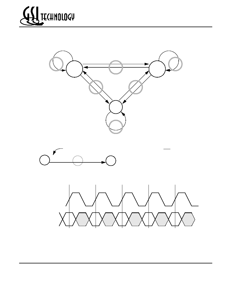
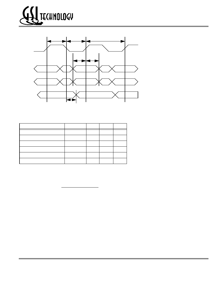
During normal operation, ZZ must be pulled low, either by the user or by its internal pull down resistor. When ZZ is pulled high,
the SRAM will enter a Power Sleep mode after 2 cycles. At this time, internal state of the SRAM is preserved. When ZZ returns to
low, the SRAM operates normally after ZZ recovery time.
Sleep mode is a low current, power-down mode in which the device is deselected and current is reduced to I
SB
2. The duration of
Sleep mode is dictated by the length of time the ZZ is in a High state. After entering Sleep mode, all inputs except ZZ become
disabled and all outputs go to High-Z The ZZ pin is an asynchronous, active high input that causes the device to enter Sleep mode.
When the ZZ pin is driven high, I
SB
2 is guaranteed after the time tZZI is met. Because ZZ is an asynchronous input, pending
operations or operations in progress may not be properly completed if ZZ is asserted. Therefore, Sleep mode must not be initiated
until valid pending operations are completed. Similarly, when exiting Sleep mode during tZZR, only a Deselect or Read commands
may be applied while the SRAM is recovering from Sleep mode.
Sleep Mode Timing Diagram
Designing for Compatibility
The GSI NBT SRAMs offer users a configurable selection between Flow Through mode and Pipeline mode via the FT signal found
on Bump 5R. Not all vendors offer this option, however most mark Bump 5R as V
DD
or V
DDQ
on pipelined parts and V
SS
on flow
through parts. GSI NBT SRAMs are fully compatible with these sockets.
Linear Burst Sequence
Note: The burst counter wraps to initial state on the 5th clock.
I
nterleaved Burst Sequence
Note: The burst counter wraps to initial state on the 5th clock.
A[1:0] A[1:0] A[1:0] A[1:0]
1st address
00
01
10
11
2nd address
01
10
11
00
3rd address
10
11
00
01
4th address
11
00
01
10
A[1:0] A[1:0] A[1:0] A[1:0]
1st address
00
01
10
11
2nd address
01
00
11
10
3rd address
10
11
00
01
4th address
11
10
01
00
CK
ZZ
tZZR
tZZH
tZZS
~ ~
~ ~
Sleep
~ ~
~ ~
~ ~
Rev: 1.00a 6/2003
16/36
© 2003, Giga Semiconductor, Inc.
Specifications cited are subject to change without notice. For latest documentation see http://www.gsitechnology.com.
GS8162ZV18A(B/D)/GS8162ZV36A(B/D)/GS8162ZV72A(C)
Preliminary
Note:
Permanent damage to the device may occur if the Absolute Maximum Ratings are exceeded. Operation should be restricted to Recommended
Operating Conditions. Exposure to conditions exceeding the Absolute Maximum Ratings, for an extended period of time, may affect reliability of
this component.
Absolute Maximum Ratings
(All voltages reference to V
SS
)
Symbol
Description
Value
Unit
V
DD
Voltage on V
DD
Pins
≠0.5 to 3.6
V
V
DDQ
Voltage in V
DDQ
Pins
≠0.5 to 3.6
V
V
I/O
Voltage on I/O Pins
≠0.5 to V
DDQ
+0.5 (
3.6 V max.)
V
V
IN
Voltage on Other Input Pins
≠0.5 to V
DD
+0.5 (
3.6 V max.)
V
I
IN
Input Current on Any Pin
+/≠20
mA
I
OUT
Output Current on Any I/O Pin
+/≠20
mA
P
D
Package Power Dissipation
1.5
W
T
STG
Storage Temperature
≠55 to 125
o
C
T
BIAS
Temperature Under Bias
≠55 to 125
o
C
Rev: 1.00a 6/2003
17/36
© 2003, Giga Semiconductor, Inc.
Specifications cited are subject to change without notice. For latest documentation see http://www.gsitechnology.com.
GS8162ZV18A(B/D)/GS8162ZV36A(B/D)/GS8162ZV72A(C)
Preliminary
Power Supply Voltage Ranges
Parameter
Symbol
Min.
Typ.
Max.
Unit
Notes
1.8 V Supply Voltage
V
DD1
1.6
1.8
2.0
V
1.8 V V
DDQ
I/O Supply Voltage
V
DDQ1
1.6
1.8
2.0
V
Notes:
1.
The part numbers of Industrial Temperature Range versions end the character "I". Unless otherwise noted, all performance specifications quoted are
evaluated for worst case in the temperature range marked on the device.
2.
Input Under/overshoot voltage must be ≠2 V > Vi < V
DDn
+2 V not to exceed 3.6 V maximum, with a pulse width not to exceed 20% tKC.
V
DDQ
Range Logic Levels
Parameter
Symbol
Min.
Typ.
Max.
Unit
Notes
V
DD
Input High Voltage
V
IH
0.6*V
DD
--
V
DD
+ 0.3
V
1
V
DD
Input Low Voltage
V
IL
≠0.3
--
0.3*V
DD
V
1
V
DDQ
I/O Input High Voltage
V
IHQ
0.6*V
DD
--
V
DDQ
+ 0.3
V
1,3
V
DDQ
I/O Input Low Voltage
V
ILQ
≠0.3
--
0.3*V
DD
V
1,3
Notes:
1.
The part numbers of Industrial Temperature Range versions end the character "I". Unless otherwise noted, all performance specifications quoted are
evaluated for worst case in the temperature range marked on the device.
2.
Input Under/overshoot voltage must be ≠2 V > Vi < V
DDn
+2 V not to exceed 3.6 V maximum, with a pulse width not to exceed 20% tKC.
3.
V
IHQ
(max) is voltage on V
DDQ
pins plus 0.3 V.
Recommended Operating Temperatures
Parameter
Symbol
Min.
Typ.
Max.
Unit
Notes
Ambient Temperature (Commercial Range Versions)
T
A
0
25
70
∞
C
2
Ambient Temperature (Industrial Range Versions)
T
A
≠40
25
85
∞
C
2
Note:
1.
The part numbers of Industrial Temperature Range versions end the character "I". Unless otherwise noted, all performance specifications quoted are
evaluated for worst case in the temperature range marked on the device.
2.
Input Under/overshoot voltage must be ≠2 V > Vi < V
DDn
+2 V not to exceed 3.6 V maximum, with a pulse width not to exceed 20% tKC.
Rev: 1.00a 6/2003
18/36
© 2003, Giga Semiconductor, Inc.
Specifications cited are subject to change without notice. For latest documentation see http://www.gsitechnology.com.
GS8162ZV18A(B/D)/GS8162ZV36A(B/D)/GS8162ZV72A(C)
Preliminary
Note: These parameters are sample tested.
Capacitance
(T
A
= 25
o
C, f = 1 MH
Z
, V
DD
= 2.5 V)
Parameter
Symbol
Test conditions
Typ.
Max.
Unit
Input Capacitance
C
IN
V
IN
= 0 V
4
5
pF
Input/Output Capacitance
C
I/O
V
OUT
= 0 V
6
7
pF
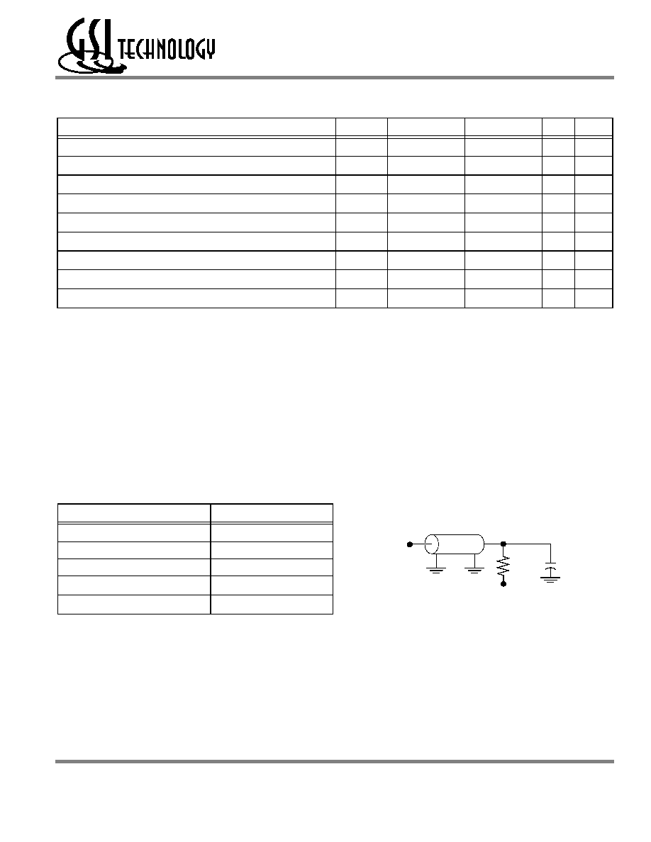
AC Test Conditions
Parameter
Conditions
Input high level
V
DD
≠ 0.2 V
Input low level
0.2 V
Input slew rate
1 V/ns
Input reference level
V
DD
/2
Output reference level
V
DDQ
/2
Output load
Fig. 1
Notes:
1. Include scope and jig capacitance.
2. Test conditions as specified with output loading as shown in Fig. 1
unless otherwise noted.
3. Device is deselected as defined by the Truth Table.
20% tKC
V
SS
≠ 2.0 V
50%
V
SS
V
IH
Undershoot Measurement and Timing
Overshoot Measurement and Timing
20% tKC
V
DD
+ 2.0 V
50%
V
DD
V
IL
DQ
V
DDQ/2
50
30pF
*
Output Load 1
* Distributed Test Jig Capacitance
Rev: 1.00a 6/2003
19/36
© 2003, Giga Semiconductor, Inc.
Specifications cited are subject to change without notice. For latest documentation see http://www.gsitechnology.com.
GS8162ZV18A(B/D)/GS8162ZV36A(B/D)/GS8162ZV72A(C)
Preliminary
DC Electrical Characteristics
Parameter
Symbol
Test Conditions
Min
Max
Input Leakage Current
(except mode pins)
I
IL
V
IN
= 0 to V
DD
≠1 uA
1 uA
ZZ and PE Input Current
I
IN1
V
DD
V
IN
V
IH
0 V
V
IN
V
IH
≠1 uA
≠1 uA
1 uA
100 uA
FT, ZQ Input Current
I
IN2
V
DD
V
IN
V
IL
0 V
V
IN
V
IL
≠100 uA
≠1 uA
1 uA
1 uA
Output Leakage Current
I
OL
Output Disable, V
OUT
= 0 to V
DD
≠1 uA
1 uA
Output High Voltage
V
OH
I
OH
= ≠4 mA, V
DDQ
= 1.6 V
V
DDQ
≠ 0.4 V
--
Output Low Voltage
V
OL
I
OL
= 4 mA, V
DD
= 1.6 V
--
0.4 V
Rev: 1.00a 6/2003
20/36
© 2003, Giga Semiconductor, Inc.
Specifications cited are subject to change without notice. For latest documentation see http://www.gsitechnology.com.
GS8162ZV18A(B/D)/GS8162ZV36A(B/D)/GS8162ZV72A(C)
Preliminary
Operating Currents
Notes:
1.
I
DD
an
d I
DDQ
apply to any combination of V
DD3
, V
DD2
, V
DD
Q
3
, and V
DDQ2
operation.
2.
All p
a
rameters listed are worst case scenario.
Parameter
T
est Conditions
Mode
Symbol
-350
-333
-300
-250
-
2
00
-
1
50
Uni
t
0
to
70
∞C
≠
40
to
85
∞C
0
to
70
∞C
≠
40
to
85
∞C
0
to
70
∞C
≠
40
to
85
∞C
0
to
70
∞C
≠
40
to
85
∞C
0
to
70
∞C
≠
40
to
85
∞C
0
to
70
∞C
≠
40
to
85
∞C
O
p
er
at
in
g
Cu
r
r
e
n
t
Devi
ce
Se
le
ct
ed;
A
ll other inputs
V
IH
o
r
V
IL
Output
op
en
(x
72)
Pipeline
I
DD
I
DDQ
--------
41
5
80
42
5
80
35
0
75
36
0
75
29
0
55
30
0
55
23
0
40
24
0
40
mA
Flow
Th
rou
g
h
I
DD
I
DDQ
--------
29
0
55
30
0
55
26
5
50
27
5
50
23
0
45
24
0
45
21
0
40
22
0
40
mA
(x
32/
x36)
Pipeline
I
DD
I
DDQ
400
55
410
55
38
0
50
39
0
50
34
5
45
35
5
45
29
0
40
30
0
40
24
0
30
25
0
30
19
0
20
20
0
20
mA
Flow
Th
rou
g
h
I
DD
I
DDQ
270
35
280
35
25
5
30
26
5
30
24
0
30
25
0
30
22
0
20
23
0
20
19
0
15
20
0
15
17
5
15
18
5
15
mA
(x
18)
Pipeline
I
DD
I
DDQ
360
35
370
35
34
0
30
35
0
30
31
0
25
32
0
25
26
0
20
27
0
20
21
5
15
22
5
15
17
0
15
18
0
15
mA
Flow
Th
rou
g
h
I
DD
I
DDQ
250
20
260
20
23
5
15
24
5
15
21
5
15
22
5
15
20
0
10
21
0
10
17
5
10
18
5
10
16
0
10
17
0
10
mA
St
andby
Cu
r
r
e
n
t
ZZ
V
DD
≠ 0.2
V
--
Pipeline
I
SB
40
50
40
50
40
50
40
50
40
50
40
50
mA
Flow
Th
rou
g
h
I
SB
40
50
40
50
40
50
40
50
40
50
40
50
mA
Des
e
lect
Cu
r
r
e
n
t
De
vi
ce Des
e
l
e
ct
ed;
A
ll other inputs
V
IH
or
V
IL
--
Pipeline
I
DD
90
95
90
95
85
90
85
90
75
80
60
65
mA
Flow
Th
rou
g
h
I
DD
70
75
70
75
60
65
60
65
50
55
50
55
mA
Rev: 1.00a 6/2003
21/36
© 2003, Giga Semiconductor, Inc.
Specifications cited are subject to change without notice. For latest documentation see http://www.gsitechnology.com.
GS8162ZV18A(B/D)/GS8162ZV36A(B/D)/GS8162ZV72A(C)
Preliminary
AC Electrical Characteristics
Notes:
1. These parameters are sampled and are not 100% tested.
2. ZZ is an asynchronous signal. However, in order to be recognized on any given clock cycle, ZZ must meet the specified setup and hold times as
specified above.
Parameter
Symbol
-350
-333
-300
-250
-200
-150
Unit
Min
Max
Min
Max
Min
Max
Min
Max
Min
Max
Min
Max
Pipeline
Clock Cycle Time
tKC
2.85
--
3.0
--
3.3
--
4.0
--
5.0
--
6.7
--
ns
Clock to Output Valid
(x18/x36)
tKQ
--
1.8
--
2.0
--
2.2
--
2.3
--
2.7
--
3.3
ns
Clock to Output Valid
(x72)
tKQ
--
--
--
--
--
2.5
--
2.6
--
2.8
--
3.3
ns
Clock to Output Invalid
tKQX
1.0
--
1.0
--
1.0
--
1.0
--
1.0
--
1.0
--
ns
Clock to Output in Low-Z
tLZ
1
1.0
--
1.0
--
1.0
--
1.0
--
1.0
--
1.0
--
ns
Setup time
tS
1.0
--
1.0
--
1.0
--
1.2
--
1.4
--
1.5
--
ns
Hold time
tH
0.1
--
0.1
--
0.1
--
0.2
--
0.4
--
0.5
--
ns
Flow
Through
Clock Cycle Time
tKC
4.5
--
4.7
--
5.0
--
5.5
--
6.5
--
7.5
--
ns
Clock to Output Valid
tKQ
--
4.5
--
4.7
--
5.0
--
5.5
--
6.5
--
7.5
ns
Clock to Output Invalid
tKQX
3.0
--
3.0
--
3.0
--
3.0
--
3.0
--
3.0
--
ns
Clock to Output in Low-Z
tLZ
1
3.0
--
3.0
--
3.0
--
3.0
--
3.0
--
3.0
--
ns
Setup time
tS
1.3
--
1.4
--
1.4
--
1.5
--
1.5
--
1.5
--
ns
Hold time
tH
0.3
--
0.4
--
0.4
--
0.5
--
0.5
--
0.5
--
ns
Clock HIGH Time
tKH
1.0
--
1.0
--
1.3
--
1.3
--
1.3
--
1.5
--
ns
Clock LOW Time
tKL
1.2
--
1.2
--
1.5
--
1.5
--
1.5
--
1.7
--
ns
Clock to Output in
High-Z
(x18/x36)
tHZ
1
1.0
1.8
1.0 2.0
1.0
2.2
1.0
2.3
1.0
2.7
1.0
3.0
ns
Clock to Output in
High-Z
(x72)
tHZ
1
--
--
--
--
1.0
2.5
1.0
2.6
1.0
2.8
1.0
3.0
ns
G to Output Valid
(x18/x36)
tOE
--
1.8
--
2.0
--
2.2
--
2.3
--
2.7
--
3.3
ns
G to Output Valid
(x72)
tOE
--
--
--
--
--
2.5
--
2.6
--
2.8
--
3.3
ns
G to output in Low-Z
tOLZ
1
0
--
0
--
0
--
0
--
0
--
0
--
ns
G to output in High-Z
(x18/x36)
tOHZ
1
--
1.8
--
2.0
--
2.2
--
2.3
--
2.7
--
3.0
ns
G to output in High-Z
(x72)
tOHZ
1
--
--
--
--
--
2.5
--
2.6
--
2.8
--
3.0
ns
ZZ setup time
tZZS
2
5
--
5
--
5
--
5
--
5
--
5
--
ns
ZZ hold time
tZZH
2
1
--
1
--
1
--
1
--
1
--
1
--
ns
ZZ recovery
tZZR
20
--
20
--
20
--
20
--
20
--
20
--
ns
Rev: 1.00a 6/2003
22/36
© 2003, Giga Semiconductor, Inc.
Specifications cited are subject to change without notice. For latest documentation see http://www.gsitechnology.com.
GS8162ZV18A(B/D)/GS8162ZV36A(B/D)/GS8162ZV72A(C)
Preliminary
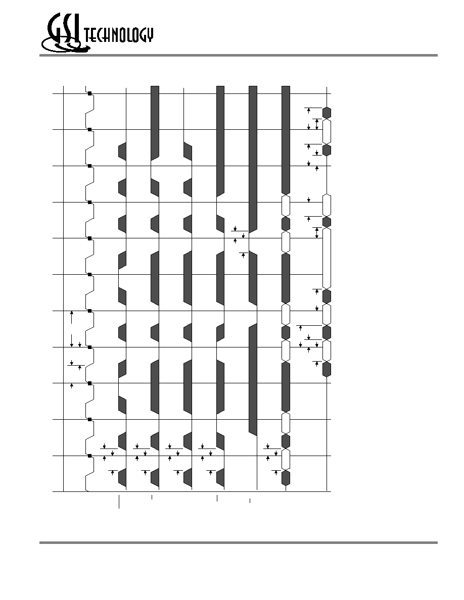
Pipeline Mode Timing (NBT)
Wri
t
e
A
R
e
a
d
B
S
u
s
pe
nd
Re
ad
C
W
rite
D
S
usp
e
nd
1
W
rite
Rea
d
E
D
e
s
e
l
ec
t
tHZ
tKQX
tKQ
tLZ
tS
tKQX
tKQ
tKQ
tH
tS
tH
tS
tH
tS
tH
tS
tH
tS
tH
tS
tH
tS
tKC
tKC
tKL
tKL
tKH
tKH
AB
C
D
D(
A
)
Q
(
B
)
Q(
C
)
D(
D
)
Q(
E)
E
CK
CKE
E
ADV
W
B
n
A0
≠A
n
DQ
Rev: 1.00a 6/2003
23/36
© 2003, Giga Semiconductor, Inc.
Specifications cited are subject to change without notice. For latest documentation see http://www.gsitechnology.com.
GS8162ZV18A(B/D)/GS8162ZV36A(B/D)/GS8162ZV72A(C)
Preliminary
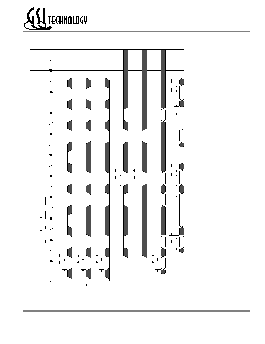
Flow Through Mode Timing (NBT)
Write A
R
e
a
d B
S
us
pen
d
Read
C
W
rite D1
Susp
en
d1
Write
Re
ad E
D
e
s
elect
tHZ
tKQX
tLZ
tHZ
tKQX
tKQ
tH
tS
tH
tS
tH
tS
tH
tS
tH
tS
tH
tS
tH
tS
tKC
tKC
tKL
tKL
tKH
tKH
AB
C
D
E
D(A)
Q(B)
Q(C)
D(D
)
Q
(
E)
CK
CKE
E
ADV
W
B
n
A0
≠A
n
DQ
Rev: 1.00a 6/2003
24/36
© 2003, Giga Semiconductor, Inc.
Specifications cited are subject to change without notice. For latest documentation see http://www.gsitechnology.com.
GS8162ZV18A(B/D)/GS8162ZV36A(B/D)/GS8162ZV72A(C)
Preliminary
JTAG Port Operation
Overview
The JTAG Port on this RAM operates in a manner that is compliant with IEEE Standard 1149.1-1990, a serial boundary scan
interface standard (commonly referred to as JTAG). The JTAG Port input interface levels scale with V
DD
. The JTAG output
drivers are powered by V
DDQ
.
Disabling the JTAG Port
It is possible to use this device without utilizing the JTAG port. The port is reset at power-up and will remain inactive unless
clocked. TCK, TDI, and TMS are designed with internal pull-up circuits.To assure normal operation of the RAM with the JTAG
Port unused, TCK, TDI, and TMS may be left floating or tied to either V
DD
or V
SS
. TDO should be left unconnected.
JTAG Port Registers
Overview
The various JTAG registers, refered to as Test Access Port orTAP Registers, are selected (one at a time) via the sequences of 1s and
0s applied to TMS as TCK is strobed. Each of the TAP Registers is a serial shift register that captures serial input data on the rising
edge of TCK and pushes serial data out on the next falling edge of TCK. When a register is selected, it is placed between the TDI
and TDO pins.
Instruction Register
The Instruction Register holds the instructions that are executed by the TAP controller when it is moved into the Run, Test/Idle, or
the various data register states. Instructions are 3 bits long. The Instruction Register can be loaded when it is placed between the
TDI and TDO pins. The Instruction Register is automatically preloaded with the IDCODE instruction at power-up or whenever the
controller is placed in Test-Logic-Reset state.
JTAG Pin Descriptions
Pin
Pin Name
I/O
Description
TCK
Test Clock
In
Clocks all TAP events. All inputs are captured on the rising edge of TCK and all outputs propagate
from the falling edge of TCK.
TMS
Test Mode Select
In
The TMS input is sampled on the rising edge of TCK. This is the command input for the TAP
controller state machine. An undriven TMS input will produce the same result as a logic one input
level.
TDI
Test Data In
In
The TDI input is sampled on the rising edge of TCK. This is the input side of the serial registers
placed between TDI and TDO. The register placed between TDI and TDO is determined by the
state of the TAP Controller state machine and the instruction that is currently loaded in the TAP
Instruction Register (refer to the TAP Controller State Diagram). An undriven TDI pin will produce
the same result as a logic one input level.
TDO
Test Data Out
Out
Output that is active depending on the state of the TAP state machine. Output changes in
response to the falling edge of TCK. This is the output side of the serial registers placed between
TDI and TDO.
Note:
This device does not have a TRST (TAP Reset) pin. TRST is optional in IEEE 1149.1. The Test-Logic-Reset state is entered while TMS is
held high for five rising edges of TCK. The TAP Controller is also reset automaticly at power-up.
Rev: 1.00a 6/2003
25/36
© 2003, Giga Semiconductor, Inc.
Specifications cited are subject to change without notice. For latest documentation see http://www.gsitechnology.com.
GS8162ZV18A(B/D)/GS8162ZV36A(B/D)/GS8162ZV72A(C)
Preliminary
Bypass Register
The Bypass Register is a single bit register that can be placed between TDI and TDO. It allows serial test data to be passed through
the RAM's JTAG Port to another device in the scan chain with as little delay as possible.
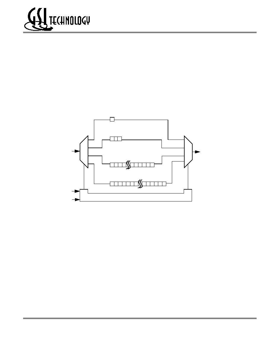
Boundary Scan Register
The Boundary Scan Register is a collection of flip flops that can be preset by the logic level found on the RAM's input or I/O pins.
The flip flops are then daisy chained together so the levels found can be shifted serially out of the JTAG Port's TDO pin. The
Boundary Scan Register also includes a number of place holder flip flops (always set to a logic 1). The relationship between the
device pins and the bits in the Boundary Scan Register is described in the Scan Order Table following. The Boundary Scan
Register, under the control of the TAP Controller, is loaded with the contents of the RAMs I/O ring when the controller is in
Capture-DR state and then is placed between the TDI and TDO pins when the controller is moved to Shift-DR state. SAMPLE-Z,
SAMPLE/PRELOAD and EXTEST instructions can be used to activate the Boundary Scan Register.
JTAG TAP Block Diagram
Identification (ID) Register
The ID Register is a 32-bit register that is loaded with a device and vendor specific 32-bit code when the controller is put in
Capture-DR state with the IDCODE command loaded in the Instruction Register. The code is loaded from a 32-bit on-chip ROM.
It describes various attributes of the RAM as indicated below. The register is then placed between the TDI and TDO pins when the
controller is moved into Shift-DR state. Bit 0 in the register is the LSB and the first to reach TDO when shifting begins.
Instruction Register
ID Code Register
Boundary Scan Register
0
1
2
0
1
2
∑
∑ ∑ ∑
31 30 29
0
1
2
∑ ∑ ∑
∑ ∑ ∑
∑ ∑ ∑
n
0
Bypass Register
TDI
TDO
TMS
TCK
Test Access Port (TAP) Controller

Rev: 1.00a 6/2003
26/36
© 2003, Giga Semiconductor, Inc.
Specifications cited are subject to change without notice. For latest documentation see http://www.gsitechnology.com.
GS8162ZV18A(B/D)/GS8162ZV36A(B/D)/GS8162ZV72A(C)
Preliminary
Tap Controller Instruction Set
Overview
There are two classes of instructions defined in the Standard 1149.1-1990; the standard (Public) instructions, and device specific
(Private) instructions. Some Public instructions are mandatory for 1149.1 compliance. Optional Public instructions must be
implemented in prescribed ways. The TAP on this device may be used to monitor all input and I/O pads, and can be used to load
address, data or control signals into the RAM or to preload the I/O buffers.
When the TAP controller is placed in Capture-IR state the two least significant bits of the instruction register are loaded with 01.
When the controller is moved to the Shift-IR state the Instruction Register is placed between TDI and TDO. In this state the desired
instruction is serially loaded through the TDI input (while the previous contents are shifted out at TDO). For all instructions, the
TAP executes newly loaded instructions only when the controller is moved to Update-IR state. The TAP instruction set for this
device is listed in the following table.
ID Register Contents
Die
Revision
Code
Not Used
I/O
Configuration
GSI Technology
JEDEC Vendor
ID Code
Presence Register
Bit # 31 30 29 28 27 26 25 24 23 22 21 20 19 18 17 16 15 14 13 12 11 10 9 8 7 6 5 4 3 2 1
0
x72
X X X X
0
0
0
0
0
0
0
0
0
0
0
0
1
0
0
1
0
0 0 1 1 0 1 1 0 0 1
1
x36
X X X X
0
0
0
0
0
0
0
0
0
0
0
0
1
0
0
0
0
0 0 1 1 0 1 1 0 0 1
1
x32
X X X X
0
0
0
0
0
0
0
0
0
0
0
0
1
1
0
0
0
0 0 1 1 0 1 1 0 0 1
1
x18
X X X X
0
0
0
0
0
0
0
0
0
0
0
0
1
0
1
0
0
0 0 1 1 0 1 1 0 0 1
1
x16
X X X X
0
0
0
0
0
0
0
0
0
0
0
0
1
1
1
0
0
0 0 1 1 0 1 1 0 0 1
1
Rev: 1.00a 6/2003
27/36
© 2003, Giga Semiconductor, Inc.
Specifications cited are subject to change without notice. For latest documentation see http://www.gsitechnology.com.
GS8162ZV18A(B/D)/GS8162ZV36A(B/D)/GS8162ZV72A(C)
Preliminary
JTAG Tap Controller State Diagram
Instruction Descriptions
BYPASS
When the BYPASS instruction is loaded in the Instruction Register the Bypass Register is placed between TDI and TDO. This occurs when
the TAP controller is moved to the Shift-DR state. This allows the board level scan path to be shortened to facilitate testing of other devices
in the scan path.
SAMPLE/PRELOAD
SAMPLE/PRELOAD is a Standard 1149.1 mandatory public instruction. When the SAMPLE / PRELOAD instruction is loaded in the Instruc-
tion Register, moving the TAP controller into the Capture-DR state loads the data in the RAMs input and I/O buffers into the Boundary Scan
Register. Boundary Scan Register locations are not associated with an input or I/O pin, and are loaded with the default state identified in the
Boundary Scan Chain table at the end of this section of the datasheet. Because the RAM clock is independent from the TAP Clock (TCK) it
is possible for the TAP to attempt to capture the I/O ring contents while the input buffers are in transition (i.e. in a metastable state). Although
allowing the TAP to sample metastable inputs will not harm the device, repeatable results cannot be expected. RAM input signals must be
stabilized for long enough to meet the TAPs input data capture set-up plus hold time (tTS plus tTH). The RAMs clock inputs need not be
paused for any other TAP operation except capturing the I/O ring contents into the Boundary Scan Register. Moving the controller to Shift-
DR state then places the boundary scan register between the TDI and TDO pins.
EXTEST
EXTEST is an IEEE 1149.1 mandatory public instruction. It is to be executed whenever the instruction register is loaded with all logic 0s. The
EXTEST command does not block or override the RAM's input pins; therefore, the RAM's internal state is still determined by its input pins.
Select DR
Capture DR
Shift DR
Exit1 DR
Pause DR
Exit2 DR
Update DR
Select IR
Capture IR
Shift IR
Exit1 IR
Pause IR
Exit2 IR
Update IR
Test Logic Reset
Run Test Idle
0
0
1
0
1
1
0
0
1
1
1
0
0
1
1
0
0
0
0
1
1
0
0
1
1
0
0
0
1
1
1
1

Rev: 1.00a 6/2003
28/36
© 2003, Giga Semiconductor, Inc.
Specifications cited are subject to change without notice. For latest documentation see http://www.gsitechnology.com.
GS8162ZV18A(B/D)/GS8162ZV36A(B/D)/GS8162ZV72A(C)
Preliminary
Typically, the Boundary Scan Register is loaded with the desired pattern of data with the SAMPLE/PRELOAD command. Then the EXTEST
command is used to output the Boundary Scan Register's contents, in parallel, on the RAM's data output drivers on the falling edge of TCK when
the controller is in the Update-IR state.
Alternately, the Boundary Scan Register may be loaded in parallel using the EXTEST command. When the EXTEST instruction is selected, the
sate of all the RAM's input and I/O pins, as well as the default values at Scan Register locations not associated with a pin, are transferred in
parallel into the Boundary Scan Register on the rising edge of TCK in the Capture-DR state, the RAM's output pins drive out the value of the
Boundary Scan Register location with which each output pin is associated.
IDCODE
The IDCODE instruction causes the ID ROM to be loaded into the ID register when the controller is in Capture-DR mode and places the ID
register between the TDI and TDO pins in Shift-DR mode. The IDCODE instruction is the default instruction loaded in at power up and any
time the controller is placed in the Test-Logic-Reset state.
SAMPLE-Z
If the SAMPLE-Z instruction is loaded in the instruction register, all RAM outputs are forced to an inactive drive state (high-Z) and the Bound-
ary Scan Register is connected between TDI and TDO when the TAP controller is moved to the Shift-DR state.
RFU
These instructions are Reserved for Future Use. In this device they replicate the BYPASS instruction.
JTAG TAP Instruction Set Summary
Instruction
Code
Description
Notes
EXTEST
000
Places the Boundary Scan Register between TDI and TDO.
1
IDCODE
001
Preloads ID Register and places it between TDI and TDO.
1, 2
SAMPLE-Z
010
Captures I/O ring contents. Places the Boundary Scan Register between TDI and
TDO.
Forces all RAM output drivers to High-Z.
1
RFU
011
Do not use this instruction; Reserved for Future Use.
Replicates BYPASS instruction. Places Bypass Register between TDI and TDO.
1
SAMPLE/
PRELOAD
100
Captures I/O ring contents. Places the Boundary Scan Register between TDI and
TDO.
1
GSI
101
GSI private instruction.
1
RFU
110
Do not use this instruction; Reserved for Future Use.
Replicates BYPASS instruction. Places Bypass Register between TDI and TDO.
1
BYPASS
111
Places Bypass Register between TDI and TDO.
1
Notes:
1. Instruction codes expressed in binary, MSB on left, LSB on right.
2. Default instruction automatically loaded at power-up and in test-logic-reset state.
Rev: 1.00a 6/2003
29/36
© 2003, Giga Semiconductor, Inc.
Specifications cited are subject to change without notice. For latest documentation see http://www.gsitechnology.com.
GS8162ZV18A(B/D)/GS8162ZV36A(B/D)/GS8162ZV72A(C)
Preliminary
JTAG Port Recommended Operating Conditions and DC Characteristics
Parameter
Symbol
Min.
Max.
Unit Notes
1.8 V Test Port Input High Voltage
V
IHJ
0.6 * V
DD
V
DD
+0.3
V
1
1.8 V Test Port Input Low Voltage
V
ILJ
≠0.3
0.3 * V
DD
V
1
TMS, TCK and TDI Input Leakage Current
I
INHJ
≠300
1
uA
2
TMS, TCK and TDI Input Leakage Current
I
INLJ
≠1
100
uA
3
TDO Output Leakage Current
I
OLJ
≠1
1
uA
4
Test Port Output High Voltage
V
OHJ
1.7
--
V
5, 6
Test Port Output Low Voltage
V
OLJ
--
0.4
V
5, 7
Test Port Output CMOS High
V
OHJC
V
DDQ
≠ 100 mV
--
V
5, 8
Test Port Output CMOS Low
V
OLJC
--
100 mV
V
5, 9
Notes:
1. Input Under/overshoot voltage must be ≠2 V > Vi < V
DDn
+2 V not to exceed 3.6 V maximum, with a pulse width not to exceed 20% tTKC.
2. V
ILJ
V
IN
V
DDn
3. 0 V
V
IN
V
ILJn
4. Output Disable, V
OUT
= 0 to V
DDn
5. The TDO output driver is served by the V
DDQ
supply.
6. I
OHJ
= ≠4 mA
7. I
OLJ
= + 4 mA
8. I
OHJC
= ≠100 uA
9. I
OHJC
= +100 uA
Notes:
1. Include scope and jig capacitance.
2. Test conditions as as shown unless otherwise noted.
JTAG Port AC Test Conditions
Parameter
Conditions
Input high level
V
DD
≠ 0.2 V
Input low level
0.2 V
Input slew rate
1 V/ns
Input reference level
V
DDQ
/2
Output reference level
V
DDQ
/2
DQ
V
DDQ
/2
50
30pF
*
JTAG Port AC Test Load
* Distributed Test Jig Capacitance
Rev: 1.00a 6/2003
30/36
© 2003, Giga Semiconductor, Inc.
Specifications cited are subject to change without notice. For latest documentation see http://www.gsitechnology.com.
GS8162ZV18A(B/D)/GS8162ZV36A(B/D)/GS8162ZV72A(C)
Preliminary
JTAG Port Timing Diagram
JTAG Port AC Electrical Characteristics
Boundary Scan (BSDL Files)
For information regarding the Boundary Scan Chain, or to obtain BSDL files for this part, please contact our Applications
Engineering Department at: apps@gsitechnology.com.
Parameter
Symbol
Min
Max
Unit
TCK Cycle Time
tTKC
50
--
ns
TCK Low to TDO Valid
tTKQ
--
20
ns
TCK High Pulse Width
tTKH
20
--
ns
TCK Low Pulse Width
tTKL
20
--
ns
TDI & TMS Set Up Time
tTS
10
--
ns
TDI & TMS Hold Time
tTH
10
--
ns
tTKQ
tTS
tTH
tTKH
tTKL
TCK
TMS
TDI
TDO
tTKC
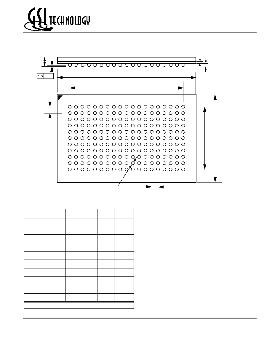
Rev: 1.00a 6/2003
31/36
© 2003, Giga Semiconductor, Inc.
Specifications cited are subject to change without notice. For latest documentation see http://www.gsitechnology.com.
GS8162ZV18A(B/D)/GS8162ZV36A(B/D)/GS8162ZV72A(C)
Preliminary
209 BGA Package Drawing (Package C)
14 mm x 22 mm Body, 1.0 mm Bump Pitch, 11 x 19 Bump Array
Symbol
Min
Typ
Max
Units
A
--
--
1.70
mm
A1
0.40
0.50
0.60
mm
b
0.50
0.60
0.70
mm
c
0.31
0.36
0.38
mm
D
21.9
22.0
22.1
mm
D1
--
18.0 (BSC)
--
mm
E
13.9
14.0
14.1
mm
E1
--
10.0 (BSC)
--
mm
e
--
1.00 (BSC)
--
mm
aaa
--
0.15
--
mm
Rev 1.0
A
A1
C
b
e
e
E
E1
D1
D
aaa
Bottom View
Side View
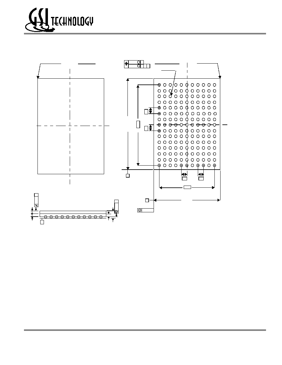
Rev: 1.00a 6/2003
32/36
© 2003, Giga Semiconductor, Inc.
Specifications cited are subject to change without notice. For latest documentation see http://www.gsitechnology.com.
GS8162ZV18A(B/D)/GS8162ZV36A(B/D)/GS8162ZV72A(C)
Preliminary
Package Dimensions--165-Bump FPBGA (Package D)
A
B
C
D
E
F
G
H
I
J
K
L
M
N
P
R
A
B
C
D
E
F
G
H
J
K
L
M
N
P
R
1 2 3 4 5 6 7 8 9 10 11
11 10 9 8 7 6 5 4 3 2 1
A1 CORNER
TOP VIEW
A1 CORNER
BOTTOM VIEW
1.0
1.0
10.0
1.
0
1.
0
14
.0
13±0.07
15±0.
07
A
B
0.20(4x)
ÿ0.10
ÿ0.25
C
C A B
M
M
ÿ0.40~0.50 (165x)
C
SEATING PLANE
0.
15
C
0.
25
~0.
4
0
1.2
0
MA
X.
0.
45±0.
05
0.
25
C
(0
.2
6)
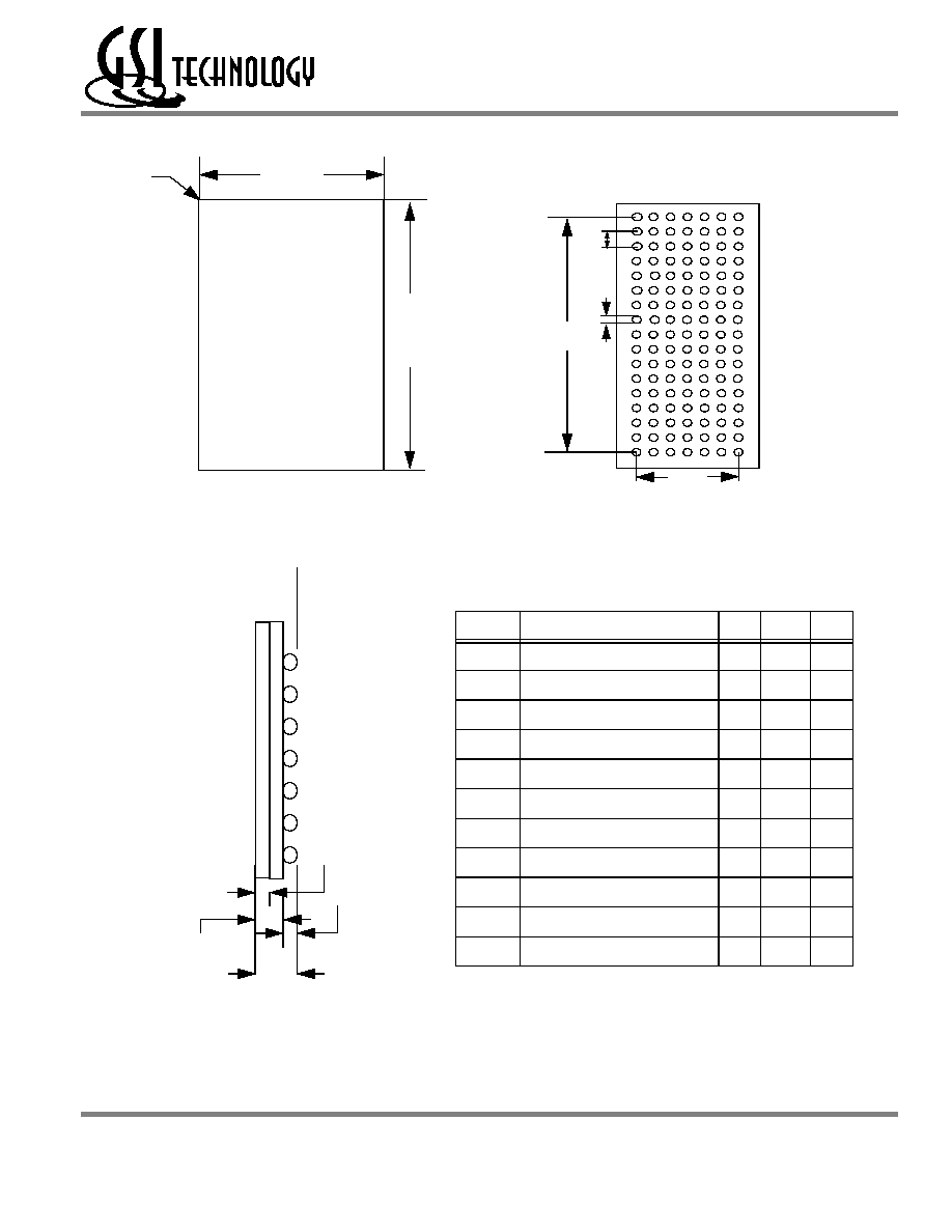
Rev: 1.00a 6/2003
33/36
© 2003, Giga Semiconductor, Inc.
Specifications cited are subject to change without notice. For latest documentation see http://www.gsitechnology.com.
GS8162ZV18A(B/D)/GS8162ZV36A(B/D)/GS8162ZV72A(C)
Preliminary
Package Dimensions--119-Pin PBGA (Package B)
BPR 1999.05.18
A
B
Pin 1
Corner
K
E
F
CT
A
B
C
D
E
F
G
H
J
K
L
M
N
P
R
T
U
G
S
D
1
2
3
4
5
6
7
Package Dimensions--119-Pin PBGA
Unit: mm
Symbol
Description
Min. Nom. Max
A
Width
13.9
14.0
14.1
B
Length
21.9
22.0
22.1
C
Package Height (including ball)
1.73
1.86
1.99
D
Ball Size
0.60
0.75
0.90
E
Ball Height
0.50
0.60
0.70
F
Package Height (excluding balls) 1.16
1.26
1.36
G
Width between Balls
1.27
K
Package Height above board
0.65
0.70
0.75
R
Width of package between balls
7.62
S
Length of package between balls
20.32
T
Variance of Ball Height
0.15
Bottom View
R
Top View
Side View
A
B
C
D
E
F
G
H
J
K
L
M
N
P
R
T
U
Rev: 1.00a 6/2003
34/36
© 2003, Giga Semiconductor, Inc.
Specifications cited are subject to change without notice. For latest documentation see http://www.gsitechnology.com.
GS8162ZV18A(B/D)/GS8162ZV36A(B/D)/GS8162ZV72A(C)
Preliminary
Ordering Information--GSI NBT Synchronous SRAM
Org
Part Number
1
Type
Package
Speed
2
(MHz/ns)
T
A
3
Status
1M x 18
GS8162ZV18AB-350
NBT Pipeline/Flow Through
119 BGA
350/4.5
C
1M x 18
GS8162ZV18AB-333
NBT Pipeline/Flow Through
119 BGA
333/4.7
C
1M x 18
GS8162ZV18AB-300
NBT Pipeline/Flow Through
119 BGA
300/5
C
1M x 18
GS8162ZV18AB-250
NBT Pipeline/Flow Through
119 BGA
250/5.5
C
1M x 18
GS8162ZV18AB-200
NBT Pipeline/Flow Through
119 BGA
200/6.5
C
1M x 18
GS8162ZV18AB-150
NBT Pipeline/Flow Through
119 BGA
150/7.5
C
512K x 36
GS8162ZV36AB-350
NBT Pipeline/Flow Through
119 BGA
350/4.5
C
512K x 36
GS8162ZV36AB-333
NBT Pipeline/Flow Through
119 BGA
333/4.7
C
512K x 36
GS8162ZV36AB-300
NBT Pipeline/Flow Through
119 BGA
300/5
C
512K x 36
GS8162ZV36AB-250
NBT Pipeline/Flow Through
119 BGA
250/5.5
C
512K x 36
GS8162ZV36AB-200
NBT Pipeline/Flow Through
119 BGA
200/6.5
C
512K x 36
GS8162ZV36AB-150
NBT Pipeline/Flow Through
119 BGA
150/7.5
C
1M x 18
GS8162ZV18AD-350
NBT Pipeline/Flow Through
165 BGA
350/4.5
C
1M x 18
GS8162ZV18AD-333
NBT Pipeline/Flow Through
165 BGA
333/4.7
C
1M x 18
GS8162ZV18AD-300
NBT Pipeline/Flow Through
165 BGA
300/5
C
1M x 18
GS8162ZV18AD-250
NBT Pipeline/Flow Through
165 BGA
250/5.5
C
1M x 18
GS8162ZV18AD-200
NBT Pipeline/Flow Through
165 BGA
200/6.5
C
1M x 18
GS8162ZV18AD-150
NBT Pipeline/Flow Through
165 BGA
150/7.5
C
512K x 36
GS8162ZV36AD-350
NBT Pipeline/Flow Through
165 BGA
350/4.5
C
512K x 36
GS8162ZV36AD-333
NBT Pipeline/Flow Through
165 BGA
333/4.7
C
512K x 36
GS8162ZV36AD-300
NBT Pipeline/Flow Through
165 BGA
300/5
C
512K x 36
GS8162ZV36AD-250
NBT Pipeline/Flow Through
165 BGA
250/5.5
C
512K x 36
GS8162ZV36AD-200
NBT Pipeline/Flow Through
165 BGA
200/6.5
C
512K x 36
GS8162ZV36AD-150
NBT Pipeline/Flow Through
165 BGA
150/7.5
C
256K x 72
GS8162ZV72AC-300
NBT Pipeline/Flow Through
209 BGA
300/5
C
256K x 72
GS8162ZV72AC-250
NBT Pipeline/Flow Through
209 BGA
250/5.5
C
256K x 72
GS8162ZV72AC-200
NBT Pipeline/Flow Through
209 BGA
200/6.5
C
256K x 72
GS8162ZV72AC-150
NBT Pipeline/Flow Through
209 BGA
150/7.5
C
1M x 18
GS8162ZV18AB-350I
NBT Pipeline/Flow Through
119 BGA
350/4.5
I
Notes:
1. Customers requiring delivery in Tape and Reel should add the character "T" to the end of the part number. Example: GS8162ZV36AB-
200IT.
2. The speed column indicates the cycle frequency (MHz) of the device in Pipeline mode and the latency (ns) in Flow Through mode. Each
device is Pipeline/Flow Through mode-selectable by the user.
3. T
A
= C = Commercial Temperature Range. T
A
= I = Industrial Temperature Range.
4. GSI offers other versions this type of device in many different configurations and with a variety of different features, only some of which
are covered in this data sheet. See the GSI Technology web site (www.gsitechnology.com) for a complete listing of current offerings
Rev: 1.00a 6/2003
35/36
© 2003, Giga Semiconductor, Inc.
Specifications cited are subject to change without notice. For latest documentation see http://www.gsitechnology.com.
GS8162ZV18A(B/D)/GS8162ZV36A(B/D)/GS8162ZV72A(C)
Preliminary
1M x 18
GS8162ZV18AB-333I
NBT Pipeline/Flow Through
119 BGA
333/4.7
I
1M x 18
GS8162ZV18AB-300I
NBT Pipeline/Flow Through
119 BGA
300/5
I
1M x 18
GS8162ZV18AB-250I
NBT Pipeline/Flow Through
119 BGA
250/5.5
I
1M x 18
GS8162ZV18AB-200I
NBT Pipeline/Flow Through
119 BGA
200/6.5
I
1M x 18
GS8162ZV18AB-150I
NBT Pipeline/Flow Through
119 BGA
150/7.5
I
512K x 36
GS8162ZV36AB-350I
NBT Pipeline/Flow Through
119 BGA
350/4.5
I
512K x 36
GS8162ZV36AB-333I
NBT Pipeline/Flow Through
119 BGA
333/4.7
I
512K x 36
GS8162ZV36AB-300I
NBT Pipeline/Flow Through
119 BGA
300/5
I
512K x 36
GS8162ZV36AB-250I
NBT Pipeline/Flow Through
119 BGA
250/5.5
I
512K x 36
GS8162ZV36AB-200I
NBT Pipeline/Flow Through
119 BGA
200/6.5
I
512K x 36
GS8162ZV36AB-150I
NBT Pipeline/Flow Through
119 BGA
150/7.5
I
1M x 18
GS8162ZV18AD-350I
NBT Pipeline/Flow Through
165 BGA
350/4.5
I
1M x 18
GS8162ZV18AD-333I
NBT Pipeline/Flow Through
165 BGA
333/4.7
I
1M x 18
GS8162ZV18AD-300I
NBT Pipeline/Flow Through
165 BGA
300/5
I
1M x 18
GS8162ZV18AD-250I
NBT Pipeline/Flow Through
165 BGA
250/5.5
I
1M x 18
GS8162ZV18AD-200I
NBT Pipeline/Flow Through
165 BGA
200/6.5
I
1M x 18
GS8162ZV18AD-150I
NBT Pipeline/Flow Through
165 BGA
150/7.5
I
512K x 36
GS8162ZV36AD-350I
NBT Pipeline/Flow Through
165 BGA
350/4.5
I
512K x 36
GS8162ZV36AD-333I
NBT Pipeline/Flow Through
165 BGA
333/4.7
I
512K x 36
GS8162ZV36AD-300I
NBT Pipeline/Flow Through
165 BGA
300/5
I
512K x 36
GS8162ZV36AD-250I
NBT Pipeline/Flow Through
165 BGA
250/5.5
I
512K x 36
GS8162ZV36AD-200I
NBT Pipeline/Flow Through
165 BGA
200/6.5
I
512K x 36
GS8162ZV36AD-150I
NBT Pipeline/Flow Through
165 BGA
150/7.5
I
256K x 72
GS8162ZV72AC-300I
NBT Pipeline/Flow Through
209 BGA
300/5
I
256K x 72
GS8162ZV72AC-250I
NBT Pipeline/Flow Through
209 BGA
250/5.5
I
256K x 72
GS8162ZV72AC-200I
NBT Pipeline/Flow Through
209 BGA
200/6.5
I
256K x 72
GS8162ZV72AC-150I
NBT Pipeline/Flow Through
209 BGA
150/7.5
I
Org
Part Number
1
Type
Package
Speed
2
(MHz/ns)
T
A
3
Status
Notes:
1. Customers requiring delivery in Tape and Reel should add the character "T" to the end of the part number. Example: GS8162ZV36AB-
200IT.
2. The speed column indicates the cycle frequency (MHz) of the device in Pipeline mode and the latency (ns) in Flow Through mode. Each
device is Pipeline/Flow Through mode-selectable by the user.
3. T
A
= C = Commercial Temperature Range. T
A
= I = Industrial Temperature Range.
4. GSI offers other versions this type of device in many different configurations and with a variety of different features, only some of which
are covered in this data sheet. See the GSI Technology web site (www.gsitechnology.com) for a complete listing of current offerings

Rev: 1.00a 6/2003
36/36
© 2003, Giga Semiconductor, Inc.
Specifications cited are subject to change without notice. For latest documentation see http://www.gsitechnology.com.
GS8162ZV18A(B/D)/GS8162ZV36A(B/D)/GS8162ZV72A(C)
Preliminary
18Mb Sync SRAM Datasheet Revision History
DS/DateRev. Code: Old;
New
Types of Changes
Format or Content
Page;Revisions;Reason
GS8162ZVxxA_r1
∑ Creation of new datasheet