8170xxxx_r2.01_draft_20030328.fm
Rev: 2.01 5/2003
1/29
© 2002, GSI Technology, Inc.
Specifications cited are design targets and are subject to change without notice. For latest documentation contact your GSI representative.
Preliminary
GS8170DD36C-333/300/250/200
18Mb
1x2Lp CMOS I/O
Double Data Rate SigmaRAMTM
200 MHz333 MHz
1.8 V V
DD
1.8 V I/O
209-Bump BGA
Commercial Temp
Industrial Temp
Features
· Double Data Rate Read and Write mode
· Late Write; Pipelined read operation
· JEDEC-standard SigmaRAM
TM
pinout and package
· 1.8 V +150/100 mV core power supply
· 1.8 V CMOS Interface
· ZQ controlled user-selectable output drive strength
· Dual Cycle Deselect
· Burst Read and Write option
· Fully coherent read and write pipelines
· Echo Clock outputs track data output drivers
· 2 user-programmable chip enable inputs
· IEEE 1149.1 JTAG-compliant Serial Boundary Scan
· 209-bump, 14 mm x 22 mm, 1 mm bump pitch BGA package
· Pin-compatible with future 36Mb, 72Mb, and 144Mb
devices
SigmaRAM Family Overview
GS8170DD36 SigmaRAMs are built in compliance with the
SigmaRAM pinout standard for synchronous SRAMs. They
are 18,874,368-bit (18Mb) SRAMs. This family of wide, very
low voltage CMOS I/O SRAMs is designed to operate at the
speeds needed to implement economical high performance
networking systems.
RAMs are offered in a number of configurations including
Late Write, Double Late Write, and Double Data Rate (DDR).
The logical differences between the protocols employed by
these RAMs mainly involve various approaches to write
cueing and data transfer rates. The
RAM
TM
family standard
allows a user to implement the interface protocol best suited to
the task at hand.
Functional Description
Because SigmaRAMs are synchronous devices, address data
inputs and read/write control inputs are captured on the rising
edge of the input clock. Write cycles are internally self-timed
and initiated by the rising edge of the clock input. This feature
eliminates complex off-chip write pulse generation required by
asynchronous SRAMs and simplifies input signal timing. In
DDR mode the device captures Data In on both rising and
falling edges of clock and drives data on both clock edges as
well.
Because the DDR
RAM always transfers data in two halves,
A0 is internally set to 0 for the first half of each read or write
transfer, and automatically incremented to 1 for the falling
edge transfer. The address field of a DDR
RAM is always
one address pin less than the advertised index depth (e.g., the
512k x 36 has a 512k addressable index).
RAMs support pipelined reads utilizing a rising-edge-
triggered output register. DDR
RAMs incorporate rising-
and falling-edge-triggered output registers. They also utilize a
Dual Cycle Deselect (DCD) output deselect protocol.
RAMs are implemented with high performance CMOS
technology and are packaged in a 209-bump BGA.
Key Fast Bin Specs
Symbol
- 333
Cycle Time
tKHKH
3.0 ns
Access Time
tKHQV
1.8 ns
209-Bump, 14 mm x 22 mm BGA
1 mm Bump Pitch, 11 x 19 Bump Array
Bottom View
Rev: 2.01 5/2003
2/29
© 2002, GSI Technology, Inc.
Specifications cited are design targets and are subject to change without notice. For latest documentation contact your GSI representative.
Preliminary
GS8170DD36C-333/300/250/200
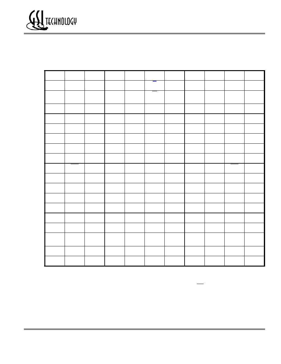
SigmaRAM Pinouts
512k x 36 Common I/O--Top View
1
2
3
4
5
6
7
8
9
10
11
A NC
NC
A
E2
A
ADV
A
E3
A
DQb
DQb
B NC
NC
MCL
NC
A
W
A
MCL
NC
DQb
DQb
C NC
NC
NC
MCL
NC
(144M)
E1
NC
NC
MCL
DQb
DQb
D NC
NC
V
SS
NC
NC
MCL
NC
NC
V
SS
DQb
DQb
E NC
DQc
V
DDQ
V
DDQ
V
DD
V
DD
V
DD
V
DDQ
V
DDQ
NC
DQb
F DQc
DQc
V
SS
V
SS
V
SS
ZQ
V
SS
V
SS
V
SS
NC
NC
G DQc
DQc
V
DDQ
V
DDQ
V
DD
EP2
V
DD
V
DDQ
V
DDQ
NC
NC
H DQc
DQc
V
SS
V
SS
V
SS
EP3
V
SS
V
SS
V
SS
NC
NC
J DQc
DQc
V
DDQ
V
DDQ
V
DD
MCH
V
DD
V
DDQ
V
DDQ
NC
NC
K
CQ2
CQ2
CK
NC
V
SS
MCL
V
SS
NC
NC
CQ1
CQ1
L NC
NC
V
DDQ
V
DDQ
V
DD
MCL
V
DD
V
DDQ
V
DDQ
DQa
DQa
M NC
NC
V
SS
V
SS
V
SS
MCH
V
SS
V
SS
V
SS
DQa
DQa
N NC
NC
V
DDQ
V
DDQ
V
DD
MCH
V
DD
V
DDQ
V
DDQ
DQa
DQa
P NC
NC
V
SS
V
SS
V
SS
MCL
V
SS
V
SS
V
SS
DQa
DQa
R DQd
NC
V
DDQ
V
DDQ
V
DD
V
DD
V
DD
V
DDQ
V
DDQ
DQa
NC
T DQd
DQd
V
SS
NC
NC
MCL
NC
NC
V
SS
NC
NC
U DQd
DQd
NC
A
NC
(72M)
A
NC
(36M)
A
NC
NC
NC
V
DQd
DQd
A
A
A
A1
A
A
A
NC
NC
W
DQd
DQd
TMS
TDI
A
MCL
A
TDO
TCK
NC
NC
· 2002.06
11 x 19 Bump BGA--14 x 22 mm
2
Body--1 mm Bump Pitch
·
Note:
Users of CMOS I/O SigmaRAMs may wish to connect "NC, V
REF
" and the "NC, CK" pins to V
REF
(i.e., V
DDQ
/2) to
allow alternate use of future HSTL I/O SigmaRAMs.
Rev: 2.01 5/2003
3/29
© 2002, GSI Technology, Inc.
Specifications cited are design targets and are subject to change without notice. For latest documentation contact your GSI representative.
Preliminary
GS8170DD36C-333/300/250/200
Operation Control
All address, data and control inputs (with the exception of EP2, EP3, ZQ, and the mode pins, L6, M6, and J6) are synchronized to
rising clock edges. Data in is captured on both rising and falling edges of CK. Read and write operations must be initiated with the
Advance/Load pin (ADV) held low, in order to load the new address. Device activation is accomplished by asserting all three of the
Chip Enable inputs (E1, E2, and E3). Deassertion of any one of the Enable inputs will deactivate the device. It should be noted
that ONLY deactivation of the RAM via E2 and/or E3 deactivates the Echo Clocks, CQ1CQ2.
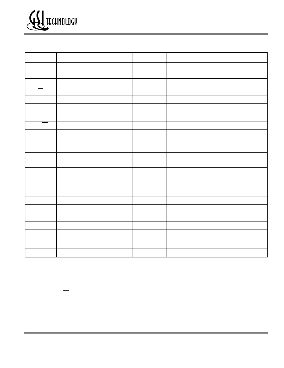
Pin Description Table
Symbol
Description
Type
Comments
A
Address
Input
--
ADV
Advance
Input
Active High
W
Write Enable
Input
Active Low
E1
Chip Enable
Input
Active Low
E2 & E3
Chip Enable
Input
Programmable Active High or Low
EP2 & EP3
Chip Enable Program Pin
Mode Input
To be tied directly to V
DD
, V
DDQ
or V
SS
CK
Clock
Input
Active High
CQ, CQ
Echo Clock
Output
Three State - Deselect via E2 or E3 False
DQ
Data I/O
Input/Output
Three State
MCH
Must Connect High
Input
Active High
To be tied directly to V
DD
or V
DDQ
MCL
Must Connect Low
Input
Active Low
To be tied directly to V
SS
ZQ
Output Impedance Control
Mode Input
Low = Low Impedance [High Drive]
High = High Impedance [Low Drive]
To be tied directly to V
DDQ
or V
SS
TCK
Test Clock
Input
Active High
TDI
Test Data In
Input
--
TDO
Test Data Out
Output
--
TMS
Test Mode Select
Input
--
NC
No Connect
--
Not connected to die or any other pin
V
DD
Core Power Supply
Input
1.8 V Nominal
V
DDQ
Output Driver Power Supply
Input
1.8 V Nominal
V
SS
Ground
Input
--
Rev: 2.01 5/2003
4/29
© 2002, GSI Technology, Inc.
Specifications cited are design targets and are subject to change without notice. For latest documentation contact your GSI representative.
Preliminary
GS8170DD36C-333/300/250/200
Read Operations
Double Data Rate Read
In applications where a data rate markedly faster than the RAM's latency is desired, the Double Data Rate protocol doubles the
data transfer rate (read or write bandwidth) achieved in Pipeline mode while keeping the RAM's clock frequency constant. In
Double Data Rate mode, the RAM multiplexes the results of a read out of the RAM on half the usual number of data pins. The
output register/mux behaves just as if it were in Pipeline mode for the first transfer, but then makes a second transfer in response to
the next falling edge of clock as well. SigmaRAM DDR RAMs burst in linear order only.
Write Operations
Write operation occurs when the following conditions are satisfied at the rising edge of clock: All three chip enables (E1, E2, and
E3) are active, the write enable input signal (W) is asserted low, and ADV is asserted low.
Double Data Rate Write
A Double Data Rate Write is a specialized form of Late Write. In Double Data Rate mode, the RAM will capture Data In on both
rising and falling edges of the RAM clock, CK, beginning with the rising edge of clock that follows the capture of the write address
and command.
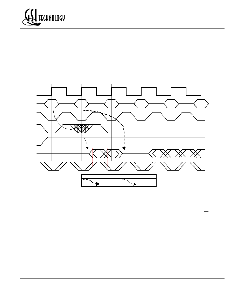
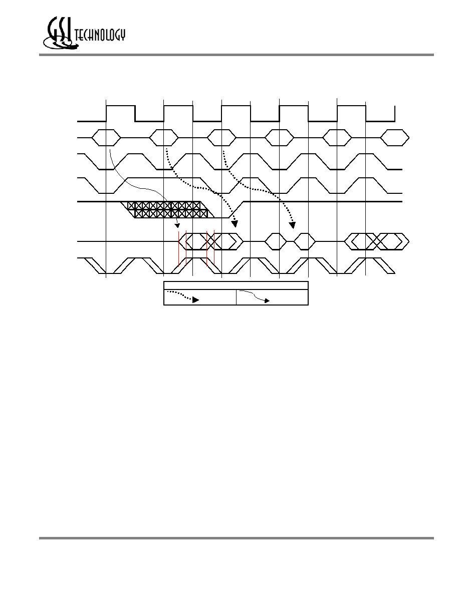
Double Data Rate Pipelined Read
QA0
QA1
QC0
QC1
QD0
QD1
CK
Read
Deselect
A
XX
F
Read
Read
Read
ADV
D
E
C
/E
1
/W
DQ
Address
CQ
Key
Hi-Z
Access
Rev: 2.01 5/2003
5/29
© 2002, GSI Technology, Inc.
Specifications cited are design targets and are subject to change without notice. For latest documentation contact your GSI representative.
Preliminary
GS8170DD36C-333/300/250/200
Special Functions
Burst Cycles
SRAMs provide an on-chip burst address generator that can be utilized, if desired, to simplify burst read or write implementations.
The ADV control pin, when driven high, commands the SRAM to advance the internal address counter and use the counter
generated address to read or write the SRAM. The starting address for the first cycle in a burst cycle series is loaded into the SRAM
by driving the ADV pin low, into Load mode.
SigmaRAM Double Data Rate Read and Write
QA0
QA1
DC0
DC1
QD0
QD1
ADV
Read
CQ
E
Deselect
C
D
Write
Read
Read
CK
Address
A
Key
Hi-Z
Access
/E
1
/W
DQ
F
B