8182Sxx_r1_01.fm
Rev: 1.01 6/2003
1/30
© 2003, Giga Semiconductor, Inc.
Specifications cited are design targets and are subject to change without notice. For latest documentation contact your GSI representative.
Preliminary
GS8182S18/36D-333/300/250/200/167
18Mb
2x1B2
DDR SigmaSIO-II SRAM
167 MHz333 MHz
1.8 V V
DD
1.8 V and 1.5 V I/O
165-Bump BGA
Commercial Temp
Industrial Temp
Features
· Simultaneous Read and Write SigmaQuadTM Interface
· JEDEC-standard pinout and package
· Dual Double Data Rate interface
· Byte Write controls sampled at data-in time
· DLL circuitry for wide output data valid window and future frequency
scaling
· Burst of 2 Read and Write
· 1.8 V +150/100 mV core power supply
· 1.5 V or 1.8 V HSTL Interface
· Pipelined read operation
· Fully coherent read and write pipelines
· ZQ mode pin for programmable output drive strength
· IEEE 1149.1 JTAG-compliant Boundary Scan
· 165-bump, 13 mm x 15 mm, 1 mm bump pitch BGA package
· Pin-compatible with future 36Mb, 72Mb, and 144Mb devices
SigmaRAMTM Family Overview
GS8182S18/36 are built in compliance with the SigmaSIO-II SRAM
pinout standard for Separate I/O synchronous SRAMs. They are
18,874,368-bit (18Mb) SRAMs. These are the first in a family of wide,
very low voltage HSTL I/O SRAMs designed to operate at the speeds
needed to implement economical high performance networking
systems.
Clocking and Addressing Schemes
A
2x1B2
SigmaSIO-II SRAM is a synchronous device. It employs a
single input register clock input, K. The device also allows the user to
manipulate the output register clock input quasi independently with
the C clock input. If the C clock is tied high, the K clock is routed
internally to fire the output registers instead. Each
2x1B2
SigmaSIO-II SRAM also supplies an Echo Clock output, CQ, which is
synchronized with read data output. When used in a source
synchronous clocking scheme, the Echo Clock output can be used to
fire input registers at the data's destination.
Because Separate I/O
2x1B2
RAMs always transfer data in two
packets, A0 is internally set to 0 for the first read or write transfer, and
automatically incremented by 1 for the next transfer. Because the LSB
is tied off internally, the address field of a
2x1B2
RAM is always one
address pin less than the advertised index depth (e.g., the 1M x 18
has a 512K addressable index).
Alternating Read-Write Operations
SigmaSIO-II SRAMs follow a few simple rules of operation.
- Read or Write commands issued on one port are never allowed to
interrupt an operation in progress on the other port.
- Read or Write data transfers in progress may not be interrupted and
re-started.
- R and W high always deselects the RAM.
- All address, data, and control inputs are sampled on clock edges.
In order to enforce these rules, each RAM combines present state
information with command inputs. See the Truth Table for details.
- 333
-300
-250
-200
-167
tKHKH
3.0 ns
3.3 ns
4.0 ns
5.0 ns
6.0 ns
tKHQV
0.45 ns
0.45 ns
.045 ns
0.45 ns
0.5 ns
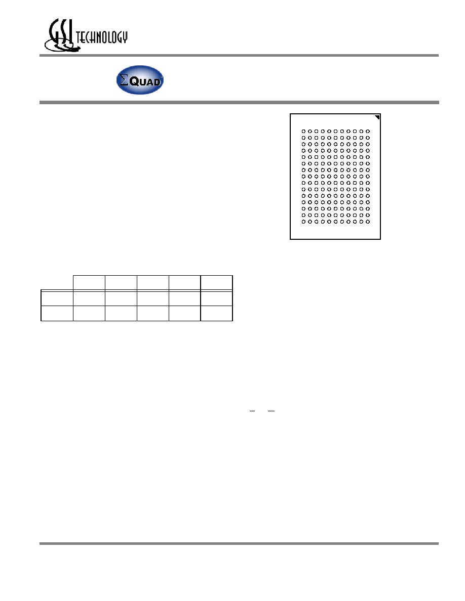
165-Bump, 13 mm x 15 mm BGA
1 mm Bump Pitch, 11 x 15 Bump Array
Bottom View
JEDEC Std. MO-216, Variation CAB-1
Rev: 1.01 6/2003
2/30
© 2003, Giga Semiconductor, Inc.
Specifications cited are design targets and are subject to change without notice. For latest documentation contact your GSI representative.
Preliminary
GS8182S18/36D-333/300/250/200/167
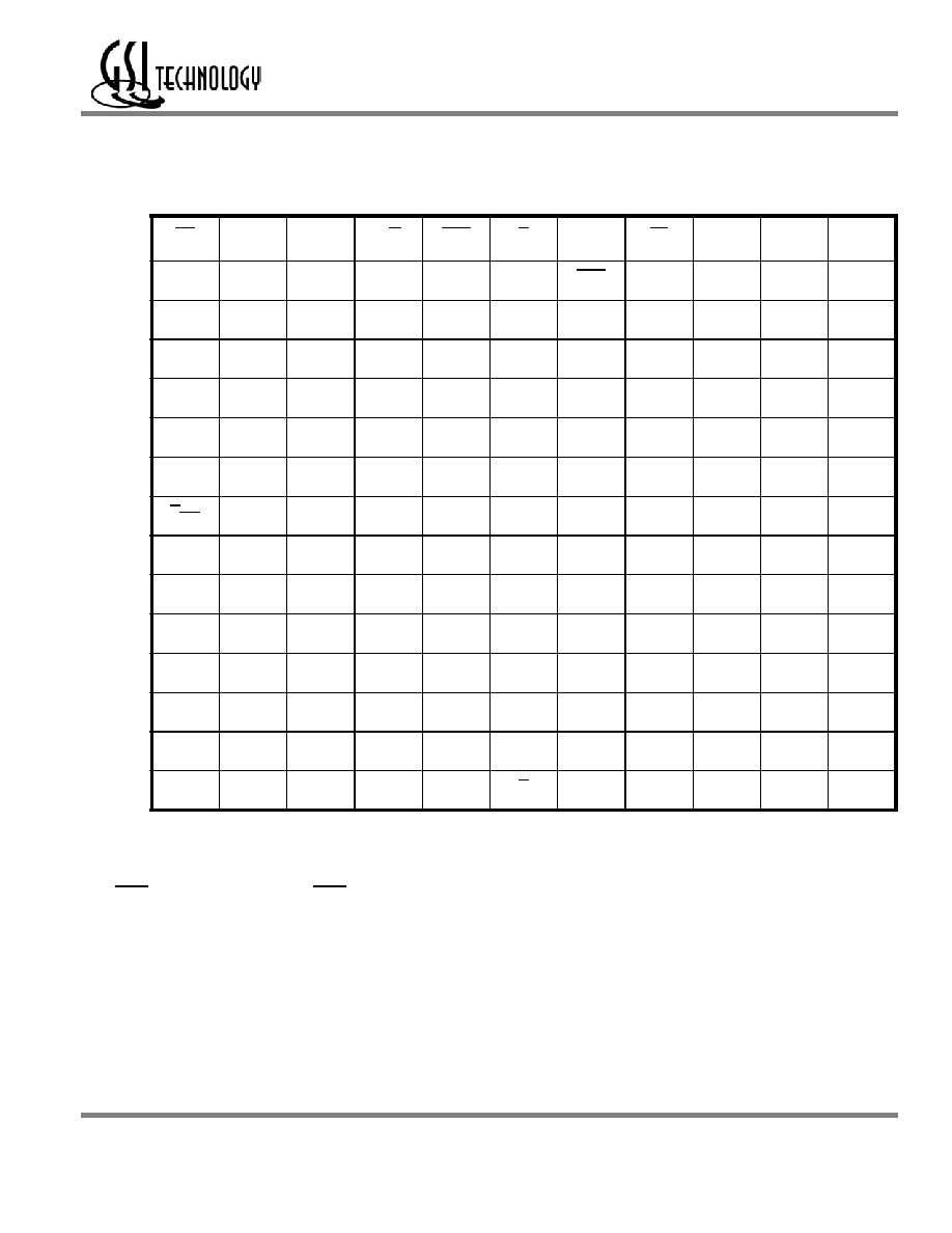
1M x 18 SigmaQuad SRAM -- Top View
1
2
3
4
5
6
7
8
9
10
11
A CQ
V
SS
/SA
(144Mb)
NC/SA
(36Mb)
R/W
BW1
K
NC
LD
SA
V
SS
/SA
(72Mb)
CQ
B NC
Q9
D9
SA
NC
K
BW0
SA
NC
NC
Q8
C NC
NC
D10
V
SS
SA
SA
SA
V
SS
NC
Q7
D8
D NC
D11
Q10
V
SS
V
SS
V
SS
V
SS
V
SS
NC
NC
D7
E NC
NC
Q11
V
DDQ
V
SS
V
SS
V
SS
V
DDQ
NC
D6
Q6
F
NC
Q12
D12
V
DDQ
V
DD
V
SS
V
DD
V
DDQ
NC
NC
Q5
G NC
D13
Q13
V
DDQ
V
DD
V
SS
V
DD
V
DDQ
NC
NC
D5
H D
OFF
V
REF
V
DDQ
V
DDQ
V
DD
V
SS
V
DD
V
DDQ
V
DDQ
V
REF
ZQ
J NC
NC
D14
V
DDQ
V
DD
V
SS
V
DD
V
DDQ
NC
Q4
D4
K NC
NC
Q14
V
DDQ
V
DD
V
SS
V
DD
V
DDQ
NC
D3
Q3
L NC
Q15
D15
V
DDQ
V
SS
V
SS
V
SS
V
DDQ
NC
NC
Q2
M NC
NC
D16
V
SS
V
SS
V
SS
V
SS
V
SS
NC
Q1
D2
N NC
D17
Q16
V
SS
SA
SA
SA
V
SS
NC
NC
D1
P NC
NC
Q17
SA
SA
C
SA
SA
NC
D0
Q0
R TDO
TCK
SA
SA
SA
C
SA
SA
SA
TMS
TDI
11 x 15 Bump BGA--13 x 15 mm2 Body--1 mm Bump Pitch
Notes:
1. Expansion addresses: A3 for 36Mb, A10 for 72Mb, A2 for 144Mb
2. BW0 controls writes to D0:D8. BW1 controls writes to D9:D17.
3. It is recommended that H1 be tied low for compatibility with future devices.

Rev: 1.01 6/2003
3/30
© 2003, Giga Semiconductor, Inc.
Specifications cited are design targets and are subject to change without notice. For latest documentation contact your GSI representative.
Preliminary
GS8182S18/36D-333/300/250/200/167
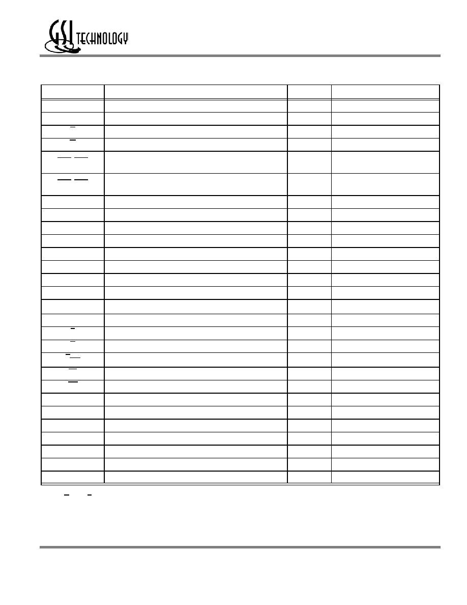
512K x 36 SigmaQuad SRAM -- Top View
1
2
3
4
5
6
7
8
9
10
11
A CQ
V
SS
/SA
(288Mb)
NC/SA
(36Mb)
R/W
BW2
K
BW1
LD
NC/SA
(36Mb)
V
SS
/SA
(144Mb)
CQ
B Q27
Q18
D18
SA
BW3
K
BW0
SA
D17
Q17
Q8
C D27
Q28
D19
V
SS
SA
SA
SA
V
SS
D16
Q7
D8
D D28
D20
Q19
V
SS
V
SS
V
SS
V
SS
V
SS
Q16
D15
D7
E Q29
D29
Q20
V
DDQ
V
SS
V
SS
V
SS
V
DDQ
Q15
D6
Q6
F
Q30
Q21
D21
V
DDQ
V
DD
V
SS
V
DD
V
DDQ
D14
Q14
Q5
G D30
D22
Q22
V
DDQ
V
DD
V
SS
V
DD
V
DDQ
Q13
D13
D5
H D
OFF
V
REF
V
DDQ
V
DDQ
V
DD
V
SS
V
DD
V
DDQ
V
DDQ
V
REF
ZQ
J D31
Q31
D23
V
DDQ
V
DD
V
SS
V
DD
V
DDQ
D12
Q4
D4
K Q32
D32
Q23
V
DDQ
V
DD
V
SS
V
DD
V
DDQ
Q12
D3
Q3
L Q33
Q24
D24
V
DDQ
V
SS
V
SS
V
SS
V
DDQ
D11
Q11
Q2
M D33
Q34
D25
V
SS
V
SS
V
SS
V
SS
V
SS
D10
Q1
D2
N D34
D26
Q25
V
SS
SA
SA
SA
V
SS
Q10
D9
D1
P Q35
D35
Q26
SA
SA
C
SA
SA
Q9
D0
Q0
R TDO
TCK
SA
SA
SA
C
SA
SA
SA
TMS
TDI
11 x 15 Bump BGA--13 x 15 mm2 Body--1 mm Bump Pitch
Notes:
1. Expansion addresses: A9 for 36Mb, A3 for 72Mb, A10 for 144Mb, A2 for 288Mb
2. BW0 controls writes to D0:D8. BW1 controls writes to D9:D17.
3. BW2 controls writes to D18:D26. BW3 controls writes to D27:D35.
4. It is recommended that H1 be tied low for compatibility with future devices.
Rev: 1.01 6/2003
4/30
© 2003, Giga Semiconductor, Inc.
Specifications cited are design targets and are subject to change without notice. For latest documentation contact your GSI representative.
Preliminary
GS8182S18/36D-333/300/250/200/167
Pin Description Table
Symbol
Description
Type
Comments
SA
Synchronous Address Inputs
Input
--
NC
No Connect
--
--
R
Synchronous Read
Input
Active Low
W
Synchronous Write
Input
Active Low
BW0BW1
Synchronous Byte Writes
Input
Active Low
x18 Version
BW0BW3
Synchronous Byte Writes
Input
Active Low
x36 Version
K
Input Clock
Input
Active High
MCH
Must Connect High
Input
DC mode pin
C
Output Clock
Input
Active High
MCH
Must Connect High
Input
DC mode pin
TMS
Test Mode Select
Input
--
TDI
Test Data Input
Input
--
TCK
Test Clock Input
Input
--
TDO
Test Data Output
Output
--
V
REF
HSTL Input Reference Voltage
Input
--
ZQ
Output Impedance Matching Input
Input
--
K
Input Clock
Input
Active Low
C
Output Clock
Output
Active Low
D
OFF
DLL Disable
--
Active Low
LD
Synchronous Load Pin
--
Active Low
CQ
Output Echo Clock
Output
Active Low
CQ
Output Echo Clock
Output
Active High
MCL
Must Connect Low
--
--
DNU
Do Not Use
--
--
D0D35
Synchronous Data Inputs
Input
x36 Version
Q0Q35
Synchronous Data Outputs
Output
x36 Version
D0D17
Synchronous Data Inputs
Input
x18 Version
Q0Q17
Synchronous Data Outputs
Output
x18 Version
Notes:
1. C, C, K, or K cannot be set to V
REF
voltage.
2. When ZQ pin is directly connected to V
DD
, output impedance is set to minimum value and it cannot be connected to ground or left uncon-
nected.
3. NC = Not Connected to die or any other pin
Rev: 1.01 6/2003
5/30
© 2003, Giga Semiconductor, Inc.
Specifications cited are design targets and are subject to change without notice. For latest documentation contact your GSI representative.
Preliminary
GS8182S18/36D-333/300/250/200/167
Background
Separate I/O SRAMs, from a system architecture point of view, are attractive in applications where alternating reads and writes are needed.
Therefore, the SigmaSIO-II SRAM interface and truth table are optimized for alternating reads and writes. Separate I/O SRAMs are unpopular in
applications where multiple reads or multiple writes are needed because burst read or write transfers from Separate I/O SRAMs can cut the
RAM's bandwidth in half.
A SigmaSIO-II SRAM can begin an alternating sequence of reads and writes with either a read or a write. In order for any separate I/O SRAM
that shares a common address between its two ports to keep both ports running all the time, the RAM must implement some sort of burst transfer
protocol. The burst must be at least long enough to cover the time the opposite port is receiving instructions on what to do next. The rate at which
a RAM can accept a new random address is the most fundamental performance metric for the RAM. Each of the three SigmaQuad SRAMs
support similar address rates because random address rate is determined by the internal performance of the RAM and they are all based on the
same internal circuits. Differences between the truth tables of the different SigmaQuad SRAMs, or any other Separate I/O SRAMs, follow from
differences in how the RAM's interface is contrived to interact with the rest of the system. Each mode of operation has its own advantages and
disadvantages. The user should consider the nature of the work to be done by the RAM to evaluate which version is best suited to the application
at hand.
V
DD
Power Supply
Supply
1.8 V Nominal
V
DDQ
Isolated Output Buffer Supply
Supply
1.8 or 1.5 V Nominal
V
SS
Power Supply: Ground
Supply
--
Pin Description Table
Symbol
Description
Type
Comments
Notes:
1. C, C, K, or K cannot be set to V
REF
voltage.
2. When ZQ pin is directly connected to V
DD
, output impedance is set to minimum value and it cannot be connected to ground or left uncon-
nected.
3. NC = Not Connected to die or any other pin