8321ZVxx_r1_01.fm
Rev: 1.01 6/2003
1/32
© 2003, Giga Semiconductor, Inc.
Specifications cited are subject to change without notice. For latest documentation see http://www.gsitechnology.com.
NoBL is a trademark of Cypress Semiconductor Corp.. NtRAM is a trademark of Samsung Electronics Co.. ZBT is a trademark of Integrated Device Technology, Inc.
GS8321ZV18/32/36E-250/225/200/166/150/133
36Mb Pipelined and Flow Through
Synchronous NBT SRAM
250 MHz133 MHz
1.8 V V
DD
1.8 V I/O
165-Bump FP-BGA
Commercial Temp
Industrial Temp
Features
· User-configurable Pipeline and Flow Through mode
· NBT (No Bus Turn Around) functionality allows zero wait
read-write-read bus utilization
· Fully pin-compatible with both pipelined and flow through
NtRAMTM, NoBLTM and ZBTTM SRAMs
· IEEE 1149.1 JTAG-compatible Boundary Scan
· 1.8 V +10%/10% core power supply
· LBO pin for Linear or Interleave Burst mode
· Pin-compatible with 2Mb, 4Mb, 8Mb, and 18Mb devices
· Byte write operation (9-bit Bytes)
· 3 chip enable signals for easy depth expansion
· ZZ pin for automatic power-down
· JEDEC-standard 165-bump FP-BGA package
Functional Description
The GS8321ZV18/32/36E is a 36Mbit Synchronous Static
SRAM. GSI's NBT SRAMs, like ZBT, NtRAM, NoBL or
other pipelined read/double late write or flow through read/
single late write SRAMs, allow utilization of all available bus
bandwidth by eliminating the need to insert deselect cycles
when the device is switched from read to write cycles.
Because it is a synchronous device, address, data inputs, and
read/ write control inputs are captured on the rising edge of the
input clock. Burst order control (LBO) must be tied to a power
rail for proper operation. Asynchronous inputs include the
Sleep mode enable, ZZ and Output Enable. Output Enable can
be used to override the synchronous control of the output
drivers and turn the RAM's output drivers off at any time.
Write cycles are internally self-timed and initiated by the rising
edge of the clock input. This feature eliminates complex off-
chip write pulse generation required by asynchronous SRAMs
and simplifies input signal timing.
The GS8321ZV18/32/36E may be configured by the user to
operate in Pipeline or Flow Through mode. Operating as a
pipelined synchronous device, in addition to the rising-edge-
triggered registers that capture input signals, the device
incorporates a rising-edge-triggered output register. For read
cycles, pipelined SRAM output data is temporarily stored by
the edge triggered output register during the access cycle and
then released to the output drivers at the next rising edge of
clock.
The GS8321ZV18/32/36E is implemented with GSI's high
performance CMOS technology and is available in JEDEC-
standard 165-bump FP-BGA package.
-250 -225 -200 -166 -150 -133 Unit
Pipeline
3-1-1-1
t
KQ
tCycle
2.3
4.0
2.5
4.4
2.7
5.0
2.9
6.0
3.3
6.7
3.5
7.5
ns
ns
Curr
(x18)
Curr
(x36)
285
350
265
320
245
295
220
260
210
240
185
215
mA
mA
Flow
Through
2-1-1-1
t
KQ
tCycle
6.5
6.5
7.0
7.0
7.5
7.5
8.0
8.0
8.5
8.5
8.5
8.5
ns
ns
Curr
(x18)
Curr
(x36)
205
235
195
225
185
210
175
200
165
190
155
175
mA
mA
Rev: 1.01 6/2003
2/32
© 2003, Giga Semiconductor, Inc.
Specifications cited are subject to change without notice. For latest documentation see http://www.gsitechnology.com.
GS8321ZV18/32/36E-250/225/200/166/150/133
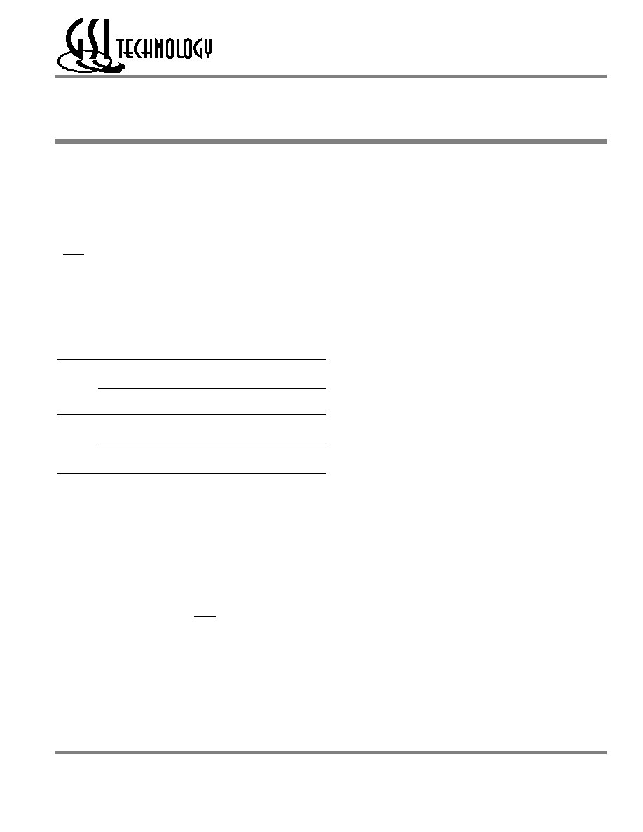
165 Bump BGA--x18 Commom I/O--Top View (Package E)
1
2
3
4
5
6
7
8
9
10
11
A
NC
A
E1
BB
NC
E3
CKE
ADV
A
A
A
A
B
NC
A
E2
NC
BA
CK
W
G
A
A
NC
B
C
NC
NC
V
DDQ
V
SS
V
SS
V
SS
V
SS
V
SS
V
DDQ
NC
DQPA
C
D
NC
DQB
V
DDQ
V
DD
V
SS
V
SS
V
SS
V
DD
V
DDQ
NC
DQA
D
E
NC
DQB
V
DDQ
V
DD
V
SS
V
SS
V
SS
V
DD
V
DDQ
NC
DQA
E
F
NC
DQB
V
DDQ
V
DD
V
SS
V
SS
V
SS
V
DD
V
DDQ
NC
DQA
F
G
NC
DQB
V
DDQ
V
DD
V
SS
V
SS
V
SS
V
DD
V
DDQ
NC
DQA
G
H
FT
MCH
NC
V
DD
V
SS
V
SS
V
SS
V
DD
NC
NC
ZZ
H
J
DQB
NC
V
DDQ
V
DD
V
SS
V
SS
V
SS
V
DD
V
DDQ
DQA
NC
J
K
DQB
NC
V
DDQ
V
DD
V
SS
V
SS
V
SS
V
DD
V
DDQ
DQA
NC
K
L
DQB
NC
V
DDQ
V
DD
V
SS
V
SS
V
SS
V
DD
V
DDQ
DQA
NC
L
M
DQB
NC
V
DDQ
V
DD
V
SS
V
SS
V
SS
V
DD
V
DDQ
DQA
NC
M
N
DQPB
NC
V
DDQ
V
SS
NC
NC
NC
V
SS
V
DDQ
NC
NC
N
P
NC
NC
A
A
TDI
A1
TDO
A
A
A
NC
P
R
LBO
A19
A
A
TMS
A0
TCK
A
A
A
A
R
11 x 15 Bump BGA--15 mm x 17 mm Body--1.0 mm Bump Pitch
Rev: 1.01 6/2003
3/32
© 2003, Giga Semiconductor, Inc.
Specifications cited are subject to change without notice. For latest documentation see http://www.gsitechnology.com.
GS8321ZV18/32/36E-250/225/200/166/150/133
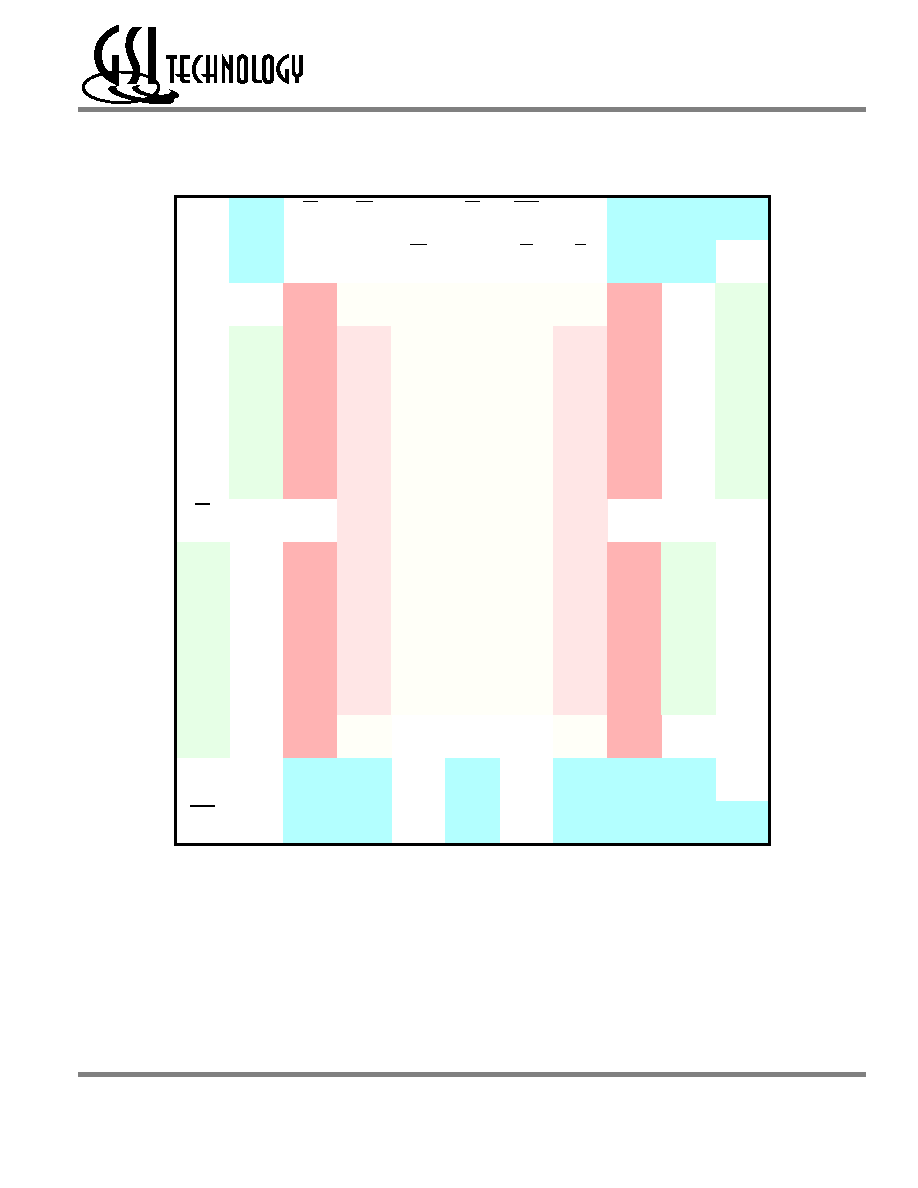
165 Bump BGA--x32 Common I/O--Top View (Package E)
1
2
3
4
5
6
7
8
9
10
11
A
NC
A
E1
BC
BB
E3
CKE
ADV
A
A
NC
A
B
NC
A
E2
BD
BA
CK
W
G
A
A
NC
B
C
NC
NC
V
DDQ
V
SS
V
SS
V
SS
V
SS
V
SS
V
DDQ
NC
NC
C
D
DQC
DQC
V
DDQ
V
DD
V
SS
V
SS
V
SS
V
DD
V
DDQ
DQB
DQB
D
E
DQC
DQC
V
DDQ
V
DD
V
SS
V
SS
V
SS
V
DD
V
DDQ
DQB
DQB
E
F
DQC
DQC
V
DDQ
V
DD
V
SS
V
SS
V
SS
V
DD
V
DDQ
DQB
DQB
F
G
DQC
DQC
V
DDQ
V
DD
V
SS
V
SS
V
SS
V
DD
V
DDQ
DQB
DQB
G
H
FT
MCH
NC
V
DD
V
SS
V
SS
V
SS
V
DD
NC
NC
ZZ
H
J
DQD
DQD
V
DDQ
V
DD
V
SS
V
SS
V
SS
V
DD
V
DDQ
DQA
DQA
J
K
DQD
DQD
V
DDQ
V
DD
V
SS
V
SS
V
SS
V
DD
V
DDQ
DQA
DQA
K
L
DQD
DQD
V
DDQ
V
DD
V
SS
V
SS
V
SS
V
DD
V
DDQ
DQA
DQA
L
M
DQD
DQD
V
DDQ
V
DD
V
SS
V
SS
V
SS
V
DD
V
DDQ
DQA
DQA
M
N
NC
NC
V
DDQ
V
SS
NC
NC
NC
V
SS
V
DDQ
NC
NC
N
P
NC
NC
A
A
TDI
A1
TDO
A
A
A
NC
P
R
LBO
A19
A
A
TMS
A0
TCK
A
A
A
A
R
11 x 15 Bump BGA--15 mm x 17 mm Body--1.0 mm Bump Pitch
Rev: 1.01 6/2003
4/32
© 2003, Giga Semiconductor, Inc.
Specifications cited are subject to change without notice. For latest documentation see http://www.gsitechnology.com.
GS8321ZV18/32/36E-250/225/200/166/150/133
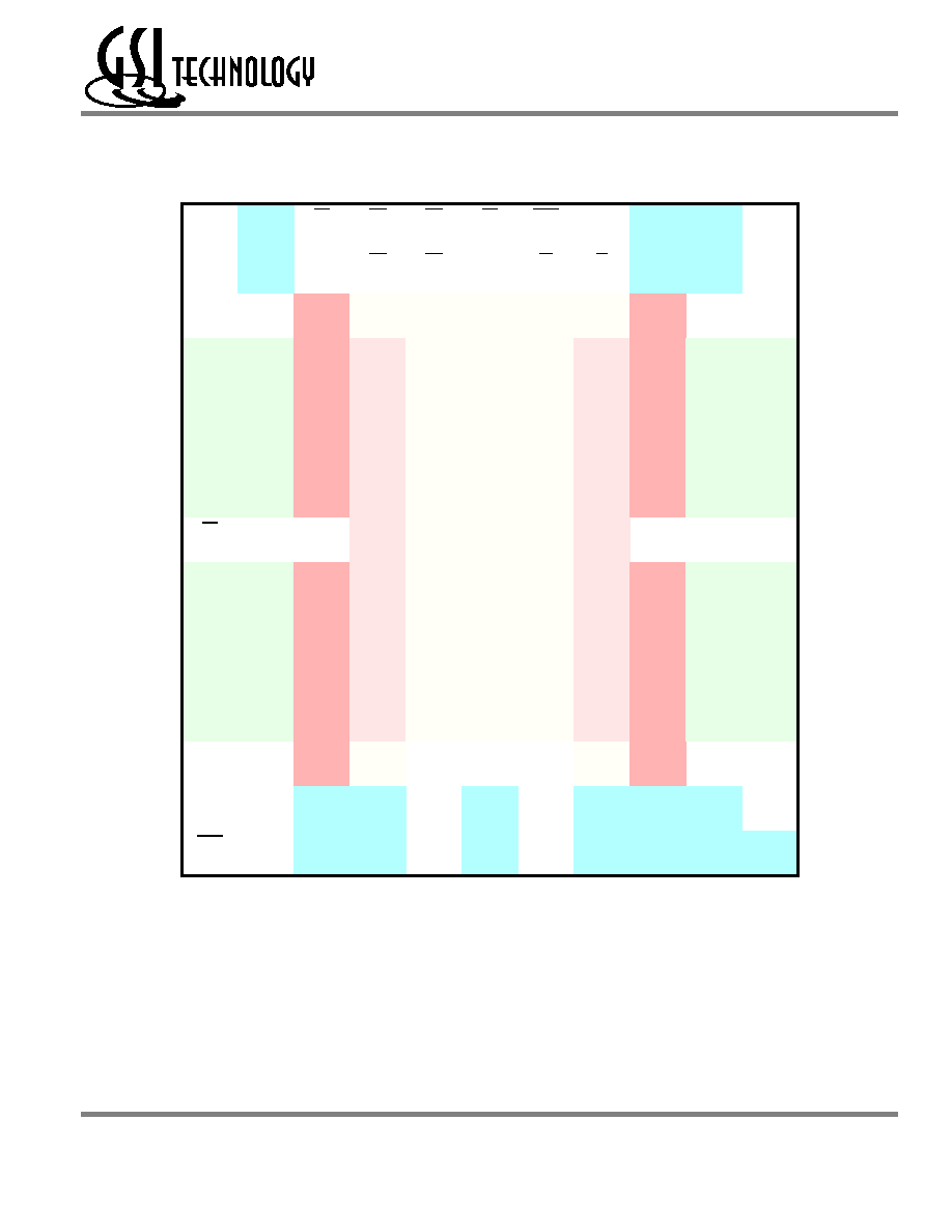
165 Bump BGA--x36 Common I/O--Top View (Package E)
1
2
3
4
5
6
7
8
9
10
11
A
NC
A
E1
BC
BB
E3
CKE
ADV
A
A
NC
A
B
NC
A
E2
BD
BA
CK
W
G
A
A
NC
B
C
DQPC
NC
V
DDQ
V
SS
V
SS
V
SS
V
SS
V
SS
V
DDQ
NC
DQPB
C
D
DQC
DQC
V
DDQ
V
DD
V
SS
V
SS
V
SS
V
DD
V
DDQ
DQB
DQB
D
E
DQC
DQC
V
DDQ
V
DD
V
SS
V
SS
V
SS
V
DD
V
DDQ
DQB
DQB
E
F
DQC
DQC
V
DDQ
V
DD
V
SS
V
SS
V
SS
V
DD
V
DDQ
DQB
DQB
F
G
DQC
DQC
V
DDQ
V
DD
V
SS
V
SS
V
SS
V
DD
V
DDQ
DQB
DQB
G
H
FT
MCH
NC
V
DD
V
SS
V
SS
V
SS
V
DD
NC
NC
ZZ
H
J
DQD
DQD
V
DDQ
V
DD
V
SS
V
SS
V
SS
V
DD
V
DDQ
DQA
DQA
J
K
DQD
DQD
V
DDQ
V
DD
V
SS
V
SS
V
SS
V
DD
V
DDQ
DQA
DQA
K
L
DQD
DQD
V
DDQ
V
DD
V
SS
V
SS
V
SS
V
DD
V
DDQ
DQA
DQA
L
M
DQD
DQD
V
DDQ
V
DD
V
SS
V
SS
V
SS
V
DD
V
DDQ
DQA
DQA
M
N
DQPD
NC
V
DDQ
V
SS
NC
NC
NC
V
SS
V
DDQ
NC
DQPA
N
P
NC
NC
A
A
TDI
A1
TDO
A
A
A
NC
P
R
LBO
A19
A
A
TMS
A0
TCK
A
A
A
A
R
11 x 15 Bump BGA--15 mm x 17 mm Body--1.0 mm Bump Pitch
Rev: 1.01 6/2003
5/32
© 2003, Giga Semiconductor, Inc.
Specifications cited are subject to change without notice. For latest documentation see http://www.gsitechnology.com.
GS8321ZV18/32/36E-250/225/200/166/150/133
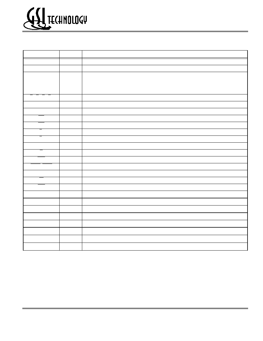
GS832118/32/36E 165-Bump BGA Pin Description
Symbol
Type
Description
A
0
, A
1
I
Address field LSBs and Address Counter Preset Inputs
A
I
Address Inputs
DQ
A
DQ
B
DQ
C
DQ
D
I/O
Data Input and Output pins
B
A
, B
B
, B
C
, B
D
I
Byte Write Enable for DQ
A
, DQ
B
, DQ
C
, DQ
D
I/Os; active low
NC
--
No Connect
CK
I
Clock Input Signal; active high
BW
I
Byte Write--Writes all enabled bytes; active low
GW
I
Global Write Enable--Writes all bytes; active low
E
1
I
Chip Enable; active low
E
3
I
Chip Enable; active low
E
2
I
Chip Enable; active high
G
I
Output Enable; active low
ADV
I
Burst address counter advance enable; active l0w
ADSC, ADSP
I
Address Strobe (Processor, Cache Controller); active low
ZZ
I
Sleep mode control; active high
FT
I
Flow Through or Pipeline mode; active low
LBO
I
Linear Burst Order mode; active low
TMS
I
Scan Test Mode Select
TDI
I
Scan Test Data In
TDO
O
Scan Test Data Out
TCK
I
Scan Test Clock
MCL
--
Must Connect Low
V
DD
I
Core power supply
V
SS
I
I/O and Core Ground
V
DDQ
I
Output driver power supply