Rev: 1.02 6/2003
1/41
© 2001, Giga Semiconductor, Inc.
Specifications cited are subject to change without notice. For latest documentation see http://www.gsitechnology.com.
ByteSafe is a Trademark of Giga Semiconductor, Inc. (GSI Technology).
Product Preview
GS832218(B/E)/GS832236(B/E)/GS832272(C)
2M x 18, 1M x 36, 512K x 72
36Mb S/DCD Sync Burst SRAMs
250 MHz133MHz
2.5 V or 3.3 V V
DD
2.5 V or 3.3 V I/O
119-, 165-, & 209-Pin BGA
Commercial Temp
Industrial Temp
Features
· FT pin for user-configurable flow through or pipeline operation
· Single/Dual Cycle Deselect selectable
· IEEE 1149.1 JTAG-compatible Boundary Scan
· ZQ mode pin for user-selectable high/low output drive
· 2.5 V +10%/10% core power supply
· 3.3 V +10%/10% core power supply
· 2.5 V or 3.3 V I/O supply
· LBO pin for Linear or Interleaved Burst mode
· Internal input resistors on mode pins allow floating mode pins
· Default to SCD x18/x36 Interleaved Pipeline mode
· Byte Write (BW) and/or Global Write (GW) operation
· Internal self-timed write cycle
· Automatic power-down for portable applications
· JEDEC-standard 119-, 165-, and 209-bump BGA package
Functional Description
Applications
The GS832218/36/72 is a
37,748,736-bit high performance
synchronous SRAM with a 2-bit burst address counter. Although
of a type originally developed for Level 2 Cache applications
supporting high performance CPUs, the device now finds
application in synchronous SRAM applications, ranging from
DSP main store to networking chip set support.
Controls
Addresses, data I/Os, chip enable (E1), address burst control
inputs (ADSP, ADSC, ADV), and write control inputs (Bx, BW,
GW) are synchronous and are controlled by a positive-edge-
triggered clock input (CK). Output enable (G) and power down
control (ZZ) are asynchronous inputs. Burst cycles can be initiated
with either ADSP or ADSC inputs. In Burst mode, subsequent
burst addresses are generated internally and are controlled by
ADV. The burst address counter may be configured to count in
either linear or interleave order with the Linear Burst Order (LBO)
input. The Burst function need not be used. New addresses can be
loaded on every cycle with no degradation of chip performance.
Flow Through/Pipeline Reads
The function of the Data Output register can be controlled by the
user via the FT mode . Holding the FT mode pin low places the
RAM in Flow Through mode, causing output data to bypass the
Data Output Register. Holding FT high places the RAM in
Pipeline mode, activating the rising-edge-triggered Data Output
Register.
SCD and DCD Pipelined Reads
The GS832218/36/72 is a SCD (Single Cycle Deselect) and DCD
(Dual Cycle Deselect) pipelined synchronous SRAM. DCD
SRAMs pipeline disable commands to the same degree as read
commands. SCD SRAMs pipeline deselect commands one stage
less than read commands. SCD RAMs begin turning off their
outputs immediately after the deselect command has been
captured in the input registers. DCD RAMs hold the deselect
command for one full cycle and then begin turning off their
outputs just after the second rising edge of clock. The user may
configure this SRAM for either mode of operation using the SCD
mode input.
Byte Write and Global Write
Byte write operation is performed by using Byte Write enable
(BW) input combined with one or more individual byte write
signals (Bx). In addition, Global Write (GW) is available for
writing all bytes at one time, regardless of the Byte Write control
inputs.
FLXDriveTM
The ZQ pin allows selection between high drive strength (ZQ low)
for multi-drop bus applications and normal drive strength (ZQ
floating or high) point-to-point applications. See the Output Driver
Characteristics chart for details.
Sleep Mode
Low power (Sleep mode) is attained through the assertion (High)
of the ZZ signal, or by stopping the clock (CK). Memory data is
retained during Sleep mode.
Core and Interface Voltages
The GS832218/36/72 operates on a 2.5 V or 3.3 V power supply.
All input are 3.3 V and 2.5 V compatible. Separate output power
(V
DDQ
) pins are used to decouple output noise from the internal
circuits and are 3.3 V and 2.5 V compatible.
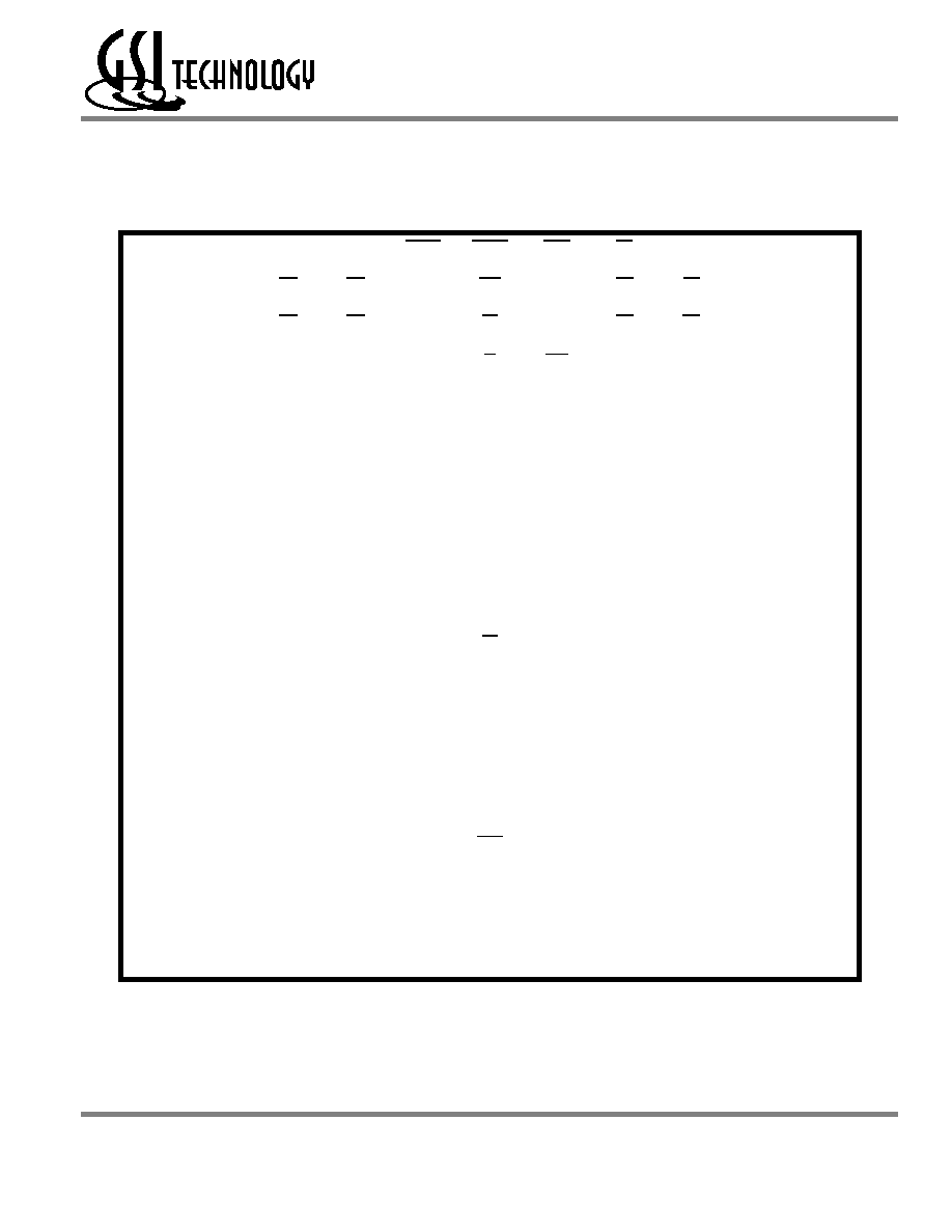
-250 -225 -200 -166 -150 -133 Unit
Pipeline
3-1-1-1
t
KQ(x18/x36)
t
KQ(x72)
tCycle
2.5
3.0
4.0
2.7
3.0
4.4
3.0
3.0
5.0
3.5
3.5
6.0
3.8
3.8
6.7
4.0
4.0
7.5
ns
ns
ns
Curr
(x18)
Curr
(x36)
Curr
(x72)
285
350
440
265
320
410
245
295
370
220
260
320
210
240
300
185
215
265
mA
mA
mA
Flow
Through
2-1-1-1
t
KQ
tCycle
6.5
6.5
7.0
7.0
7.5
7.5
8.0
8.0
8.5
8.5
8.5
8.5
ns
ns
Curr
(x18)
Curr
(x36)
Curr
(x72)
205
235
315
195
225
295
185
210
265
175
200
255
165
190
240
155
175
230
mA
mA
mA
Rev: 1.02 6/2003
3/41
© 2001, Giga Semiconductor, Inc.
Specifications cited are subject to change without notice. For latest documentation see http://www.gsitechnology.com.
Product Preview
GS832218(B/E)/GS832236(B/E)/GS832272(C)
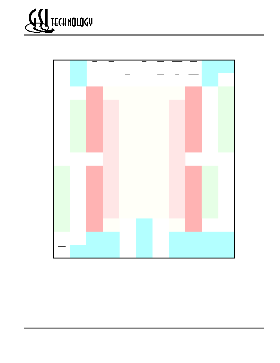
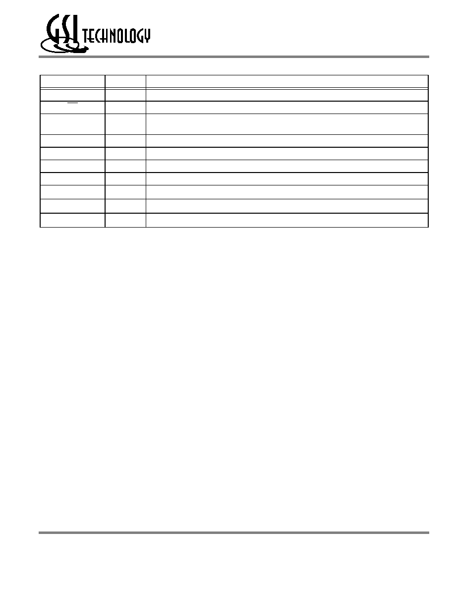
GS832272 209-Bump BGA Pin Description
Symbol
Type
Description
A
0
, A
1
I
Address field LSBs and Address Counter Preset Inputs.
An
I
Address Inputs
DQ
A
DQ
B
DQ
C
DQ
D
DQ
E
DQ
F
DQ
G
DQ
H
I/O
Data Input and Output pins
B
A
, B
B
I
Byte Write Enable for DQ
A
, DQ
B
I/Os; active low
B
C
,B
D
I
Byte Write Enable for DQ
C
, DQ
D
I/Os; active low
B
E
, B
F
, B
G
,B
H
I
Byte Write Enable for DQ
E
, DQ
F
, DQ
G
, DQ
H
I/Os; active low
NC
--
No Connect
CK
I
Clock Input Signal; active high
GW
I
Global Write Enable--Writes all bytes; active low
E
1
I
Chip Enable; active low
E
3
I
Chip Enable; active low
E
2
I
Chip Enable; active high
G
I
Output Enable; active low
ADV
I
Burst address counter advance enable; active low
ADSP, ADSC
I
Address Strobe (Processor, Cache Controller); active low
ZZ
I
Sleep Mode control; active high
FT
I
Flow Through or Pipeline mode; active low
LBO
I
Linear Burst Order mode; active low
SCD
I
Single Cycle Deselect/Dual Cycle Deselect Mode Control
MCH
I
Must Connect High
Rev: 1.02 6/2003
4/41
© 2001, Giga Semiconductor, Inc.
Specifications cited are subject to change without notice. For latest documentation see http://www.gsitechnology.com.
Product Preview
GS832218(B/E)/GS832236(B/E)/GS832272(C)
MCL
Must Connect Low
BW
I
Byte Enable; active low
ZQ
I
FLXDrive Output Impedance Control
(Low = Low Impedance [High Drive], High = High Impedance [Low Drive])
TMS
I
Scan Test Mode Select
TDI
I
Scan Test Data In
TDO
O
Scan Test Data Out
TCK
I
Scan Test Clock
V
DD
I
Core power supply
V
SS
I
I/O and Core Ground
V
DDQ
I
Output driver power supply
GS832272 209-Bump BGA Pin Description
Symbol
Type
Description