Preliminary
GS8342S08/09/18/36E-333/300/250/200/167
36Mb Burst of 2
DDR SigmaSIO-II SRAM
167 MHz333 MHz
1.8 V V
DD
1.8 V and 1.5 V I/O
165-Bump BGA
Commercial Temp
Industrial Temp
Rev: 1.02 8/2005
1/39
© 2003, GSI Technology
Specifications cited are subject to change without notice. For latest documentation see http://www.gsitechnology.com.
Features
· Simultaneous Read and Write SigmaSIOTM Interface
· JEDEC-standard pinout and package
· Dual Double Data Rate interface
· Byte Write controls sampled at data-in time
· DLL circuitry for wide output data valid window and future
frequency scaling
· Burst of 2 Read and Write
· 1.8 V +100/100 mV core power supply
· 1.5 V or 1.8 V HSTL Interface
· Pipelined read operation
· Fully coherent read and write pipelines
· ZQ mode pin for programmable output drive strength
· IEEE 1149.1 JTAG-compliant Boundary Scan
· 165-bump, 15 mm x 17 mm, 1 mm bump pitch BGA package
· RoHS-compliant 165-bump BGA package available
· Pin-compatible with future 72Mb and 144Mb devices
SigmaRAMTM Family Overview
GS8342S08/09/18/36 are built in compliance with the
SigmaSIO-II SRAM pinout standard for Separate I/O
synchronous SRAMs. They are 37,748,736-bit (36Mb)
SRAMs. These are the first in a family of wide, very low
voltage HSTL I/O SRAMs designed to operate at the speeds
needed to implement economical high performance
networking systems.
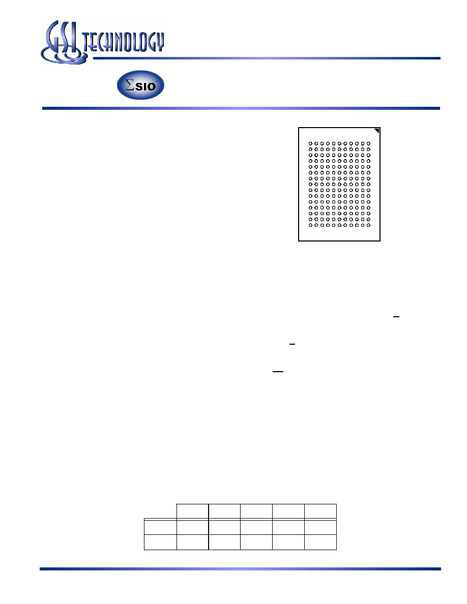
165-Bump, 15 mm x 17 mm BGA
1 mm Bump Pitch, 11 x 15 Bump Array
Bottom View
JEDEC Std. MO-216, Variation CAB-1
Clocking and Addressing Schemes
A Burst of 2
SigmaSIO-II SRAM is a synchronous device. It
employs dual input register clock inputs, K and K. The device
also allows the user to manipulate the output register clock
input quasi independently with dual output register clock
inputs, C and C. If the C clocks are tied high, the K clocks are
routed internally to fire the output registers instead. Each Burst
of 2
SigmaSIO-II SRAM also supplies Echo Clock outputs,
CQ and CQ, which are synchronized with read data output.
When used in a source synchronous clocking scheme, the Echo
Clock outputs can be used to fire input registers at the data's
destination.
Because Separate I/O Burst of 2 RAMs always transfer data in
two packets, A0 is internally set to 0 for the first read or write
transfer, and automatically incremented by 1 for the next
transfer. Because the LSB is tied off internally, the address
field of a Burst of 2 RAM is always one address pin less than
the advertised index depth (e.g., the 2M x 18 has a 1M
addressable index).
Parameter Synopsis
- 333
-300
-250
-200
-167
tKHKH
3.0 ns
3.3 ns
4.0 ns
5.0 ns
6.0 ns
tKHQV
0.45 ns
0.45 ns
0.45 ns
0.45 ns
0.5 ns

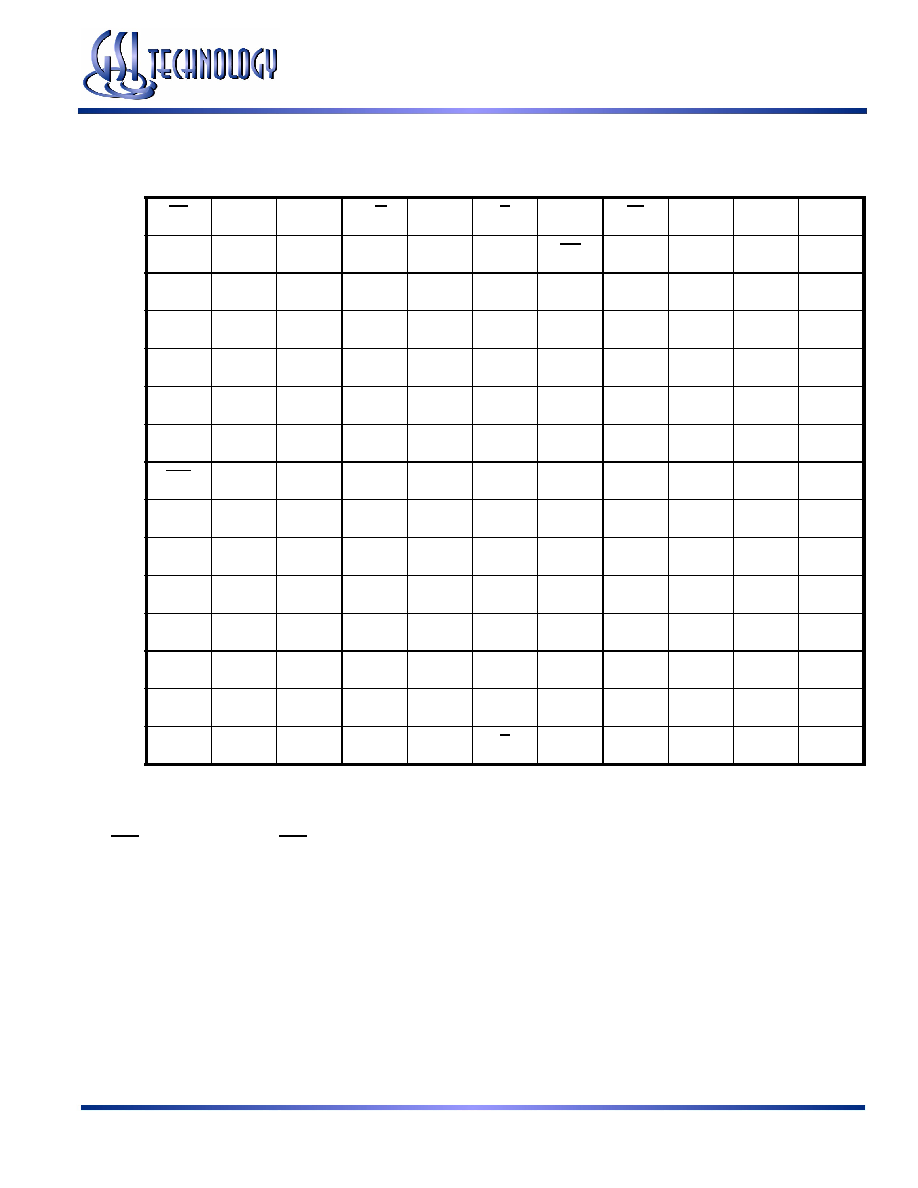
4M x 8 SigmaQuad SRAM--Top View
1
2
3
4
5
6
7
8
9
10
11
A
CQ
V
SS
/SA
(72Mb)
SA
R/W
NW1
K
NC
LD
SA
SA
CQ
B
NC
NC
NC
SA
NC
K
NW0
SA
NC
NC
Q3
C
NC
NC
NC
V
SS
SA
SA
SA
V
SS
NC
NC
D3
D
NC
D4
NC
V
SS
V
SS
V
SS
V
SS
V
SS
NC
NC
NC
E
NC
NC
Q4
V
DDQ
V
SS
V
SS
V
SS
V
DDQ
NC
D2
Q2
F
NC
NC
NC
V
DDQ
V
DD
V
SS
V
DD
V
DDQ
NC
NC
NC
G
NC
D5
Q5
V
DDQ
V
DD
V
SS
V
DD
V
DDQ
NC
NC
NC
H
D
OFF
V
REF
V
DDQ
V
DDQ
V
DD
V
SS
V
DD
V
DDQ
V
DDQ
V
REF
ZQ
J
NC
NC
NC
V
DDQ
V
DD
V
SS
V
DD
V
DDQ
NC
Q1
D1
K
NC
NC
NC
V
DDQ
V
DD
V
SS
V
DD
V
DDQ
NC
NC
NC
L
NC
Q6
D6
V
DDQ
V
SS
V
SS
V
SS
V
DDQ
NC
NC
Q0
M
NC
NC
NC
V
SS
V
SS
V
SS
V
SS
V
SS
NC
NC
D0
N
NC
D7
NC
V
SS
SA
SA
SA
V
SS
NC
NC
NC
P
NC
NC
Q7
SA
SA
C
SA
SA
NC
NC
NC
R
TDO
TCK
SA
SA
SA
C
SA
SA
SA
TMS
TDI
11 x 15 Bump BGA--15 x 17 mm
2
Body--1 mm Bump Pitch
Notes:
1. Expansion addresses: A2 for 72Mb
2. NW0 controls writes to D0:D3. NW1 controls writes to D4:D7.
3. It is recommended that H1 be tied low for compatibility with future devices.
Preliminary
GS8342S08/09/18/36E-333/300/250/200/167
Specifications cited are subject to change without notice. For latest documentation see http://www.gsitechnology.com.
Rev: 1.02 8/2005
2/39
© 2003, GSI Technology
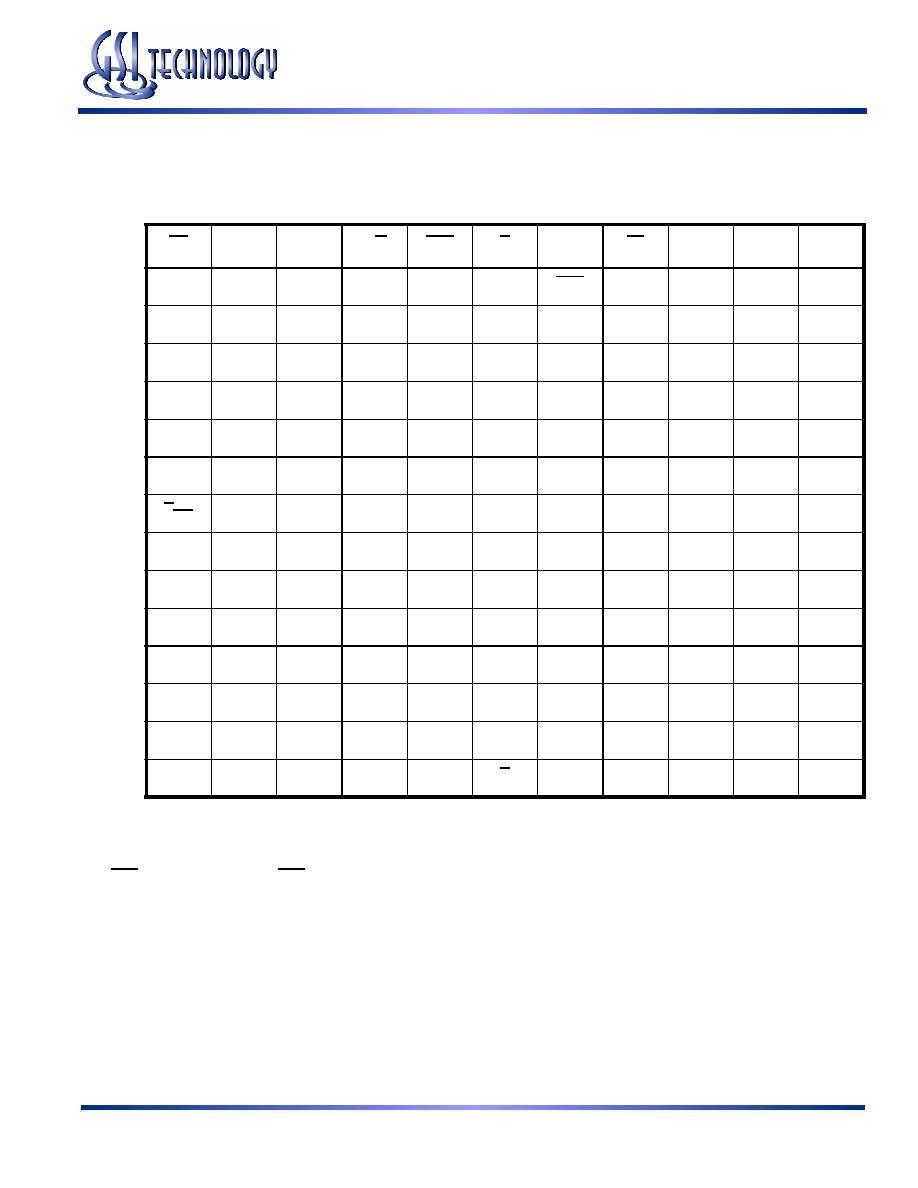
4M x 9 SigmaQuad SRAM--Top View
1
2
3
4
5
6
7
8
9
10
11
A
CQ
V
SS
SA
R/W
NC
K
NC
LD
SA
SA
CQ
B
NC
NC
NC
SA
NC
K
BW
SA
NC
NC
Q4
C
NC
NC
NC
V
SS
SA
SA
SA
V
SS
NC
NC
D4
D
NC
D5
NC
V
SS
V
SS
V
SS
V
SS
V
SS
NC
NC
NC
E
NC
NC
Q5
V
DDQ
V
SS
V
SS
V
SS
V
DDQ
NC
D3
Q3
F
NC
NC
NC
V
DDQ
V
DD
V
SS
V
DD
V
DDQ
NC
NC
NC
G
NC
D6
Q6
V
DDQ
V
DD
V
SS
V
DD
V
DDQ
NC
NC
NC
H
Doff
V
REF
V
DDQ
V
DDQ
V
DD
V
SS
V
DD
V
DDQ
V
DDQ
V
REF
ZQ
J
NC
NC
NC
V
DDQ
V
DD
V
SS
V
DD
V
DDQ
NC
Q2
D2
K
NC
NC
NC
V
DDQ
V
DD
V
SS
V
DD
V
DDQ
NC
NC
NC
L
NC
Q7
D7
V
DDQ
V
SS
V
SS
V
SS
V
DDQ
NC
NC
Q1
M
NC
NC
NC
V
SS
V
SS
V
SS
V
SS
V
SS
NC
NC
D1
N
NC
D8
NC
V
SS
SA
SA
SA
V
SS
NC
NC
NC
P
NC
NC
Q8
SA
SA
C
SA
SA
NC
D0
NC
R
TDO
TCK
SA
SA
SA
C
SA
SA
SA
TMS
TDI
11 x 15 Bump BGA--15 x 17 mm
2
Body--1 mm Bump Pitch
Notes:
4. Expansion addresses: A2 for 72Mb
5. NW0 controls writes to D0:D3. NW1 controls writes to D4:D7.
6. It is recommended that H1 be tied low for compatibility with future devices.
Preliminary
GS8342S08/09/18/36E-333/300/250/200/167
Specifications cited are subject to change without notice. For latest documentation see http://www.gsitechnology.com.
Rev: 1.02 8/2005
3/39
© 2003, GSI Technology
2M x 18 SigmaQuad SRAM--Top View
1
2
3
4
5
6
7
8
9
10
11
A
CQ
V
SS
/SA
(144Mb)
SA
R/W
BW1
K
NC
LD
SA
V
SS
/SA
(72Mb)
CQ
B
NC
Q9
D9
SA
NC
K
BW0
SA
NC
NC
Q8
C
NC
NC
D10
V
SS
SA
SA
SA
V
SS
NC
Q7
D8
D
NC
D11
Q10
V
SS
V
SS
V
SS
V
SS
V
SS
NC
NC
D7
E
NC
NC
Q11
V
DDQ
V
SS
V
SS
V
SS
V
DDQ
NC
D6
Q6
F
NC
Q12
D12
V
DDQ
V
DD
V
SS
V
DD
V
DDQ
NC
NC
Q5
G
NC
D13
Q13
V
DDQ
V
DD
V
SS
V
DD
V
DDQ
NC
NC
D5
H
D
OFF
V
REF
V
DDQ
V
DDQ
V
DD
V
SS
V
DD
V
DDQ
V
DDQ
V
REF
ZQ
J
NC
NC
D14
V
DDQ
V
DD
V
SS
V
DD
V
DDQ
NC
Q4
D4
K
NC
NC
Q14
V
DDQ
V
DD
V
SS
V
DD
V
DDQ
NC
D3
Q3
L
NC
Q15
D15
V
DDQ
V
SS
V
SS
V
SS
V
DDQ
NC
NC
Q2
M
NC
NC
D16
V
SS
V
SS
V
SS
V
SS
V
SS
NC
Q1
D2
N
NC
D17
Q16
V
SS
SA
SA
SA
V
SS
NC
NC
D1
P
NC
NC
Q17
SA
SA
C
SA
SA
NC
D0
Q0
R
TDO
TCK
SA
SA
SA
C
SA
SA
SA
TMS
TDI
11 x 15 Bump BGA--15 x 17 mm
2
Body--1 mm Bump Pitch
Notes:
1. Expansion addresses: A10 for 72Mb, A2 for 144Mb
2. BW0 controls writes to D0:D8. BW1 controls writes to D9:D17.
3. It is recommended that H1 be tied low for compatibility with future devices.
Preliminary
GS8342S08/09/18/36E-333/300/250/200/167
Specifications cited are subject to change without notice. For latest documentation see http://www.gsitechnology.com.
Rev: 1.02 8/2005
4/39
© 2003, GSI Technology

1M x 36 SigmaQuad SRAM--Top View
1
2
3
4
5
6
7
8
9
10
11
A
CQ
V
SS
/SA
(288Mb)
NC/SA
(72Mb)
R/W
BW2
K
BW1
LD
SA
V
SS
/SA
(144Mb)
CQ
B
Q27
Q18
D18
SA
BW3
K
BW0
SA
D17
Q17
Q8
C
D27
Q28
D19
V
SS
SA
SA
SA
V
SS
D16
Q7
D8
D
D28
D20
Q19
V
SS
V
SS
V
SS
V
SS
V
SS
Q16
D15
D7
E
Q29
D29
Q20
V
DDQ
V
SS
V
SS
V
SS
V
DDQ
Q15
D6
Q6
F
Q30
Q21
D21
V
DDQ
V
DD
V
SS
V
DD
V
DDQ
D14
Q14
Q5
G
D30
D22
Q22
V
DDQ
V
DD
V
SS
V
DD
V
DDQ
Q13
D13
D5
H
D
OFF
V
REF
V
DDQ
V
DDQ
V
DD
V
SS
V
DD
V
DDQ
V
DDQ
V
REF
ZQ
J
D31
Q31
D23
V
DDQ
V
DD
V
SS
V
DD
V
DDQ
D12
Q4
D4
K
Q32
D32
Q23
V
DDQ
V
DD
V
SS
V
DD
V
DDQ
Q12
D3
Q3
L
Q33
Q24
D24
V
DDQ
V
SS
V
SS
V
SS
V
DDQ
D11
Q11
Q2
M
D33
Q34
D25
V
SS
V
SS
V
SS
V
SS
V
SS
D10
Q1
D2
N
D34
D26
Q25
V
SS
SA
SA
SA
V
SS
Q10
D9
D1
P
Q35
D35
Q26
SA
SA
C
SA
SA
Q9
D0
Q0
R
TDO
TCK
SA
SA
SA
C
SA
SA
SA
TMS
TDI
11 x 15 Bump BGA--15 x 17 mm
2
Body--1 mm Bump Pitch
Notes:
1. Expansion addresses: A3 for 72Mb, A10 for 144Mb, A2 for 288Mb
2. BW0 controls writes to D0:D8. BW1 controls writes to D9:D17.
3. BW2 controls writes to D18:D26. BW3 controls writes to D27:D35.
4. It is recommended that H1 be tied low for compatibility with future devices.
Preliminary
GS8342S08/09/18/36E-333/300/250/200/167
Specifications cited are subject to change without notice. For latest documentation see http://www.gsitechnology.com.
Rev: 1.02 8/2005
5/39
© 2003, GSI Technology