Preliminary
GS8662R08/09/18/36E-333/300/250/200/167
72Mb SigmaCIO DDR-II
Burst of 4 SRAM
333 MHz167 MHz
1.8 V V
DD
1.8 V and 1.5 V I/O
165-Bump BGA
Commercial Temp
Industrial Temp
Rev: 1.01 9/2005
1/37
© 2005, GSI Technology
Specifications cited are subject to change without notice. For latest documentation see http://www.gsitechnology.com.
Features
· Simultaneous Read and Write SigmaCIOTM Interface
· Common I/O bus
· JEDEC-standard pinout and package
· Double Data Rate interface
· Byte Write (x36 and x18) and Nybble Write (x8) function
· Burst of 4 Read and Write
· 1.8 V +100/100 mV core power supply
· 1.5 V or 1.8 V HSTL Interface
· Pipelined read operation with self-timed Late Write
· Fully coherent read and write pipelines
· ZQ pin for programmable output drive strength
· IEEE 1149.1 JTAG-compliant Boundary Scan
· Pin-compatible with present 9Mb, 18Mb, 36Mb and future
144Mb devices
· 165-bump, 15 mm x 17 mm, 1 mm bump pitch BGA package
· RoHS-compliant 165-bump BGA package available
SigmaCIOTM Family Overview
The GS8662R08/09/18/36E are built in compliance with the
SigmaCIO DDR-II SRAM pinout standard for Common I/O
synchronous SRAMs. They are 75,497,472-bit (72Mb)
SRAMs. The GS8662R08/09/18/36E SigmaCIO SRAMs are
just one element in a family of low power, low voltage HSTL
I/O SRAMs designed to operate at the speeds needed to
implement economical high performance networking systems.
Clocking and Addressing Schemes
The GS8662R08/09/18/36E SigmaCIO DDR-II SRAMs are
synchronous devices. They employ two input register clock
inputs, K and K. K and K are independent single-ended clock
inputs, not differential inputs to a single differential clock input
buffer. The device also allows the user to manipulate the
output register clock inputs quasi independently with the C and
C clock inputs. C and C are also independent single-ended
clock inputs, not differential inputs. If the C clocks are tied
high, the K clocks are routed internally to fire the output
registers instead.
Common I/O x36 and x18 SigmaCIO DDR-II B4
RAMs
always transfer data in four packets. When a new address is
loaded, A0 and A1 preset an internal 2 bit linear address
counter. The counter increments by 1 for each beat of a burst of
four data transfer. The counter always wraps to 00 after
reaching 11, no matter where it starts.
Common I/O x8 SigmaCIO DDR-II B4 RAMs always transfer
data in four packets. When a new address is loaded, the LSBs
are internally set to 0 for the first read or write transfer, and
incremented by 1 for the next 3 transfers. Because the LSBs
are tied off internally, the address field of a x8 SigmaCIO
DDR-II B4 RAM is always two address pins less than the
advertised index depth (e.g., the 4M x 18 has a 1024K
addressable index).
Parameter Synopsis
-333
-300
-250
-200
-167
tKHKH
3.0 ns
3.3 ns
4.0 ns
5.0 ns
6.0 ns
tKHQV
0.45 ns
0.45 ns
0.45 ns
0.45 ns
0.5 ns
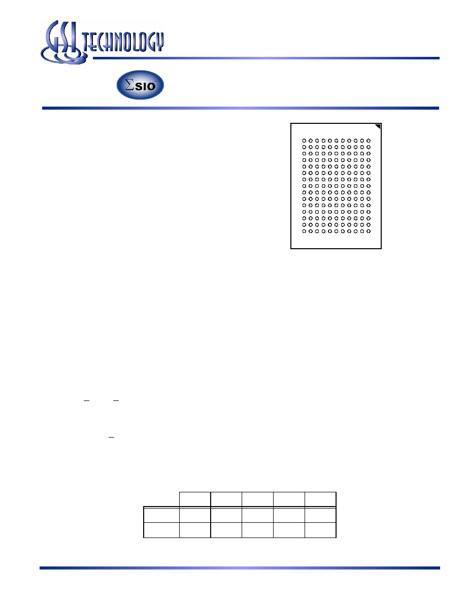
165-Bump, 15 mm x 17 mm BGA
1 mm Bump Pitch, 11 x 15 Bump Array
Bottom View
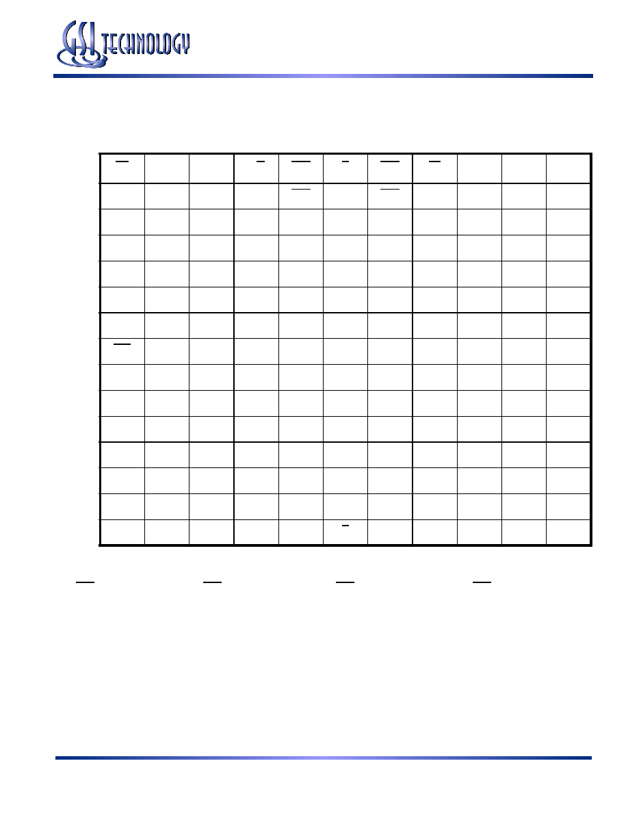
2M x 36 SigmaCIO DDR-II SRAM--Top View
1
2
3
4
5
6
7
8
9
10
11
A
CQ
MCL/SA
(144Mb)
SA
R/W
BW2
K
BW1
LD
SA
SA
CQ
B
NC
DQ27
DQ18
SA
BW3
K
BW0
SA
NC
NC
DQ8
C
NC
NC
DQ28
V
SS
SA
SA0
SA1
V
SS
NC
DQ17
DQ7
D
NC
DQ29
DQ19
V
SS
V
SS
V
SS
V
SS
V
SS
NC
NC
DQ16
E
NC
NC
DQ20
V
DDQ
V
SS
V
SS
V
SS
V
DDQ
NC
DQ15
DQ6
F
NC
DQ30
DQ21
V
DDQ
V
DD
V
SS
V
DD
V
DDQ
NC
NC
DQ5
G
NC
DQ31
DQ22
V
DDQ
V
DD
V
SS
V
DD
V
DDQ
NC
NC
DQ14
H
Doff
V
REF
V
DDQ
V
DDQ
V
DD
V
SS
V
DD
V
DDQ
V
DDQ
V
REF
ZQ
J
NC
NC
DQ32
V
DDQ
V
DD
V
SS
V
DD
V
DDQ
NC
DQ13
DQ4
K
NC
NC
DQ23
V
DDQ
V
DD
V
SS
V
DD
V
DDQ
NC
DQ12
DQ3
L
NC
DQ33
DQ24
V
DDQ
V
SS
V
SS
V
SS
V
DDQ
NC
NC
DQ2
M
NC
NC
DQ34
V
SS
V
SS
V
SS
V
SS
V
SS
NC
DQ11
DQ1
N
NC
DQ35
DQ25
V
SS
SA
SA
SA
V
SS
NC
NC
DQ10
P
NC
NC
DQ26
SA
SA
C
SA
SA
NC
DQ9
DQ0
R
TDO
TCK
SA
SA
SA
C
SA
SA
SA
TMS
TDI
11 x 15 Bump BGA--13 x 15 mm
2
Body--1 mm Bump Pitch
Notes:
1. BW0 controls writes to DQ0:DQ8; BW1 controls writes to DQ9:DQ17; BW2 controls writes to DQ18:DQ26; BW3 controls writes to
DQ27:DQ35
2. MCL = Must Connect Low
Preliminary
GS8662R08/09/18/36E-333/300/250/200/167
Specifications cited are subject to change without notice. For latest documentation see http://www.gsitechnology.com.
Rev: 1.01 9/2005
2/37
© 2005, GSI Technology

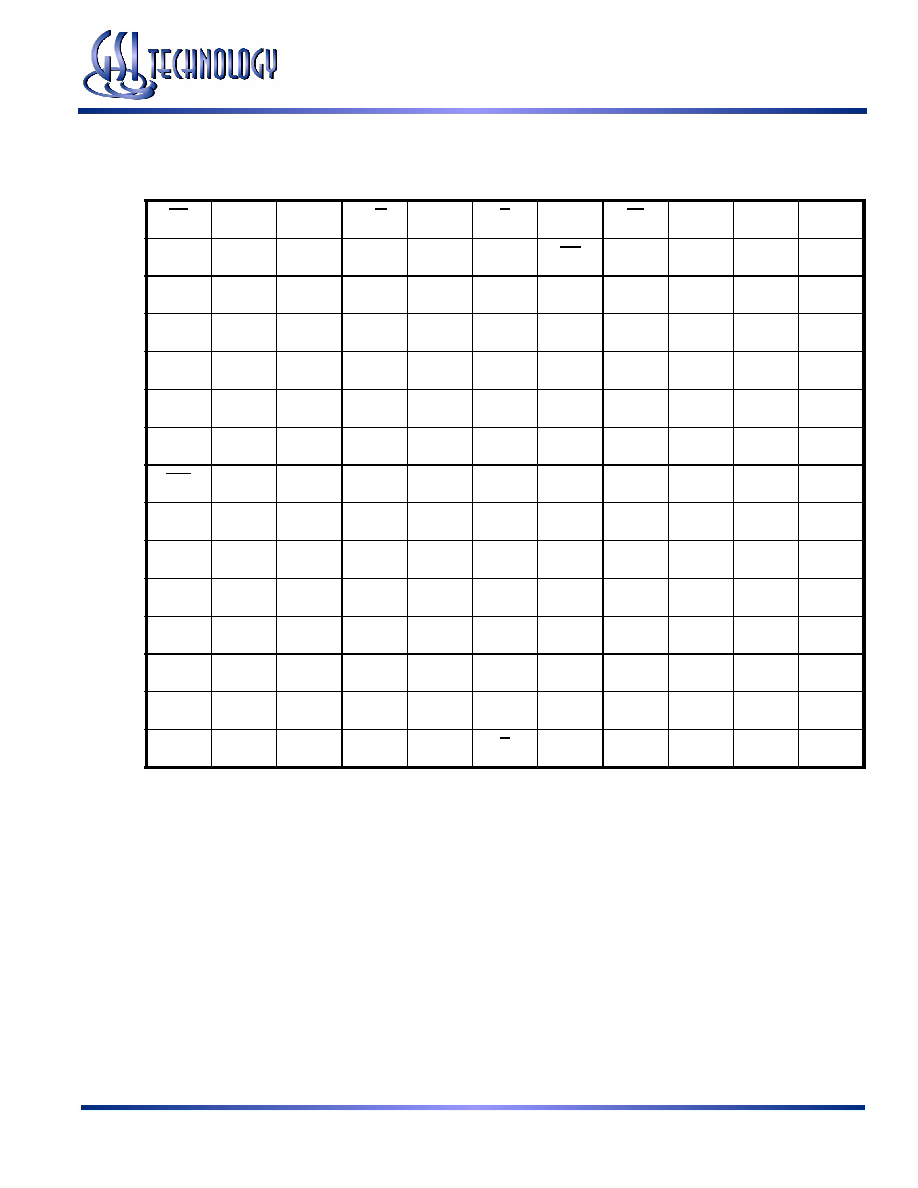
4M x 18 SigmaCIO DDR-II SRAM--Top View
1
2
3
4
5
6
7
8
9
10
11
A
CQ
SA
SA
R/W
BW1
K
NC
LD
SA
SA
CQ
B
NC
DQ9
NC
SA
NC
K
BW0
SA
NC
NC
DQ8
C
NC
NC
NC
V
SS
SA
SA0
SA1
V
SS
NC
DQ7
NC
D
NC
NC
DQ10
V
SS
V
SS
V
SS
V
SS
V
SS
NC
NC
NC
E
NC
NC
DQ11
V
DDQ
V
SS
V
SS
V
SS
V
DDQ
NC
NC
DQ6
F
NC
DQ12
NC
V
DDQ
V
DD
V
SS
V
DD
V
DDQ
NC
NC
DQ5
G
NC
NC
DQ13
V
DDQ
V
DD
V
SS
V
DD
V
DDQ
NC
NC
NC
H
Doff
V
REF
V
DDQ
V
DDQ
V
DD
V
SS
V
DD
V
DDQ
V
DDQ
V
REF
ZQ
J
NC
NC
NC
V
DDQ
V
DD
V
SS
V
DD
V
DDQ
NC
DQ4
NC
K
NC
NC
DQ14
V
DDQ
V
DD
V
SS
V
DD
V
DDQ
NC
NC
DQ3
L
NC
DQ15
NC
V
DDQ
V
SS
V
SS
V
SS
V
DDQ
NC
NC
DQ2
M
NC
NC
NC
V
SS
V
SS
V
SS
V
SS
V
SS
NC
DQ1
NC
N
NC
NC
DQ16
V
SS
SA
SA
SA
V
SS
NC
NC
NC
P
NC
NC
DQ17
SA
SA
C
SA
SA
NC
NC
DQ0
R
TDO
TCK
SA
SA
SA
C
SA
SA
SA
TMS
TDI
11 x 15 Bump BGA--13 x 15 mm
2
Body--1 mm Bump Pitch
Notes:
1. BW0 controls writes to DQ0:DQ8; BW1 controls writes to DQ9:DQ17
2. MCL = Must Connect Low
Preliminary
GS8662R08/09/18/36E-333/300/250/200/167
Specifications cited are subject to change without notice. For latest documentation see http://www.gsitechnology.com.
Rev: 1.01 9/2005
3/37
© 2005, GSI Technology
8M x 9 SigmaCIO DDR-II SRAM--Top View
1
2
3
4
5
6
7
8
9
10
11
A
CQ
SA
SA
R/W
NC
K
NC
LD
SA
SA
CQ
B
NC
NC
NC
SA
NC
K
BW
SA
NC
NC
DQ4
C
NC
NC
NC
V
SS
SA
NC
SA
V
SS
NC
NC
NC
D
NC
NC
NC
V
SS
V
SS
V
SS
V
SS
V
SS
NC
NC
NC
E
NC
NC
DQ5
V
DDQ
V
SS
V
SS
V
SS
V
DDQ
NC
NC
DQ3
F
NC
NC
NC
V
DDQ
V
DD
V
SS
V
DD
V
DDQ
NC
NC
NC
G
NC
NC
DQ6
V
DDQ
V
DD
V
SS
V
DD
V
DDQ
NC
NC
NC
H
Doff
V
REF
V
DDQ
V
DDQ
V
DD
V
SS
V
DD
V
DDQ
V
DDQ
V
REF
ZQ
J
NC
NC
NC
V
DDQ
V
DD
V
SS
V
DD
V
DDQ
NC
DQ2
NC
K
NC
NC
NC
V
DDQ
V
DD
V
SS
V
DD
V
DDQ
NC
NC
NC
L
NC
DQ7
NC
V
DDQ
V
SS
V
SS
V
SS
V
DDQ
NC
NC
DQ1
M
NC
NC
NC
V
SS
V
SS
V
SS
V
SS
V
SS
NC
NC
NC
N
NC
NC
NC
V
SS
SA
SA
SA
V
SS
NC
NC
NC
P
NC
NC
DQ8
SA
SA
C
SA
SA
NC
NC
DQ0
R
TDO
TCK
SA
SA
SA
C
SA
SA
SA
TMS
TDI
11 x 15 Bump BGA--13 x 15 mm
2
Body--1 mm Bump Pitch
Notes:
1. Unlike the x36 and x18 versions of this device, the x8 and x9 versions do not give the user access to A0 and A1. SA0 and SA1 are set to
0 at the beginning of each access.
2. MCL = Must Connect Low
Preliminary
GS8662R08/09/18/36E-333/300/250/200/167
Specifications cited are subject to change without notice. For latest documentation see http://www.gsitechnology.com.
Rev: 1.01 9/2005
4/37
© 2005, GSI Technology

8M x 8 SigmaCIO DDR-II SRAM--Top View
1
2
3
4
5
6
7
8
9
10
11
A
CQ
SA
SA
R/W
NW1
K
NC
LD
SA
SA
CQ
B
NC
NC
NC
SA
NC
K
NW0
SA
NC
NC
DQ3
C
NC
NC
NC
V
SS
SA
NC
SA
V
SS
NC
NC
NC
D
NC
NC
NC
V
SS
V
SS
V
SS
V
SS
V
SS
NC
NC
NC
E
NC
NC
DQ4
V
DDQ
V
SS
V
SS
V
SS
V
DDQ
NC
NC
DQ2
F
NC
NC
NC
V
DDQ
V
DD
V
SS
V
DD
V
DDQ
NC
NC
NC
G
NC
NC
DQ5
V
DDQ
V
DD
V
SS
V
DD
V
DDQ
NC
NC
NC
H
Doff
V
REF
V
DDQ
V
DDQ
V
DD
V
SS
V
DD
V
DDQ
V
DDQ
V
REF
ZQ
J
NC
NC
NC
V
DDQ
V
DD
V
SS
V
DD
V
DDQ
NC
DQ1
NC
K
NC
NC
NC
V
DDQ
V
DD
V
SS
V
DD
V
DDQ
NC
NC
NC
L
NC
DQ6
NC
V
DDQ
V
SS
V
SS
V
SS
V
DDQ
NC
NC
DQ0
M
NC
NC
NC
V
SS
V
SS
V
SS
V
SS
V
SS
NC
NC
NC
N
NC
NC
NC
V
SS
SA
SA
SA
V
SS
NC
NC
NC
P
NC
NC
DQ7
SA
SA
C
SA
SA
NC
NC
NC
R
TDO
TCK
SA
SA
SA
C
SA
SA
SA
TMS
TDI
11 x 15 Bump BGA--13 x 15 mm
2
Body--1 mm Bump Pitch
Notes:
1. Unlike the x36 and x18 versions of this device, the x8 and x9 versions do not give the user access to A0 and A1. SA0 and SA1 are set to
0 at the beginning of each access.
2. NW0 controls writes to DQ0:DQ3; NW1 controls writes to DQ4:DQ7
3. MCL = Must Connect Low
Preliminary
GS8662R08/09/18/36E-333/300/250/200/167
Specifications cited are subject to change without notice. For latest documentation see http://www.gsitechnology.com.
Rev: 1.01 9/2005
5/37
© 2005, GSI Technology