
Rev: 1.03a 9/2002
1/38
© 2001, Giga Semiconductor, Inc.
Specifications cited are subject to change without notice. For latest documentation see http://www.gsitechnology.com.
ByteSafe is a Trademark of Giga Semiconductor, Inc. (GSI Technology).
GS88218/36AB/D-250/225/200/166/150/133
512K x 18, 256K x 36
9Mb SCD/DCD Sync Burst SRAMs
250 MHz≠133MHz
2.5 V or 3.3 V V
DD
2.5 V or 3.3 V I/O
119- and 165-Bump BGA
Commercial Temp
Industrial Temp
Features
∑ FT pin for user-configurable flow through or pipeline operation
∑ Single/Dual Cycle Deselect selectable
∑ IEEE 1149.1 JTAG-compatible Boundary Scan
∑ On-chip read parity checking; even or odd selectable
∑ ZQ mode pin for user-selectable high/low output drive
∑ 2.5 V or 3.3 V +10%/≠10% core power supply
∑ 2.5 V or 3.3 V I/O supply
∑ LBO pin for Linear or Interleaved Burst mode
∑ Internal input resistors on mode pins allow floating mode pins
∑ Default to SCD x18/x36 Interleaved Pipeline mode
∑ Byte Write (BW) and/or Global Write (GW) operation
∑ Internal self-timed write cycle
∑ Automatic power-down for portable applications
∑ JEDEC-standard 119- and 165-bump BGA packages
Functional Description
Applications
The GS88218/36A is a 9,437,184-bit high performance
synchronous SRAM with a 2-bit burst address counter. Although
of a type originally developed for Level 2 Cache applications
supporting high performance CPUs, the device now finds
application in synchronous SRAM applications, ranging from
DSP main store to networking chip set support.
Controls
Addresses, data I/Os, chip enable (E1), address burst control
inputs (ADSP, ADSC, ADV), and write control inputs (Bx, BW,
GW) are synchronous and are controlled by a positive-edge-
triggered clock input (CK). Output enable (G) and power down
control (ZZ) are asynchronous inputs. Burst cycles can be initiated
with either ADSP or ADSC inputs. In Burst mode, subsequent
burst addresses are generated internally and are controlled by
ADV. The burst address counter may be configured to count in
either linear or interleave order with the Linear Burst Order (LBO)
input. The Burst function need not be used. New addresses can be
loaded on every cycle with no degradation of chip performance.
Flow Through/Pipeline Reads
The function of the Data Output register can be controlled by the
user via the FT mode . Holding the FT mode pin low places the
RAM in Flow Through mode, causing output data to bypass the
Data Output Register. Holding FT high places the RAM in
Pipeline mode, activating the rising-edge-triggered Data Output
Register.
SCD and DCD Pipelined Reads
The GS88218/36A is a SCD (Single Cycle Deselect) and DCD
(Dual Cycle Deselect) pipelined synchronous SRAM. DCD
SRAMs pipeline disable commands to the same degree as read
commands. SCD SRAMs pipeline deselect commands one stage
less than read commands. SCD RAMs begin turning off their
outputs immediately after the deselect command has been
captured in the input registers. DCD RAMs hold the deselect
command for one full cycle and then begin turning off their
outputs just after the second rising edge of clock. The user may
configure this SRAM for either mode of operation using the SCD
mode input.
Byte Write and Global Write
Byte write operation is performed by using Byte Write enable
(BW) input combined with one or more individual byte write
signals (Bx). In addition, Global Write (GW) is available for
writing all bytes at one time, regardless of the Byte Write control
inputs.
FLXDriveTM
The ZQ pin allows selection between high drive strength (ZQ low)
for multi-drop bus applications and normal drive strength (ZQ
floating or high) point-to-point applications. See the Output Driver
Characteristics chart for details.
Sleep Mode
Low power (Sleep mode) is attained through the assertion (High)
of the ZZ signal, or by stopping the clock (CK). Memory data is
retained during Sleep mode.
Core and Interface Voltages
The GS88218/36A operates on a 2.5 V or 3.3 V power supply. All
input are 3.3 V and 2.5 V compatible. Separate output power
(V
DDQ
) pins are used to decouple output noise from the internal
circuits and are 3.3 V and 2.5 V compatible.
-250 -225 -200 -166 -150 -133 Unit
Pipeline
3-1-1-1
t
KQ
tCycle
2.5
4.0
2.7
4.4
3.0
5.0
3.4
6.0
3.8
6.7
4.0
7.5
ns
ns
3.3 V
Curr
(x18)
Curr
(x32/x36)
280
330
255
300
230
270
200
230
185
215
165
190
mA
mA
2.5 V
Curr
(x18)
Curr
(x32/x36)
275
320
250
295
230
265
195
225
180
210
165
185
mA
mA
Flow
Through
2-1-1-1
t
KQ
tCycle
5.5
5.5
6.0
6.0
6.5
6.5
7.0
7.0
7.5
7.5
8.5
8.5
ns
ns
3.3 V
Curr
(x18)
Curr
(x32/x36)
175
200
165
190
160
180
150
170
145
165
135
150
mA
mA
2.5 V
Curr
(x18)
Curr
(x32/x36)
175
200
165
190
160
180
150
170
145
165
135
150
mA
mA
Rev: 1.03a 9/2002
2/38
© 2001, Giga Semiconductor, Inc.
Specifications cited are subject to change without notice. For latest documentation see http://www.gsitechnology.com.
GS88218/36AB/D-250/225/200/166/150/133
165 Bump BGA--x18 Commom I/O--Top View (Package D)
1
2
3
4
5
6
7
8
9
10
11
A
NC
A
E1
B
B
NC
E3
BW
ADSC
ADV
A
A18
A
B
NC
A
E2
NC
B
A
CK
GW
G
ADSP
A
NC
B
C
NC
NC
V
DDQ
V
SS
V
SS
V
SS
V
SS
V
SS
V
DDQ
NC
DQA
C
D
NC
DQB
V
DDQ
V
DD
V
SS
V
SS
V
SS
V
DD
V
DDQ
NC
DQA
D
E
NC
DQB
V
DDQ
V
DD
V
SS
V
SS
V
SS
V
DD
V
DDQ
NC
DQA
E
F
NC
DQB
V
DDQ
V
DD
V
SS
V
SS
V
SS
V
DD
V
DDQ
NC
DQA
F
G
NC
DQB
V
DDQ
V
DD
V
SS
V
SS
V
SS
V
DD
V
DDQ
NC
DQA
G
H
FT
MCL
NC
V
DD
V
SS
V
SS
V
SS
V
DD
NC
ZQ
ZZ
H
J
DQB
NC
V
DDQ
V
DD
V
SS
V
SS
V
SS
V
DD
V
DDQ
DQA
NC
J
K
DQB
NC
V
DDQ
V
DD
V
SS
V
SS
V
SS
V
DD
V
DDQ
DQA
NC
K
L
DQB
NC
V
DDQ
V
DD
V
SS
V
SS
V
SS
V
DD
V
DDQ
DQA
NC
L
M
DQB
NC
V
DDQ
V
DD
V
SS
V
SS
V
SS
V
DD
V
DDQ
DQA
NC
M
N
DQB
SCD
V
DDQ
V
SS
NC
NC
NC
V
SS
V
DDQ
NC
NC
N
P
NC
NC
A
A
TDI
A1
TDO
A
A
A
A17
P
R
LBO
NC
A
A
TMS
A0
TCK
A
A
A
A
R
11 x 15 Bump BGA--13mm x 15 mm Body--1.0 mm Bump Pitch

Rev: 1.03a 9/2002
3/38
© 2001, Giga Semiconductor, Inc.
Specifications cited are subject to change without notice. For latest documentation see http://www.gsitechnology.com.
GS88218/36AB/D-250/225/200/166/150/133
165 Bump BGA--x36 Common I/O--Top View (Package D)
1
2
3
4
5
6
7
8
9
10
11
A
NC
A
E1
B
C
B
B
E3
BW
ADSC
ADV
A
NC
A
B
NC
A
E2
B
D
B
A
CK
GW
G
ADSP
A
NC
B
C
DQC
NC
V
DDQ
V
SS
V
SS
V
SS
V
SS
V
SS
V
DDQ
NC
DQB
C
D
DQC
DQC
V
DDQ
V
DD
V
SS
V
SS
V
SS
V
DD
V
DDQ
DQB
DQB
D
E
DQC
DQC
V
DDQ
V
DD
V
SS
V
SS
V
SS
V
DD
V
DDQ
DQB
DQB
E
F
DQC
DQC
V
DDQ
V
DD
V
SS
V
SS
V
SS
V
DD
V
DDQ
DQB
DQB
F
G
DQC
DQC
V
DDQ
V
DD
V
SS
V
SS
V
SS
V
DD
V
DDQ
DQB
DQB
G
H
FT
MCL
NC
V
DD
V
SS
V
SS
V
SS
V
DD
NC
ZQ
ZZ
H
J
DQD
DQD
V
DDQ
V
DD
V
SS
V
SS
V
SS
V
DD
V
DDQ
DQA
DQA
J
K
DQD
DQD
V
DDQ
V
DD
V
SS
V
SS
V
SS
V
DD
V
DDQ
DQA
DQA
K
L
DQD
DQD
V
DDQ
V
DD
V
SS
V
SS
V
SS
V
DD
V
DDQ
DQA
DQA
L
M
DQD
DQD
V
DDQ
V
DD
V
SS
V
SS
V
SS
V
DD
V
DDQ
DQA
DQA
M
N
DQD
SCD
V
DDQ
V
SS
NC
NC
NC
V
SS
V
DDQ
NC
DQA
N
P
NC
NC
A
A
TDI
A1
TDO
A
A
A
A17
P
R
LBO
NC
A
A
TMS
A0
TCK
A
A
A
A
R
11 x 15 Bump BGA--13mm x 15 mm Body--1.0 mm Bump Pitch

Rev: 1.03a 9/2002
4/38
© 2001, Giga Semiconductor, Inc.
Specifications cited are subject to change without notice. For latest documentation see http://www.gsitechnology.com.
GS88218/36AB/D-250/225/200/166/150/133
GS88236A Pad Out
119 Bump BGA
--
Top View
1
2
3
4
5
6
7
A
V
DDQ
A
6
A
7
ADSP
A
8
A
9
V
DDQ
B
NC
E2
A
4
ADSC
A
15
A
17
NC
C
NC
A
5
A
3
V
DD
A
14
A
16
NC
D
DQ
C4
DQ
C9
V
SS
ZQ
V
SS
DQ
B9
DQ
B4
E
DQ
C3
DQ
C8
V
SS
E
1
V
SS
DQ
B8
DQ
B3
F
V
DDQ
DQ
C7
V
SS
G
V
SS
DQ
B7
V
DDQ
G
DQ
C2
DQ
C6
B
C
ADV
B
B
DQ
B6
DQ
B2
H
DQ
C1
DQ
C5
V
SS
GW
V
SS
DQ
B5
DQ
B1
J
V
DDQ
V
DD
NC
V
DD
NC
V
DD
V
DDQ
K
DQ
D1
DQ
D5
V
SS
CK
V
SS
DQ
A5
DQ
A1
L
DQ
D2
DQ
D6
B
D
SCD
B
A
DQ
A6
DQ
A2
M
V
DDQ
DQ
D7
V
SS
BW
V
SS
DQ
A7
V
DDQ
N
DQ
D3
DQ
D8
V
SS
A
1
V
SS
DQ
A8
DQ
A3
P
DQ
D4
DQ
D9
V
SS
A
0
V
SS
DQ
A9
DQ
A4
R
NC
A
2
LBO
V
DD
FT
A
13
PE
T
NC
NC
A
10
A
11
A
12
NC
ZZ
U
V
DDQ
TMS
TDI
TCK
TDO
NC
V
DDQ
Rev: 1.03a 9/2002
5/38
© 2001, Giga Semiconductor, Inc.
Specifications cited are subject to change without notice. For latest documentation see http://www.gsitechnology.com.
GS88218/36AB/D-250/225/200/166/150/133
GS88218A Pad Out
BPR1999.05.18
119 Bump BGA
--
Top View
1
2
3
4
5
6
7
A
V
DDQ
A
6
A
7
ADSP
A
8
A
9
V
DDQ
B
NC
E2
A
4
ADSC
A
15
A
17
NC
C
NC
A
5
A
3
V
DD
A
14
A
16
NC
D
DQ
B1
NC
V
SS
ZQ
V
SS
DQ
A9
NC
E
NC
DQ
B2
V
SS
E
1
V
SS
NC
DQ
A8
F
V
DDQ
NC
V
SS
G
V
SS
DQ
A7
V
DDQ
G
NC
DQ
B3
B
B
ADV
NC
NC
DQ
A6
H
DQ
B4
NC
V
SS
GW
V
SS
DQ
A5
NC
J
V
DDQ
V
DD
NC
V
DD
NC
V
DD
V
DDQ
K
NC
DQ
B5
V
SS
CK
V
SS
NC
DQ
A4
L
DQ
B6
NC
NC
SCD
B
A
DQ
A3
NC
M
V
DDQ
DQ
B7
V
SS
BW
V
SS
NC
V
DDQ
N
DQ
B8
NC
V
SS
A
1
V
SS
DQ
A2
NC
P
NC
DQ
B9
V
SS
A
0
V
SS
NC
DQ
A1
R
NC
A
2
LBO
V
DD
FT
A
13
PE
T
NC
A
10
A
11
NC
A
12
A
18
ZZ
U
V
DDQ
TMS
TDI
TCK
TDO
NC
V
DDQ

Rev: 1.03a 9/2002
6/38
© 2001, Giga Semiconductor, Inc.
Specifications cited are subject to change without notice. For latest documentation see http://www.gsitechnology.com.
GS88218/36AB/D-250/225/200/166/150/133
GS88218/36 BGA Pin Description
Symbol
Type
Description
A
0
, A
1
I
Address field LSBs and Address Counter Preset Inputs
An
I
Address Inputs
A
17,
A
18
Address Inputs
DQ
A1
≠DQ
A9
DQ
B1
≠DQ
B9
DQ
C1
≠DQ
C9
DQ
D1
≠DQ
D9
I/O
Data Input and Output pins
B
A
, B
B
, B
C
, B
D
I
Byte Write Enable for DQ
A
, DQ
B
, DQ
C
, DQ
D
I/Os; active low
NC
--
No Connect
NC
--
No Connect
CK
I
Clock Input Signal; active high
BW
I
Byte Write--Writes all enabled bytes; active low
GW
I
Global Write Enable--Writes all bytes; active low
E
1
I
Chip Enable; active low
E
3
I
Chip Enable; active low
E
2
I
Chip Enable; active high
G
I
Output Enable; active low
ADV
I
Burst address counter advance enable; active l0w
ADSC, ADSP
I
Address Strobe (Processor, Cache Controller); active low
ZZ
I
Sleep mode control; active high
FT
I
Flow Through or Pipeline mode; active low
LBO
I
Linear Burst Order mode; active low
ZQ
I
FLXDrive Output Impedance Control (Low = Low Impedance [High Drive], High = High Impedance [Low
Drive])
TMS
I
Scan Test Mode Select
TDI
I
Scan Test Data In
TDO
O
Scan Test Data Out
TCK
I
Scan Test Clock
MCL
--
Must Connect Low
SCD
--
Single Cycle Deselect/Dual Cyle Deselect Mode Control
V
DD
I
Core power supply
V
SS
I
I/O and Core Ground
V
DDQ
I
Output driver power supply
Rev: 1.03a 9/2002
7/38
© 2001, Giga Semiconductor, Inc.
Specifications cited are subject to change without notice. For latest documentation see http://www.gsitechnology.com.
GS88218/36AB/D-250/225/200/166/150/133
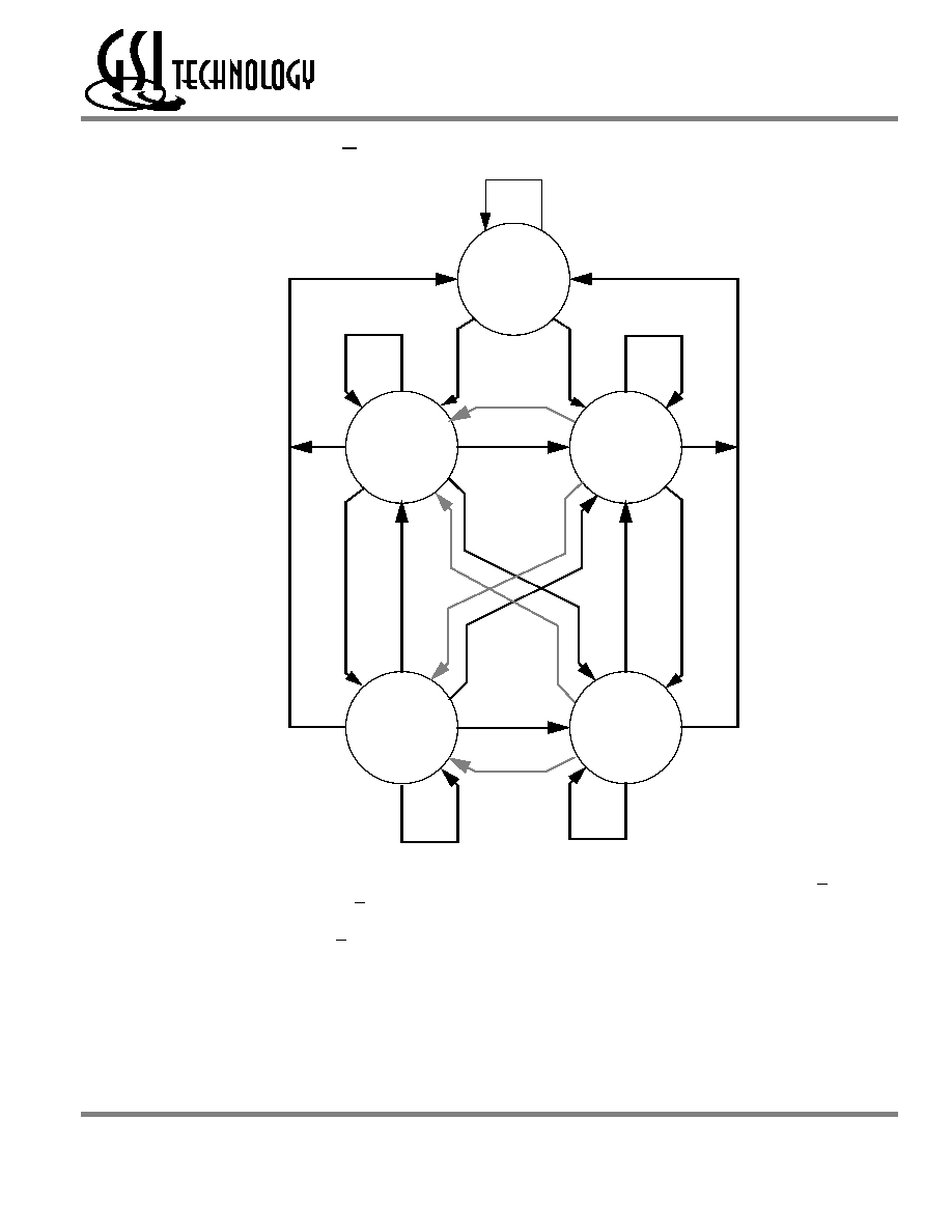
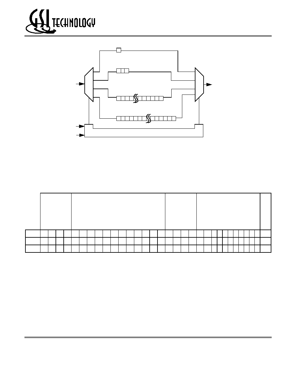
GS88218/36A (PE = 0) Block Diagram
A1
A0
A0
A1
D0
D1
Q1
Q0
Counter
Load
D
Q
D
Q
Register
Register
D
Q
Register
D
Q
Register
D
Q
Register
D
Q
Register
D
Q
Register
D
Q
Register
D
Q
Reg
i
ster
D
Q
Re
giste
r
A0≠An
LBO
ADV
CK
ADSC
ADSP
GW
BW
E
1
FT
G
ZZ
Power Down
Control
Memory
Array
36
36
4
A
Q
D
DQx1≠DQx9
NC
Parity
NC
Parity
Encode
Compare
36
4
36
36
4
32
Note: Only x36 version shown for simplicity.
SCD
36
36
DQ
Regist
er
4
B
A
B
B
B
C
B
D
Rev: 1.03a 9/2002
8/38
© 2001, Giga Semiconductor, Inc.
Specifications cited are subject to change without notice. For latest documentation see http://www.gsitechnology.com.
GS88218/36AB/D-250/225/200/166/150/133
GS88218/36A (PE = 1) x32 Mode Block Diagram
A1
A0
A0
A1
D0
D1
Q1
Q0
Counter
Load
D
Q
D
Q
Register
Register
D
Q
Register
D
Q
Register
D
Q
Register
D
Q
Register
D
Q
Register
D
Q
Register
D
Q
Re
g
i
s
t
e
r
D
Q
Reg
i
s
t
er
A0≠An
LBO
ADV
CK
ADSC
ADSP
GW
BW
B
A
B
B
B
C
B
D
E
1
FT
G
ZZ
Power Down
Control
Memory
Array
36
36
4
A
Q
D
DQx1≠DQx8
NC
Parity
NC
Parity
Encode
Compare
32
4
32
36
4
32
Note: Only x36 version shown for simplicity.
SCD
D
Q
Register
D
Q
Register
Parity
Encode
32
4
32
36
Rev: 1.03a 9/2002
9/38
© 2001, Giga Semiconductor, Inc.
Specifications cited are subject to change without notice. For latest documentation see http://www.gsitechnology.com.
GS88218/36AB/D-250/225/200/166/150/133
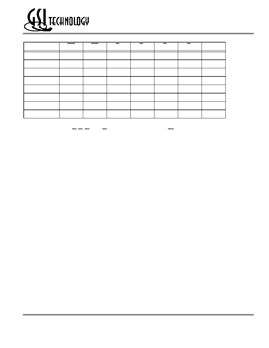
Note:
There are pull-up devices on the SCD and FT pins and a pull-down devices on the ZZ pin, so those input pins can be unconnected and the chip
will operate in the default states as specified in the above tables.
Enable / Disable Parity I/O Pins
This SRAM allows the user to configure the device to operate in Parity I/O active (x18 or x36) or in Parity I/O inactive (x16, x32, or x64) mode.
Holding the PE bump low or letting it float will activate the 9th I/O on each byte of the RAM.
Burst Counter Sequences
BPR 1999.05.18
Mode Pin Functions
Mode Name
Pin
Name
State
Function
Burst Order Control
LBO
L
Linear Burst
H
Interleaved Burst
Output Register Control
FT
L
Flow Through
H or NC
Pipeline
Power Down Control
ZZ
L or NC
Active
H
Standby, I
DD
= I
SB
Single/Dual Cycle Deselect Control
SCD
L
Dual Cycle Deselect
H or NC
Single Cycle Deselect
Linear Burst Sequence
Note: The burst counter wraps to initial state on the 5th clock.
I
nterleaved Burst Sequence
Note: The burst counter wraps to initial state on the 5th clock.
A[1:0] A[1:0] A[1:0] A[1:0]
1st address
00
01
10
11
2nd address
01
10
11
00
3rd address
10
11
00
01
4th address
11
00
01
10
A[1:0] A[1:0] A[1:0] A[1:0]
1st address
00
01
10
11
2nd address
01
00
11
10
3rd address
10
11
00
01
4th address
11
10
01
00
Rev: 1.03a 9/2002
10/38
© 2001, Giga Semiconductor, Inc.
Specifications cited are subject to change without notice. For latest documentation see http://www.gsitechnology.com.
GS88218/36AB/D-250/225/200/166/150/133
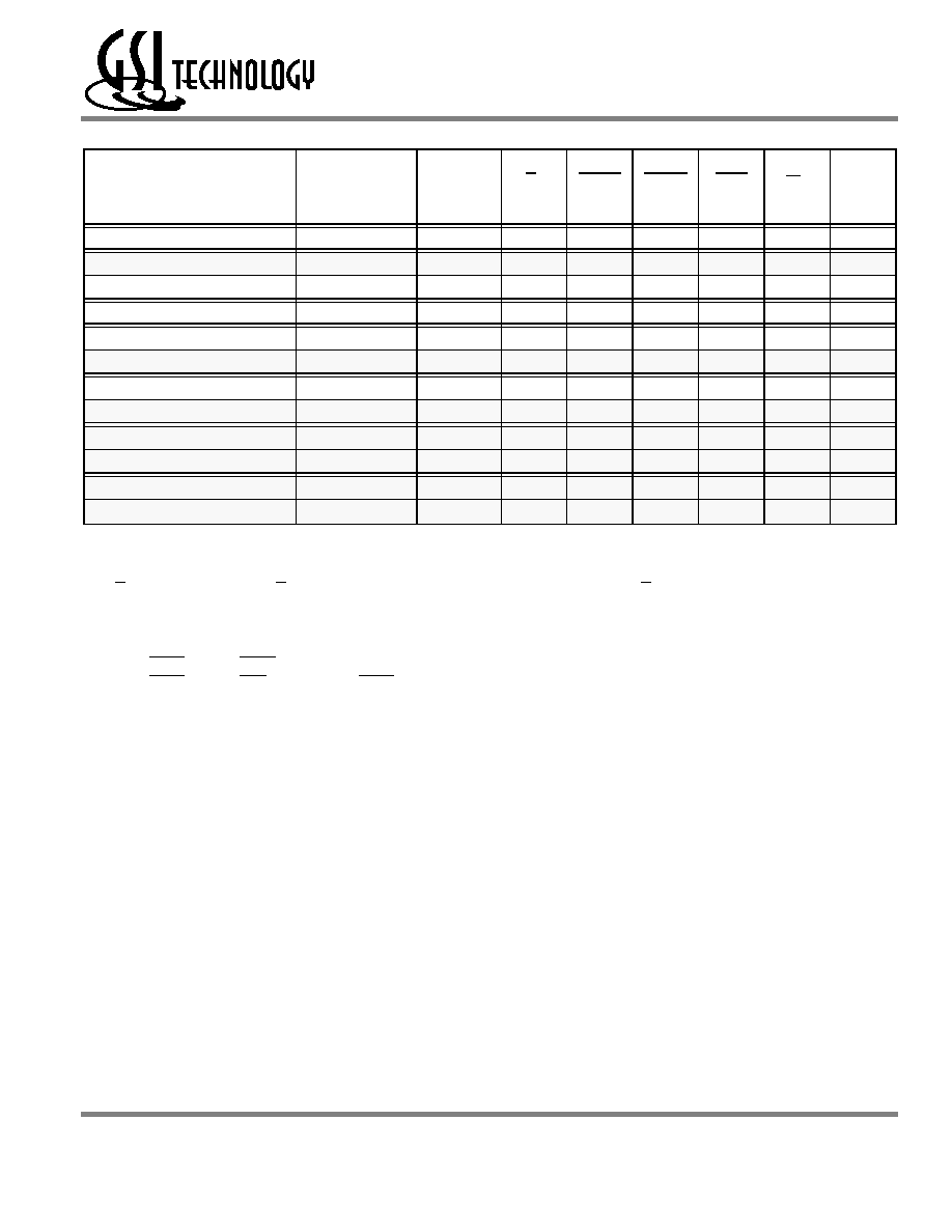
Byte Write Truth Table
Notes:
1. All byte outputs are active in read cycles regardless of the state of Byte Write Enable inputs.
2. Byte Write Enable inputs B
A
, B
B
, B
C
, and/or B
D
may be used in any combination with BW to write single or multiple bytes.
3. All byte I/Os remain High-Z during all write operations regardless of the state of Byte Write Enable inputs.
4. Bytes "
C
" and "
D
" are only available on the x36 version.
Function
GW
BW
B
A
B
B
B
C
B
D
Notes
Read
H
H
X
X
X
X
1
Read
H
L
H
H
H
H
1
Write byte a
H
L
L
H
H
H
2, 3
Write byte b
H
L
H
L
H
H
2, 3
Write byte c
H
L
H
H
L
H
2, 3, 4
Write byte d
H
L
H
H
H
L
2, 3, 4
Write all bytes
H
L
L
L
L
L
2, 3, 4
Write all bytes
L
X
X
X
X
X
Rev: 1.03a 9/2002
11/38
© 2001, Giga Semiconductor, Inc.
Specifications cited are subject to change without notice. For latest documentation see http://www.gsitechnology.com.
GS88218/36AB/D-250/225/200/166/150/133
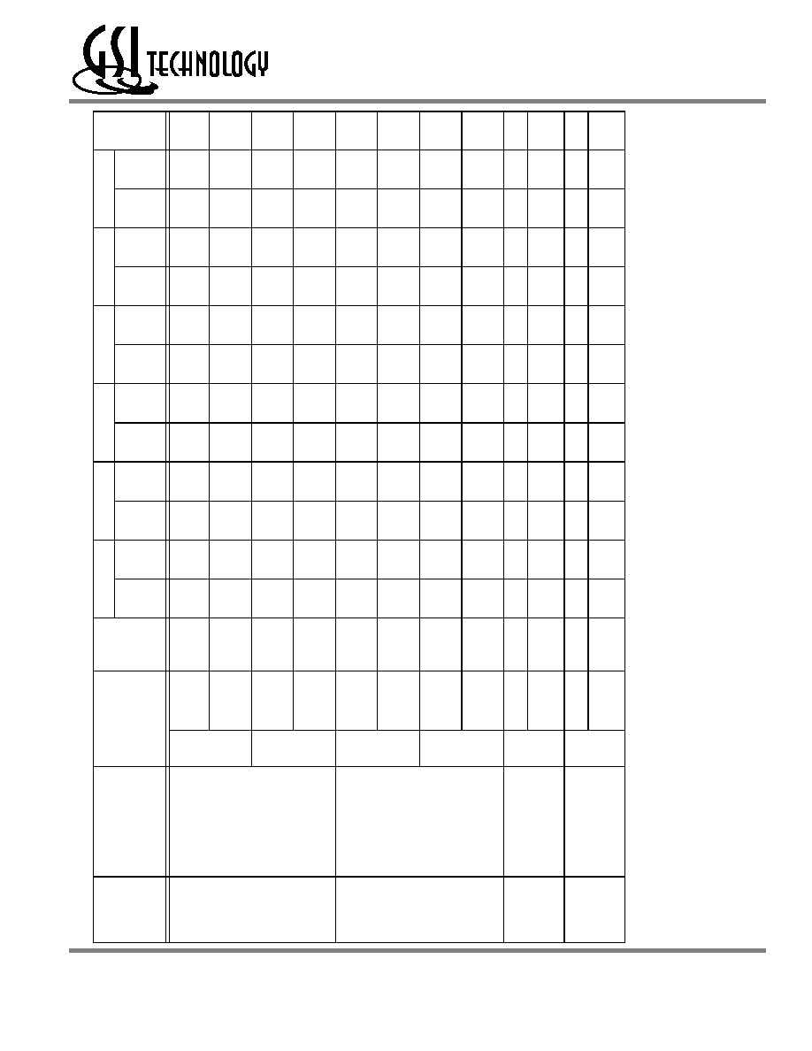
Synchronous Truth Table
Operation
Address Used
State
Diagram
Key
5
E
1
ADSP
ADSC
ADV
W
3
DQ
4
Deselect Cycle, Power Down
None
X
H
X
L
X
X
High-Z
Read Cycle, Begin Burst
External
R
L
L
X
X
X
Q
Read Cycle, Begin Burst
External
R
L
H
L
X
F
Q
Write Cycle, Begin Burst
External
W
L
H
L
X
T
D
Read Cycle, Continue Burst
Next
CR
X
H
H
L
F
Q
Read Cycle, Continue Burst
Next
CR
H
X
H
L
F
Q
Write Cycle, Continue Burst
Next
CW
X
H
H
L
T
D
Write Cycle, Continue Burst
Next
CW
H
X
H
L
T
D
Read Cycle, Suspend Burst
Current
X
H
H
H
F
Q
Read Cycle, Suspend Burst
Current
H
X
H
H
F
Q
Write Cycle, Suspend Burst
Current
X
H
H
H
T
D
Write Cycle, Suspend Burst
Current
H
X
H
H
T
D
Notes:
1. X = Don't Care, H = High, L = Low
2. W = T (True) and F (False) is defined in the Byte Write Truth Table preceding
3. G is an asynchronous input. G can be driven high at any time to disable active output drivers. G low can only enable active drivers (shown
as "Q" in the Truth Table above).
4. All input combinations shown above are tested and supported. Input combinations shown in gray boxes need not be used to accomplish
basic synchronous or synchronous burst operations and may be avoided for simplicity.
5. Tying ADSP high and ADSC low allows simple non-burst synchronous operations. See BOLD items above.
6. Tying ADSP high and ADV low while using ADSC to load new addresses allows simple burst operations. See ITALIC items above.
Rev: 1.03a 9/2002
12/38
© 2001, Giga Semiconductor, Inc.
Specifications cited are subject to change without notice. For latest documentation see http://www.gsitechnology.com.
GS88218/36AB/D-250/225/200/166/150/133
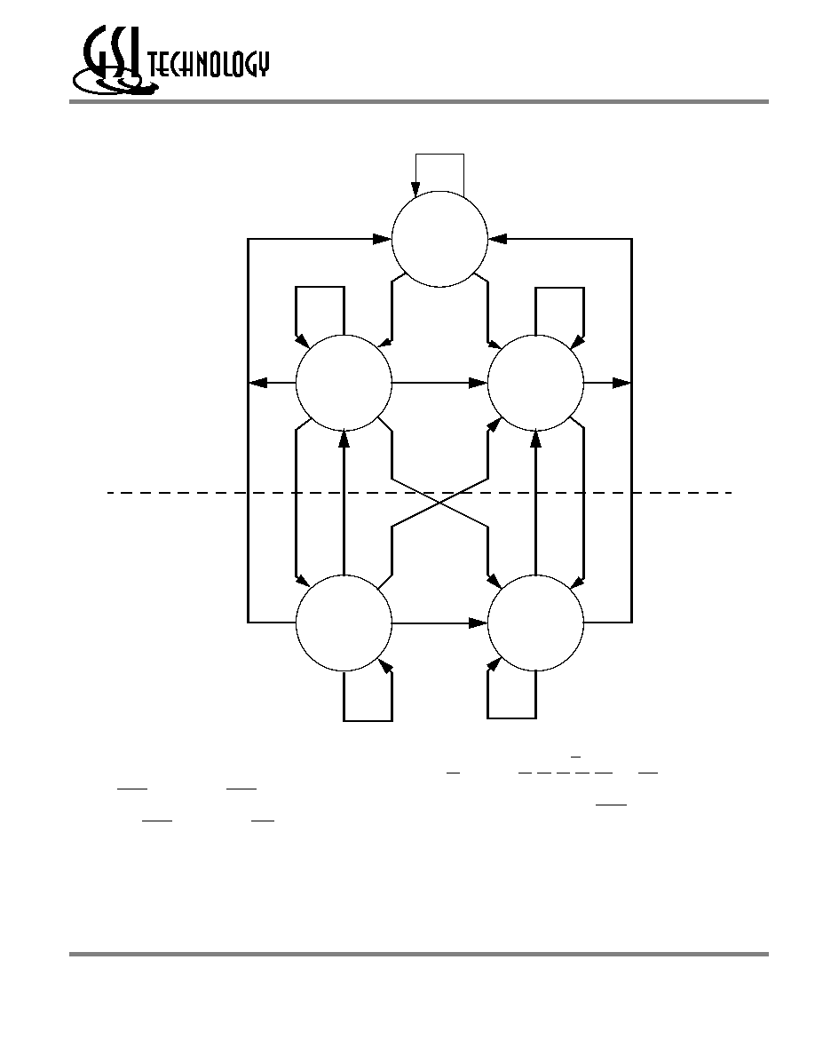
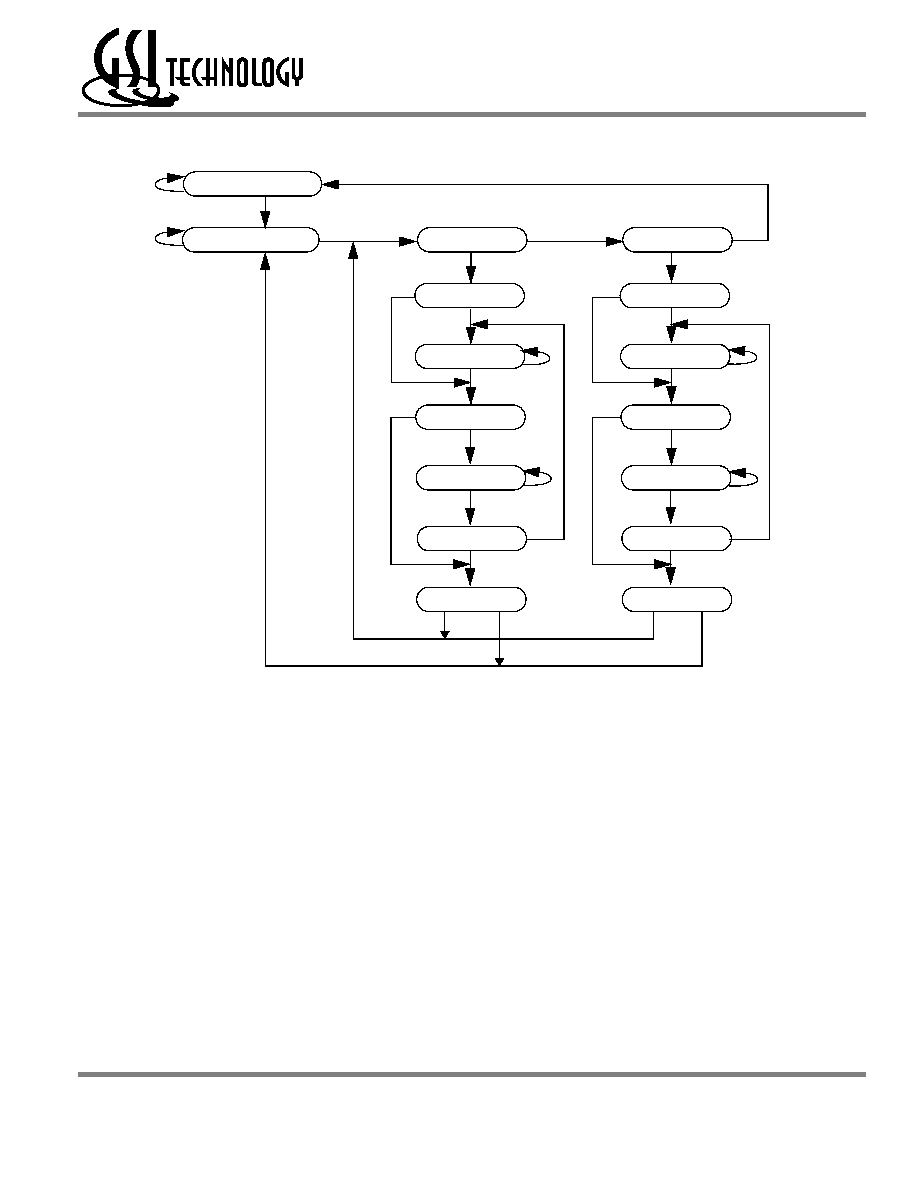
First Write
First Read
Burst Write
Burst Read
Deselect
R
W
CR
CW
X
X
W
R
R
W
R
X
X
X
Simple Synchronous Operation
Simple Burst Synchronou
s Operation
CR
R
CW
CR
CR
Simplified State Diagram
Notes:
1. The diagram shows only supported (tested) synchronous state transitions. The diagram presumes G is tied low.
2. The upper portion of the diagram assumes active use of only the Enable (E1) and Write (B
A
, B
B
, B
C
, B
D
, BW, and GW) control inputs, and
that ADSP is tied high and ADSC is tied low.
3. The upper and lower portions of the diagram together assume active use of only the Enable, Write, and ADSC control inputs and
assumes ADSP is tied high and ADV is tied low.
Rev: 1.03a 9/2002
13/38
© 2001, Giga Semiconductor, Inc.
Specifications cited are subject to change without notice. For latest documentation see http://www.gsitechnology.com.
GS88218/36AB/D-250/225/200/166/150/133
First Write
First Read
Burst Write
Burst Read
Deselect
R
W
CR
CW
X
X
W
R
R
W
R
X
X
X
CR
R
CW
CR
CR
W
CW
W
CW
Simplified State Diagram with G
Notes:
1. The diagram shows supported (tested) synchronous state transitions plus supported transitions that depend upon the use of G.
2. Use of "Dummy Reads" (Read Cycles with G High) may be used to make the transition from read cycles to write cycles without passing
through a Deselect cycle. Dummy Read cycles increment the address counter just like normal read cycles.
3. Transitions shown in grey tone assume G has been pulsed high long enough to turn the RAM's drivers off and for incoming data to meet
Data Input Set Up Time.
Rev: 1.03a 9/2002
14/38
© 2001, Giga Semiconductor, Inc.
Specifications cited are subject to change without notice. For latest documentation see http://www.gsitechnology.com.
GS88218/36AB/D-250/225/200/166/150/133
Note:
Permanent damage to the device may occur if the Absolute Maximum Ratings are exceeded. Operation should be restricted to Recommended
Operating Conditions. Exposure to conditions exceeding the Absolute Maximum Ratings, for an extended period of time, may affect reliability of
this component.
Absolute Maximum Ratings
(All voltages reference to V
SS
)
Symbol
Description
Value
Unit
V
DD
Voltage on V
DD
Pins
≠0.5 to 4.6
V
V
DDQ
Voltage in V
DDQ
Pins
≠0.5 to 4.6
V
V
CK
Voltage on Clock Input Pin
≠0.5 to 6
V
V
I/O
Voltage on I/O Pins
≠0.5 to V
DDQ
+0.5 (
4.6 V max.)
V
V
IN
Voltage on Other Input Pins
≠0.5 to V
DD
+0.5 (
4.6 V max.)
V
I
IN
Input Current on Any Pin
+/≠20
mA
I
OUT
Output Current on Any I/O Pin
+/≠20
mA
P
D
Package Power Dissipation
1.5
W
T
STG
Storage Temperature
≠55 to 125
o
C
T
BIAS
Temperature Under Bias
≠55 to 125
o
C
Rev: 1.03a 9/2002
15/38
© 2001, Giga Semiconductor, Inc.
Specifications cited are subject to change without notice. For latest documentation see http://www.gsitechnology.com.
GS88218/36AB/D-250/225/200/166/150/133
Power Supply Voltage Ranges
Parameter
Symbol
Min.
Typ.
Max.
Unit
Notes
3.3 V Supply Voltage
V
DD3
3.0
3.3
3.6
V
2.5 V Supply Voltage
V
DD2
2.3
2.5
2.7
V
3.3 V V
DDQ
I/O Supply Voltage
V
DDQ3
3.0
3.3
3.6
V
2.5 V V
DDQ
I/O Supply Voltage
V
DDQ2
2.3
2.5
2.7
V
Notes:
1.
The part numbers of Industrial Temperature Range versions end the character "I". Unless otherwise noted, all performance specifications quoted are
evaluated for worst case in the temperature range marked on the device.
2.
Input Under/overshoot voltage must be ≠2 V > Vi < V
DDn
+2 V not to exceed 4.6 V maximum, with a pulse width not to exceed 20% tKC.
V
DDQ3
Range Logic Levels
Parameter
Symbol
Min.
Typ.
Max.
Unit
Notes
V
DD
Input High Voltage
V
IH
2.0
--
V
DD
+ 0.3
V
1
V
DD
Input Low Voltage
V
IL
≠0.3
--
0.8
V
1
V
DDQ
I/O Input High Voltage
V
IHQ
2.0
--
V
DDQ
+ 0.3
V
1,3
V
DDQ
I/O Input Low Voltage
V
ILQ
≠0.3
--
0.8
V
1,3
Notes:
1.
The part numbers of Industrial Temperature Range versions end the character "I". Unless otherwise noted, all performance specifications quoted are
evaluated for worst case in the temperature range marked on the device.
2.
Input Under/overshoot voltage must be ≠2 V > Vi < V
DDn
+2 V not to exceed 4.6 V maximum, with a pulse width not to exceed 20% tKC.
3.
V
IHQ
(max) is voltage on V
DDQ
pins plus 0.3 V.
V
DDQ2
Range Logic Levels
Parameter
Symbol
Min.
Typ.
Max.
Unit
Notes
V
DD
Input High Voltage
V
IH
0.6*V
DD
--
V
DD
+ 0.3
V
1
V
DD
Input Low Voltage
V
IL
≠0.3
--
0.3*V
DD
V
1
V
DDQ
I/O Input High Voltage
V
IHQ
0.6*V
DD
--
V
DDQ
+ 0.3
V
1,3
V
DDQ
I/O Input Low Voltage
V
ILQ
≠0.3
--
0.3*V
DD
V
1,3
Notes:
1.
The part numbers of Industrial Temperature Range versions end the character "I". Unless otherwise noted, all performance specifications quoted are
evaluated for worst case in the temperature range marked on the device.
2.
Input Under/overshoot voltage must be ≠2 V > Vi < V
DDn
+2 V not to exceed 4.6 V maximum, with a pulse width not to exceed 20% tKC.
3.
V
IHQ
(max) is voltage on V
DDQ
pins plus 0.3 V.
Rev: 1.03a 9/2002
16/38
© 2001, Giga Semiconductor, Inc.
Specifications cited are subject to change without notice. For latest documentation see http://www.gsitechnology.com.
GS88218/36AB/D-250/225/200/166/150/133
Note: These parameters are sample tested.
Notes:
1. Junction temperature is a function of SRAM power dissipation, package thermal resistance, mounting board temperature, ambient. Temper-
ature air flow, board density, and PCB thermal resistance.
2. SCMI G-38-87
3. Average thermal resistance between die and top surface, MIL SPEC-883, Method 1012.1
Recommended Operating Temperatures
Parameter
Symbol
Min.
Typ.
Max.
Unit
Notes
Ambient Temperature (Commercial Range Versions)
T
A
0
25
70
∞
C
2
Ambient Temperature (Industrial Range Versions)
T
A
≠40
25
85
∞
C
2
Note:
1.
The part numbers of Industrial Temperature Range versions end the character "I". Unless otherwise noted, all performance specifications quoted are
evaluated for worst case in the temperature range marked on the device.
2.
Input Under/overshoot voltage must be ≠2 V > Vi < V
DDn
+2 V not to exceed 4.6 V maximum, with a pulse width not to exceed 20% tKC.
Capacitance
(T
A
= 25
o
C, f = 1 MH
Z
, V
DD
= 2.5 V)
Parameter
Symbol
Test conditions
Typ.
Max.
Unit
Input Capacitance
C
IN
V
IN
= 0 V
4
5
pF
Input/Output Capacitance
C
I/O
V
OUT
= 0 V
6
7
pF
Package Thermal Characteristics
Rating
Layer Board
Symbol
Max
Unit
Notes
Junction to Ambient (at 200 lfm)
single
R
JA
40
∞
C/W
1,2
Junction to Ambient (at 200 lfm)
four
R
JA
24
∞
C/W
1,2
Junction to Case (TOP)
--
R
JC
9
∞
C/W
3
20% tKC
V
SS
≠ 2.0 V
50%
V
SS
V
IH
Undershoot Measurement and Timing
Overshoot Measurement and Timing
20% tKC
V
DD
+ 2.0 V
50%
V
DD
V
IL

Rev: 1.03a 9/2002
17/38
© 2001, Giga Semiconductor, Inc.
Specifications cited are subject to change without notice. For latest documentation see http://www.gsitechnology.com.
GS88218/36AB/D-250/225/200/166/150/133
AC Test Conditions
Parameter
Conditions
Input high level
V
DD
≠ 0.2 V
Input low level
0.2 V
Input slew rate
1 V/ns
Input reference level
V
DD
/2
Output reference level
V
DDQ
/2
Output load
Fig. 1
Notes:
1. Include scope and jig capacitance.
2. Test conditions as specified with output loading as shown in Fig. 1
unless otherwise noted.
3. Device is deselected as defined by the Truth Table.
DC Electrical Characteristics
Parameter
Symbol
Test Conditions
Min
Max
Input Leakage Current
(except mode pins)
I
IL
V
IN
= 0 to V
DD
≠1 uA
1 uA
ZZ and PE Input Current
I
IN1
V
DD
V
IN
V
IH
0 V
V
IN
V
IH
≠1 uA
≠1 uA
1 uA
100 uA
FT, SCD, ZQ Input Current
I
IN2
V
DD
V
IN
V
IL
0 V
V
IN
V
IL
≠100 uA
≠1 uA
1 uA
1 uA
Output Leakage Current
I
OL
Output Disable, V
OUT
= 0 to V
DD
≠1 uA
1 uA
Output High Voltage
V
OH2
I
OH
= ≠8 mA, V
DDQ
= 2.375 V
1.7 V
--
Output High Voltage
V
OH3
I
OH
= ≠8 mA, V
DDQ
= 3.135 V
2.4 V
--
Output Low Voltage
V
OL
I
OL
= 8 mA
--
0.4 V
DQ
V
DDQ/2
50
30pF
*
Output Load 1
* Distributed Test Jig Capacitance
Rev: 1.03a 9/2002
18/38
© 2001, Giga Semiconductor, Inc.
Specifications cited are subject to change without notice. For latest documentation see http://www.gsitechnology.com.
GS88218/36AB/D-250/225/200/166/150/133
Operatin
g Curren
ts
Notes:
1.
I
DD
and I
DDQ
apply to any combination of V
DD3
, V
DD2
, V
DDQ3
, and
V
DD
Q
2
operation.
2.
All parameters listed are worst case scenario.
Parameter
T
est Conditions
Mode
Symbol
-250
-225
-200
-166
-150
-133
Un
it
0
to
70∞C
≠
40
to
85∞C
0
to
70∞C
≠
40
to
85∞C
0
to
70
∞
C
≠
40
to
85∞C
0
to
70∞C
≠
40
to
85∞C
0
to
70∞C
≠
40
to
85∞C
0
to
70∞C
≠
40
to
85∞C
Operating
Current
3.3 V
D
e
vic
e
S
e
lected;
All other inputs
V
IH
o
r
V
IL
Out
p
ut
ope
n
(x36)
Pi
peline
I
DD
I
DDQ
290
40
300
40
265
35
275
35
240
30
250
30
205
25
215
25
190
25
200
25
170
20
180
20
mA
Fl
ow
Through
I
DD
I
DDQ
180
20
190
20
170
20
180
20
165
15
175
15
155
15
165
15
150
15
160
15
140
10
150
10
mA
(x18)
Pi
peline
I
DD
I
DDQ
260
20
270
20
235
20
245
20
215
15
225
15
185
15
195
15
170
15
180
15
155
10
165
10
mA
Fl
ow
Through
I
DD
I
DDQ
165
10
175
10
155
10
165
10
150
10
160
10
140
10
150
10
135
10
145
10
125
10
135
10
mA
Operating
Current
2.5 V
D
e
vic
e
S
e
lected;
All other inputs
V
IH
o
r
V
IL
Out
p
ut
ope
n
(x36)
Pi
peline
I
DD
I
DDQ
290
30
300
30
265
30
275
30
240
25
250
25
205
20
215
20
190
20
200
20
170
15
180
15
mA
Fl
ow
Through
I
DD
I
DDQ
180
20
190
20
170
20
180
20
165
15
175
15
155
15
165
15
150
15
160
15
140
10
150
10
mA
(x18)
Pi
peline
I
DD
I
DDQ
260
15
270
15
235
15
245
15
215
15
225
15
185
10
195
10
170
10
180
10
155
10
165
10
mA
Fl
ow
Through
I
DD
I
DDQ
165
10
175
10
155
10
165
10
150
10
160
10
140
10
150
10
135
10
145
10
125
10
135
10
mA
Standby
Current
ZZ
V
DD
≠
0.
2
V
--
Pi
peline
I
SB
20
30
20
30
20
30
20
30
20
30
20
30
mA
Fl
ow
Through
I
SB
20
30
20
30
20
30
20
30
20
30
20
30
mA
Des
e
l
e
ct
Current
D
e
vic
e
Desel
e
cted;
All other inputs
V
IH
or
V
IL
--
Pi
peline
I
DD
85
90
80
85
75
80
64
70
60
65
50
55
mA
Fl
ow
Through
I
DD
60
65
60
65
50
55
50
55
50
55
45
50
mA

Rev: 1.03a 9/2002
19/38
© 2001, Giga Semiconductor, Inc.
Specifications cited are subject to change without notice. For latest documentation see http://www.gsitechnology.com.
GS88218/36AB/D-250/225/200/166/150/133
AC Electrical Characteristics
Notes:
1. These parameters are sampled and are not 100% tested.
2. ZZ is an asynchronous signal. However, in order to be recognized on any given clock cycle, ZZ must meet the specified setup and hold
times as specified above.
Parameter
Symbol
-250
-225
-200
-166
-150
-133
Unit
Min
Max
Min
Max
Min
Max
Min
Max Min Max Min Max
Pipeline
Clock Cycle Time
tKC
4.0
--
4.4
--
5.0
--
6.0
--
6.7
--
7.5
--
ns
Clock to Output Valid
tKQ
--
2.5
--
2.7
--
3.0
--
3.4
--
3.8
--
4.0
ns
Clock to Output Invalid
tKQX
1.5
--
1.5
--
1.5
--
1.5
--
1.5
--
1.5
--
ns
Clock to Output in Low-Z
tLZ
1
1.5
--
1.5
--
1.5
--
1.5
--
1.5
--
1.5
--
ns
Setup time
tS
1.2
--
1.3
--
1.4
--
1.5
--
1.5
--
1.5
--
ns
Hold time
tH
0.2
--
0.3
--
0.4
--
0.5
--
0.5
--
0.5
--
ns
Flow
Through
Clock Cycle Time
tKC
5.5
--
6.0
--
6.5
--
7.0
--
7.5
--
8.5
--
ns
Clock to Output Valid
tKQ
--
5.5
--
6.0
--
6.5
--
7.0
--
7.5
--
8.5
ns
Clock to Output Invalid
tKQX
3.0
--
3.0
--
3.0
--
3.0
--
3.0
--
3.0
--
ns
Clock to Output in Low-Z
tLZ
1
3.0
--
3.0
--
3.0
--
3.0
--
3.0
--
3.0
--
ns
Setup time
tS
1.5
--
1.5
--
1.5
--
1.5
--
1.5
--
1.5
--
ns
Hold time
tH
0.5
--
0.5
--
0.5
--
0.5
--
0.5
--
0.5
--
ns
Clock HIGH Time
tKH
1.3
--
1.3
--
1.3
--
1.3
--
1.5
--
1.7
--
ns
Clock LOW Time
tKL
1.5
--
1.5
--
1.5
--
1.5
--
1.7
--
2
--
ns
Clock to Output in
High-Z
tHZ
1
1.5 2.3
1.5 2.5
1.5 3.0
1.5
3.0
1.5 3.0
1.5 3.0
ns
G to Output Valid
tOE
--
2.3
--
2.5
--
3.2
--
3.5
--
3.8
--
4.0
ns
G to output in Low-Z
tOLZ
1
0
--
0
--
0
--
0
--
0
--
0
--
ns
G to output in High-Z
tOHZ
1
--
2.3
--
2.5
--
3.0
--
3.0
--
3.0
--
3.0
ns
ZZ setup time
tZZS
2
5
--
5
--
5
--
5
--
5
--
5
--
ns
ZZ hold time
tZZH
2
1
--
1
--
1
--
1
--
1
--
1
--
ns
ZZ recovery
tZZR
20
--
20
--
20
--
20
--
20
--
20
--
ns
Rev: 1.03a 9/2002
20/38
© 2001, Giga Semiconductor, Inc.
Specifications cited are subject to change without notice. For latest documentation see http://www.gsitechnology.com.
GS88218/36AB/D-250/225/200/166/150/133
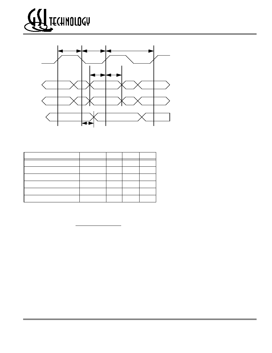
CK
ADSP
ADSC
ADV
GW
BW
WR2
WR3
WR1
WR1
WR2
WR3
tKC
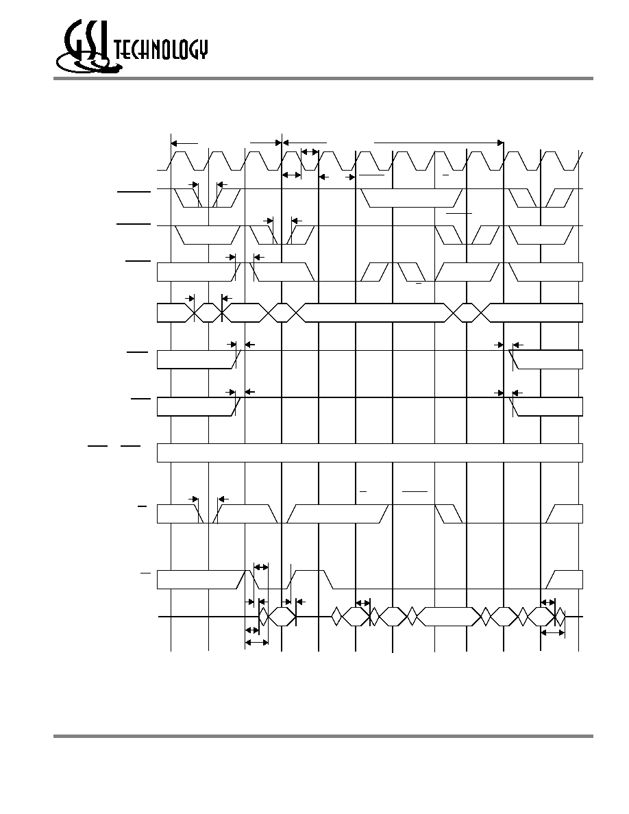
Single Write
Burst Write
t
KL
t
KH
tS tH
tS tH
tS tH
tS tH
tS tH
tS
tH
tS tH
Write specified byte for 2
A
and all bytes for 2
B
, 2
C
& 2
D
ADV must be inactive for ADSP Write
ADSC initiated write
ADSP is blocked by E inactive
A
0
≠An
B
A
≠B
D
DQ
A
≠DQ
D
Write
Deselected
WR1
WR2
WR3
Write Cycle Timing
E
1
tS tH
E
1
only sampled with ADSP or ADSC
E
1
masks ADSP
G
D2
A
D2
B
D2
C
D2
D
D3
A
D1
A
Hi-Z
tS tH
Rev: 1.03a 9/2002
21/38
© 2001, Giga Semiconductor, Inc.
Specifications cited are subject to change without notice. For latest documentation see http://www.gsitechnology.com.
GS88218/36AB/D-250/225/200/166/150/133
Q1
A
Q3
A
Q2
D
Q2c
Q2
B
Q2
A
tKQ
tLZ
tOE
tOHZ
tOLZ
tKQX
tHZ
tKQX
CK
ADSP
ADSC
BW
G
GW
ADV
Burst Read
RD2
RD3
tKL
tS
tH
tH
tS tH
tS tH
ADSC initiated read
Suspend Burst
Single Read
ADSP is blocked by E inactive
A
0
≠An
B
A
≠B
D
tKH
tKC
tS tH
tS
tS
tH
DQ
A
≠DQ
D
RD1
Hi-Z
Suspend Burst
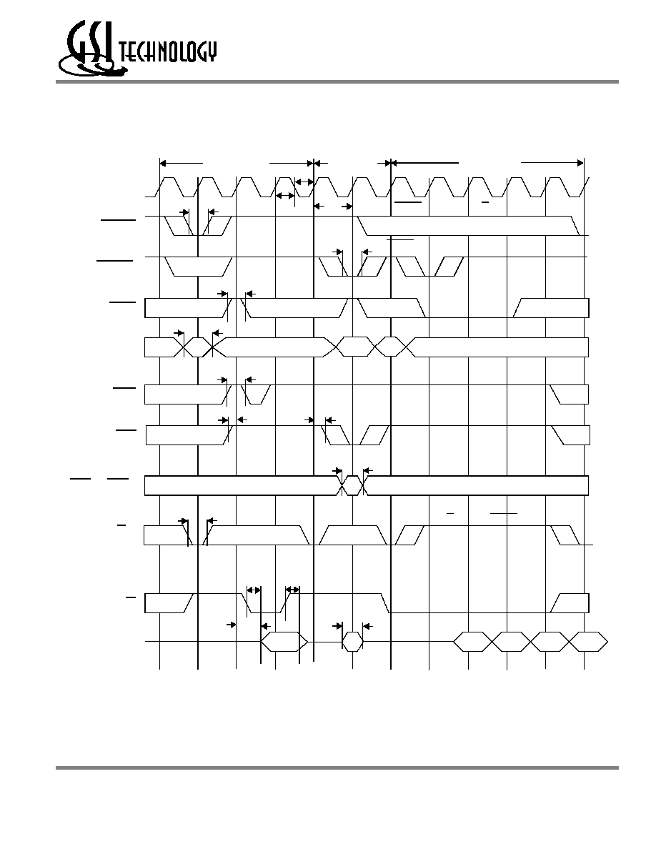
Flow Through Read Cycle Timing
tH
E
1
masks ADSP
E
1
tS
Rev: 1.03a 9/2002
22/38
© 2001, Giga Semiconductor, Inc.
Specifications cited are subject to change without notice. For latest documentation see http://www.gsitechnology.com.
GS88218/36AB/D-250/225/200/166/150/133
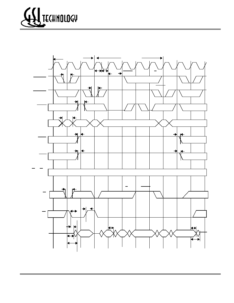
Flow Through Read-Write Cycle Timing
CK
ADSP
ADV
GW
BW
G
Q1
A
D1
A
Q2
A
Q2
B
Q2c
Q2
D
Single Read
Burst Read
tOE
tOHZ
tS tH
tS
tH
tH
tS tH
tS tH
tKH
DQ
A
≠DQ
D
B
A
≠B
D
tKL
tKC
tS
Single Write
ADSP is blocked by E inactive
tKQ
tS
tH
Hi-Z
Q2
A
Burst wrap around to it's initial state
WR1
E
1
tS
E
1
masks ADSP
tH
RD1
WR1
RD2
tS tH
A
0
≠An
ADSC
tS tH
ADSC initiated read
Rev: 1.03a 9/2002
23/38
© 2001, Giga Semiconductor, Inc.
Specifications cited are subject to change without notice. For latest documentation see http://www.gsitechnology.com.
GS88218/36AB/D-250/225/200/166/150/133
Pipelined SCD Read Cycle Timing
Q1
A
Q3
A
Q2
D
Q2c
Q2
B
Q2
A
tKQ
tLZ
tOE
tOHZ
tOLZ
tKQX
tHZ
tKQX
CK
ADSP
ADSC
BW
G
GW
ADV
Burst Read
RD2
RD3
tKL
tS
tH
tH
tS tH
tS tH
ADSC initiated read
Suspend Burst
Single Read
ADSP is blocked by E inactive
A
0
≠An
BW
A
≠BW
D
tKH
tKC
tS tH
tS
tS
tH
DQ
A
≠DQ
D
RD1
Hi-Z
tH
E
1
masks ADSP
E
1
tS
Rev: 1.03a 9/2002
24/38
© 2001, Giga Semiconductor, Inc.
Specifications cited are subject to change without notice. For latest documentation see http://www.gsitechnology.com.
GS88218/36AB/D-250/225/200/166/150/133
CK
ADSP
ADV
GW
BW
G
Q1
A
D1
A
Q2
A
Q2
B
Q2c
Q2
D
Single Read
Burst Read
tOE
tOHZ
tS tH
tS
tH
tH
tS tH
tS tH
tKH
DQ
A
≠DQ
D
BW
A
≠ BW
D
tKL
tKC
tS
Single Write
ADSP is blocked by E inactive
tKQ
tS tH
Hi-Z
Pipelined SCD Read-Write Cycle Timing
WR1
E
1
tS
E
1
masks ADSP
tH
RD1
WR1
RD2
tS tH
A
0
≠An
ADSC
tS tH
ADSC initiated read

Rev: 1.03a 9/2002
25/38
© 2001, Giga Semiconductor, Inc.
Specifications cited are subject to change without notice. For latest documentation see http://www.gsitechnology.com.
GS88218/36AB/D-250/225/200/166/150/133
Pipelined DCD Read Cycle Timing
Q1
A
Q3
A
Q2
D
Q2c
Q2
B
Q2
A
tKQ
tLZ
tOE
tOHZ
tOLZ
tKQX
tHZ
tKQX
CK
ADSP
BW
G
GW
ADV
Burst Read
RD2
RD3
tKL
tH
tS
tH
tH
tS tH
tS tH
Suspend Burst
E
1
masks ADSP
Single Read
ADSP is blocked by E1 inactive
A
0
≠An
B
A
≠B
D
E
1
tKH
tKC
tS
tS
tH
DQ
A
≠DQ
D
tS
RD1
Hi-Z
ADSC
tS tH
ADSC initiated read

Rev: 1.03a 9/2002
26/38
© 2001, Giga Semiconductor, Inc.
Specifications cited are subject to change without notice. For latest documentation see http://www.gsitechnology.com.
GS88218/36AB/D-250/225/200/166/150/133
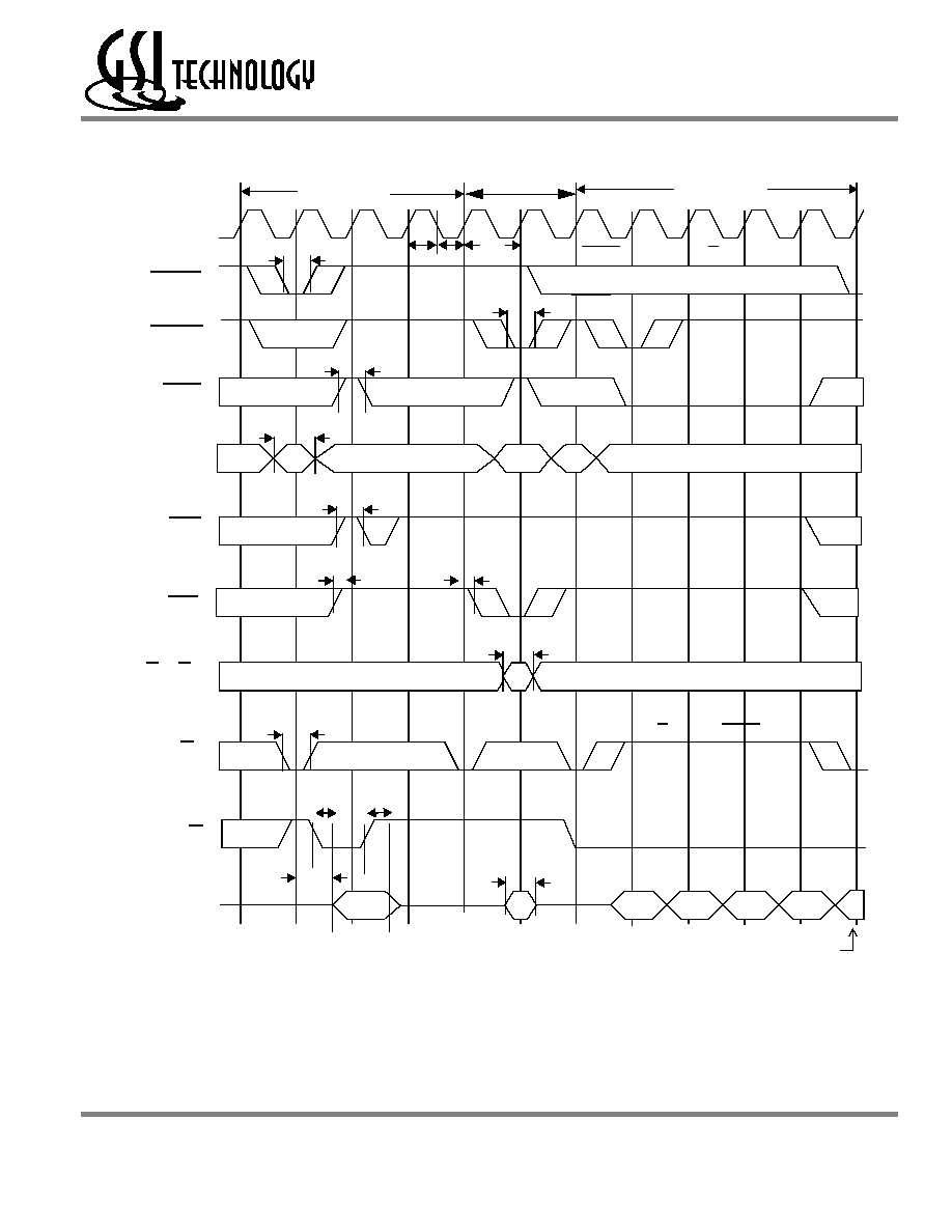
Pipelined DCD Read-Write Cycle Timing
CK
ADSP
ADSC
ADV
GW
BW
E
1
G
WR1
Q1
A
D1
A
Q2
A
Q2
B
Q2c
Q2
D
Single Read
Burst Read
tOE
tOHZ
tS
tS tH
tS
tH
tH
tS tH
tS tH
tS tH
tKH
ADSC initiated read
E
1
masks ADSP
DQ
A
≠DQ
D
tKL
tKC
tS
tH
Single Write
ADSP is blocked by E1 inactive
tKQ
tS tH
Hi-Z
B
A
≠B
D
RD1
RD2
tS tH
A
0
≠An
WR1
Rev: 1.03a 9/2002
27/38
© 2001, Giga Semiconductor, Inc.
Specifications cited are subject to change without notice. For latest documentation see http://www.gsitechnology.com.
GS88218/36AB/D-250/225/200/166/150/133
Sleep Mode
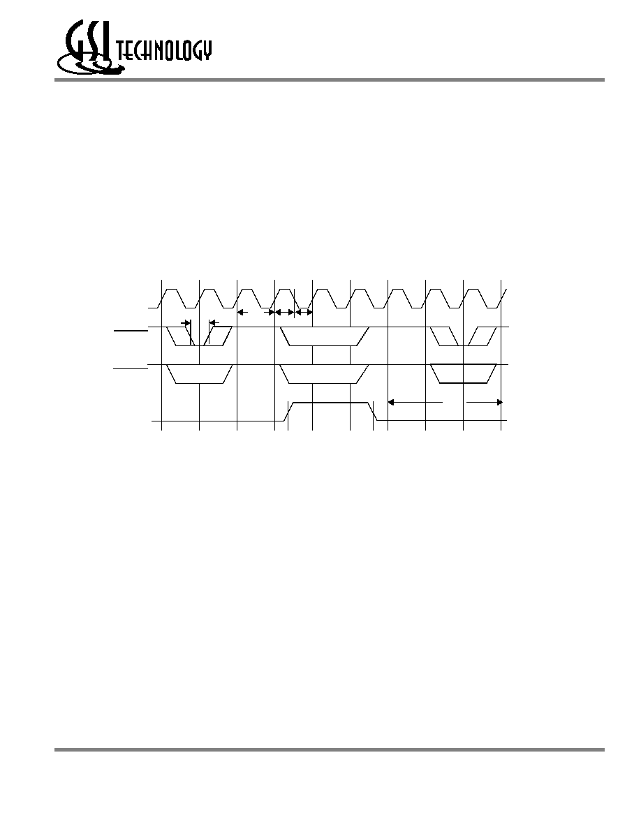
During normal operation, ZZ must be pulled low, either by the user or by it's internal pull down resistor. When ZZ is pulled high,
the SRAM will enter a Power Sleep mode after 2 cycles. At this time, internal state of the SRAM is preserved. When ZZ returns to
low, the SRAM operates normally after ZZ recovery time.
Sleep mode is a low current, power-down mode in which the device is deselected and current is reduced to I
SB
2. The duration of
Sleep mode is dictated by the length of time the ZZ is in a high state. After entering Sleep mode, all inputs except ZZ become
disabled and all outputs go to High-Z The ZZ pin is an asynchronous, active high input that causes the device to enter Sleep mode.
When the ZZ pin is driven high, I
SB
2 is guaranteed after the time tZZI is met. Because ZZ is an asynchronous input, pending
operations or operations in progress may not be properly completed if ZZ is asserted. Therefore, Sleep mode must not be initiated
until valid pending operations are completed. Similarly, when exiting Sleep mode during tZZR, only a Deselect or Read commands
may be applied while the SRAM is recovering from Sleep mode.
Application Tips
Single and Dual Cycle Deselect
SCD devices (like this one) force the use of "dummy read cycles" (read cycles that are launched normally, but that are ended with
the output drivers inactive) in a fully synchronous environment. Dummy read cycles waste performance, but their use usually
assures there will be no bus contention in transitions from reads to writes or between banks of RAMs. DCD SRAMs do not waste
bandwidth on dummy cycles and are logically simpler to manage in a multiple bank application (wait states need not be inserted at
bank address boundary crossings), but greater care must be exercised to avoid excessive bus contention.
JTAG Port Operation
Overview
The JTAG Port on this RAM operates in a manner that is compliant with IEEE Standard 1149.1-1990, a serial boundary scan
interface standard (commonly referred to as JTAG). The JTAG Port input interface levels scale with V
DD
. The JTAG output
drivers are powered by V
DDQ
.
Disabling the JTAG Port
It is possible to use this device without utilizing the JTAG port. The port is reset at power-up and will remain inactive unless
clocked. TCK, TDI, and TMS are designed with internal pull-up circuits.To assure normal operation of the RAM with the JTAG
Port unused, TCK, TDI, and TMS may be left floating or tied to either V
DD
or V
SS
. TDO should be left unconnected.
CK
ADSP
ADSC
tH
tKH tKL
tKC
tS
ZZ
tZZR
tZZH
tZZS
~ ~
~ ~
~ ~
~ ~
~ ~
~ ~
Snooze
Sleep Mode Timing Diagram
~ ~
~ ~
~ ~
~ ~
~ ~
Rev: 1.03a 9/2002
28/38
© 2001, Giga Semiconductor, Inc.
Specifications cited are subject to change without notice. For latest documentation see http://www.gsitechnology.com.
GS88218/36AB/D-250/225/200/166/150/133
JTAG Port Registers
Overview
The various JTAG registers, refered to as Test Access Port orTAP Registers, are selected (one at a time) via the sequences of 1s and
0s applied to TMS as TCK is strobed. Each of the TAP Registers is a serial shift register that captures serial input data on the rising
edge of TCK and pushes serial data out on the next falling edge of TCK. When a register is selected, it is placed between the TDI
and TDO pins.
Instruction Register
The Instruction Register holds the instructions that are executed by the TAP controller when it is moved into the Run, Test/Idle, or
the various data register states. Instructions are 3 bits long. The Instruction Register can be loaded when it is placed between the
TDI and TDO pins. The Instruction Register is automatically preloaded with the IDCODE instruction at power-up or whenever the
controller is placed in Test-Logic-Reset state.
Bypass Register
The Bypass Register is a single bit register that can be placed between TDI and TDO. It allows serial test data to be passed through
the RAM's JTAG Port to another device in the scan chain with as little delay as possible.
Boundary Scan Register
The Boundary Scan Register is a collection of flip flops that can be preset by the logic level found on the RAM's input or I/O pins.
The flip flops are then daisy chained together so the levels found can be shifted serially out of the JTAG Port's TDO pin. The
Boundary Scan Register also includes a number of place holder flip flops (always set to a logic 1). The relationship between the
device pins and the bits in the Boundary Scan Register is described in the Scan Order Table following. The Boundary Scan
Register, under the control of the TAP Controller, is loaded with the contents of the RAMs I/O ring when the controller is in
Capture-DR state and then is placed between the TDI and TDO pins when the controller is moved to Shift-DR state. SAMPLE-Z,
SAMPLE/PRELOAD and EXTEST instructions can be used to activate the Boundary Scan Register.
JTAG Pin Descriptions
Pin
Pin Name
I/O
Description
TCK
Test Clock
In
Clocks all TAP events. All inputs are captured on the rising edge of TCK and all outputs propagate
from the falling edge of TCK.
TMS
Test Mode Select
In
The TMS input is sampled on the rising edge of TCK. This is the command input for the TAP
controller state machine. An undriven TMS input will produce the same result as a logic one input
level.
TDI
Test Data In
In
The TDI input is sampled on the rising edge of TCK. This is the input side of the serial registers
placed between TDI and TDO. The register placed between TDI and TDO is determined by the
state of the TAP Controller state machine and the instruction that is currently loaded in the TAP
Instruction Register (refer to the TAP Controller State Diagram). An undriven TDI pin will produce
the same result as a logic one input level.
TDO
Test Data Out
Out
Output that is active depending on the state of the TAP state machine. Output changes in
response to the falling edge of TCK. This is the output side of the serial registers placed between
TDI and TDO.
Note:
This device does not have a TRST (TAP Reset) pin. TRST is optional in IEEE 1149.1. The Test-Logic-Reset state is entered while TMS is
held high for five rising edges of TCK. The TAP Controller is also reset automaticly at power-up.
Rev: 1.03a 9/2002
29/38
© 2001, Giga Semiconductor, Inc.
Specifications cited are subject to change without notice. For latest documentation see http://www.gsitechnology.com.
GS88218/36AB/D-250/225/200/166/150/133
JTAG TAP Block Diagram
Identification (ID) Register
The ID Register is a 32-bit register that is loaded with a device and vendor specific 32-bit code when the controller is put in
Capture-DR state with the IDCODE command loaded in the Instruction Register. The code is loaded from a 32-bit on-chip ROM.
It describes various attributes of the RAM as indicated below. The register is then placed between the TDI and TDO pins when the
controller is moved into Shift-DR state. Bit 0 in the register is the LSB and the first to reach TDO when shifting begins.
Tap Controller Instruction Set
Overview
There are two classes of instructions defined in the Standard 1149.1-1990; the standard (Public) instructions, and device specific
(Private) instructions. Some Public instructions are mandatory for 1149.1 compliance. Optional Public instructions must be
implemented in prescribed ways. The TAP on this device may be used to monitor all input and I/O pads, and can be used to load
address, data or control signals into the RAM or to preload the I/O buffers.
When the TAP controller is placed in Capture-IR state the two least significant bits of the instruction register are loaded with 01.
When the controller is moved to the Shift-IR state the Instruction Register is placed between TDI and TDO. In this state the desired
instruction is serially loaded through the TDI input (while the previous contents are shifted out at TDO). For all instructions, the
TAP executes newly loaded instructions only when the controller is moved to Update-IR state. The TAP instruction set for this
device is listed in the following table.
ID Register Contents
Die
Revision
Code
Not Used
I/O
Configuration
GSI Technology
JEDEC Vendor
ID Code
Presence Register
Bit # 31 30 29 28 27 26 25 24 23 22 21 20 19 18 17 16 15 14 13 12 11 10 9 8 7 6 5 4 3 2 1
0
x36
1
X X X
0
0
0
0
0
0
0
0
0
0
0
0
1
0
0
0
0
0 0 1 1 0 1 1 0 0 1
1
x18
1
X X X
0
0
0
0
0
0
0
0
0
0
0
0
1
0
1
0
0
0 0 1 1 0 1 1 0 0 1
1
Instruction Register
ID Code Register
Boundary Scan Register
0
1
2
0
1
2
∑
∑ ∑ ∑
31 30 29
0
1
2
∑ ∑ ∑
∑ ∑ ∑
∑ ∑ ∑
n
0
Bypass Register
TDI
TDO
TMS
TCK
Test Access Port (TAP) Controller
Rev: 1.03a 9/2002
30/38
© 2001, Giga Semiconductor, Inc.
Specifications cited are subject to change without notice. For latest documentation see http://www.gsitechnology.com.
GS88218/36AB/D-250/225/200/166/150/133
JTAG Tap Controller State Diagram
Instruction Descriptions
BYPASS
When the BYPASS instruction is loaded in the Instruction Register the Bypass Register is placed between TDI and TDO. This occurs when
the TAP controller is moved to the Shift-DR state. This allows the board level scan path to be shortened to facilitate testing of other devices
in the scan path.
SAMPLE/PRELOAD
SAMPLE/PRELOAD is a Standard 1149.1 mandatory public instruction. When the SAMPLE / PRELOAD instruction is loaded in the Instruc-
tion Register, moving the TAP controller into the Capture-DR state loads the data in the RAMs input and I/O buffers into the Boundary Scan
Register. Boundary Scan Register locations are not associated with an input or I/O pin, and are loaded with the default state identified in the
Boundary Scan Chain table at the end of this section of the datasheet. Because the RAM clock is independent from the TAP Clock (TCK) it
is possible for the TAP to attempt to capture the I/O ring contents while the input buffers are in transition (i.e. in a metastable state). Although
allowing the TAP to sample metastable inputs will not harm the device, repeatable results cannot be expected. RAM input signals must be
stabilized for long enough to meet the TAPs input data capture set-up plus hold time (tTS plus tTH). The RAMs clock inputs need not be
paused for any other TAP operation except capturing the I/O ring contents into the Boundary Scan Register. Moving the controller to Shift-
DR state then places the boundary scan register between the TDI and TDO pins.
EXTEST
Select DR
Capture DR
Shift DR
Exit1 DR
Pause DR
Exit2 DR
Update DR
Select IR
Capture IR
Shift IR
Exit1 IR
Pause IR
Exit2 IR
Update IR
Test Logic Reset
Run Test Idle
0
0
1
0
1
1
0
0
1
1
1
0
0
1
1
0
0
0
0
1
1
0
0
1
1
0
0
0
1
1
1
1

Rev: 1.03a 9/2002
31/38
© 2001, Giga Semiconductor, Inc.
Specifications cited are subject to change without notice. For latest documentation see http://www.gsitechnology.com.
GS88218/36AB/D-250/225/200/166/150/133
EXTEST is an IEEE 1149.1 mandatory public instruction. It is to be executed whenever the instruction register is loaded with all logic 0s. The
EXTEST command does not block or override the RAM's input pins; therefore, the RAM's internal state is still determined by its input pins.
Typically, the Boundary Scan Register is loaded with the desired pattern of data with the SAMPLE/PRELOAD command. Then the EXTEST
command is used to output the Boundary Scan Register's contents, in parallel, on the RAM's data output drivers on the falling edge of TCK
when the controller is in the Update-IR state.
Alternately, the Boundary Scan Register may be loaded in parallel using the EXTEST command. When the EXTEST instruction is selected,
the sate of all the RAM's input and I/O pins, as well as the default values at Scan Register locations not associated with a pin, are trans-
ferred in parallel into the Boundary Scan Register on the rising edge of TCK in the Capture-DR state, the RAM's output pins drive out the
value of the Boundary Scan Register location with which each output pin is associated.
IDCODE
The IDCODE instruction causes the ID ROM to be loaded into the ID register when the controller is in Capture-DR mode and places the ID
register between the TDI and TDO pins in Shift-DR mode. The IDCODE instruction is the default instruction loaded in at power up and any
time the controller is placed in the Test-Logic-Reset state.
SAMPLE-Z
If the SAMPLE-Z instruction is loaded in the instruction register, all RAM outputs are forced to an inactive drive state (high-Z) and the Bound-
ary Scan Register is connected between TDI and TDO when the TAP controller is moved to the Shift-DR state.
RFU
These instructions are Reserved for Future Use. In this device they replicate the BYPASS instruction.
JTAG TAP Instruction Set Summary
Instruction
Code
Description
Notes
EXTEST
000
Places the Boundary Scan Register between TDI and TDO.
1
IDCODE
001
Preloads ID Register and places it between TDI and TDO.
1, 2
SAMPLE-Z
010
Captures I/O ring contents. Places the Boundary Scan Register between TDI and TDO.
Forces all RAM output drivers to High-Z.
1
RFU
011
Do not use this instruction; Reserved for Future Use.
Replicates BYPASS instruction. Places Bypass Register between TDI and TDO.
1
SAMPLE/PRELOAD
100
Captures I/O ring contents. Places the Boundary Scan Register between TDI and TDO.
1
GSI
101
GSI private instruction.
1
RFU
110
Do not use this instruction; Reserved for Future Use.
Replicates BYPASS instruction. Places Bypass Register between TDI and TDO.
1
BYPASS
111
Places Bypass Register between TDI and TDO.
1
Notes:
1. Instruction codes expressed in binary, MSB on left, LSB on right.
2. Default instruction automatically loaded at power-up and in test-logic-reset state.
Rev: 1.03a 9/2002
32/38
© 2001, Giga Semiconductor, Inc.
Specifications cited are subject to change without notice. For latest documentation see http://www.gsitechnology.com.
GS88218/36AB/D-250/225/200/166/150/133
JTAG Port Recommended Operating Conditions and DC Characteristics
Parameter
Symbol
Min.
Max.
Unit Notes
3.3 V Test Port Input High Voltage
V
IHJ3
2.0
V
DD3
+0.3
V
1
3.3 V Test Port Input Low Voltage
V
ILJ3
≠0.3
0.8
V
1
2.5 V Test Port Input High Voltage
V
IHJ2
0.6 * V
DD2
V
DD2
+0.3
V
1
2.5 V Test Port Input Low Voltage
V
ILJ2
≠0.3
0.3 * V
DD2
V
1
TMS, TCK and TDI Input Leakage Current
I
INHJ
≠300
1
uA
2
TMS, TCK and TDI Input Leakage Current
I
INLJ
≠1
100
uA
3
TDO Output Leakage Current
I
OLJ
≠1
1
uA
4
Test Port Output High Voltage
V
OHJ
1.7
--
V
5, 6
Test Port Output Low Voltage
V
OLJ
--
0.4
V
5, 7
Test Port Output CMOS High
V
OHJC
V
DDQ
≠ 100 mV
--
V
5, 8
Test Port Output CMOS Low
V
OLJC
--
100 mV
V
5, 9
Notes:
1. Input Under/overshoot voltage must be ≠2 V > Vi < V
DDn
+2 V not to exceed 4.6 V maximum, with a pulse width not to exceed 20% tTKC.
2. V
ILJ
V
IN
V
DDn
3. 0 V
V
IN
V
ILJn
4. Output Disable, V
OUT
= 0 to V
DDn
5. The TDO output driver is served by the V
DDQ
supply.
6. I
OHJ
= ≠4 mA
7. I
OLJ
= + 4 mA
8. I
OHJC
= ≠100 uA
9. I
OHJC
= +100 uA
Notes:
1. Include scope and jig capacitance.
2. Test conditions as as shown unless otherwise noted.
JTAG Port AC Test Conditions
Parameter
Conditions
Input high level
2.3 V
Input low level
0.2 V
Input slew rate
1 V/ns
Input reference level
1.25 V
Output reference level
1.25 V
DQ
V
T
= 1.25 V
50
30pF
*
JTAG Port AC Test Load
* Distributed Test Jig Capacitance
Rev: 1.03a 9/2002
33/38
© 2001, Giga Semiconductor, Inc.
Specifications cited are subject to change without notice. For latest documentation see http://www.gsitechnology.com.
GS88218/36AB/D-250/225/200/166/150/133
JTAG Port Timing Diagram
JTAG Port AC Electrical Characteristics
Boundary Scan (BSDL Files)
For information regarding the Boundary Scan Chain, or to obtain BSDL files for this part, please contact our Applications
Engineering Department at: apps@gsitechnology.com.
Parameter
Symbol
Min
Max
Unit
TCK Cycle Time
tTKC
50
--
ns
TCK Low to TDO Valid
tTKQ
--
20
ns
TCK High Pulse Width
tTKH
20
--
ns
TCK Low Pulse Width
tTKL
20
--
ns
TDI & TMS Set Up Time
tTS
10
--
ns
TDI & TMS Hold Time
tTH
10
--
ns
tTKQ
tTS
tTH
tTKH
tTKL
TCK
TMS
TDI
TDO
tTKC
Rev: 1.03a 9/2002
34/38
© 2001, Giga Semiconductor, Inc.
Specifications cited are subject to change without notice. For latest documentation see http://www.gsitechnology.com.
GS88218/36AB/D-250/225/200/166/150/133
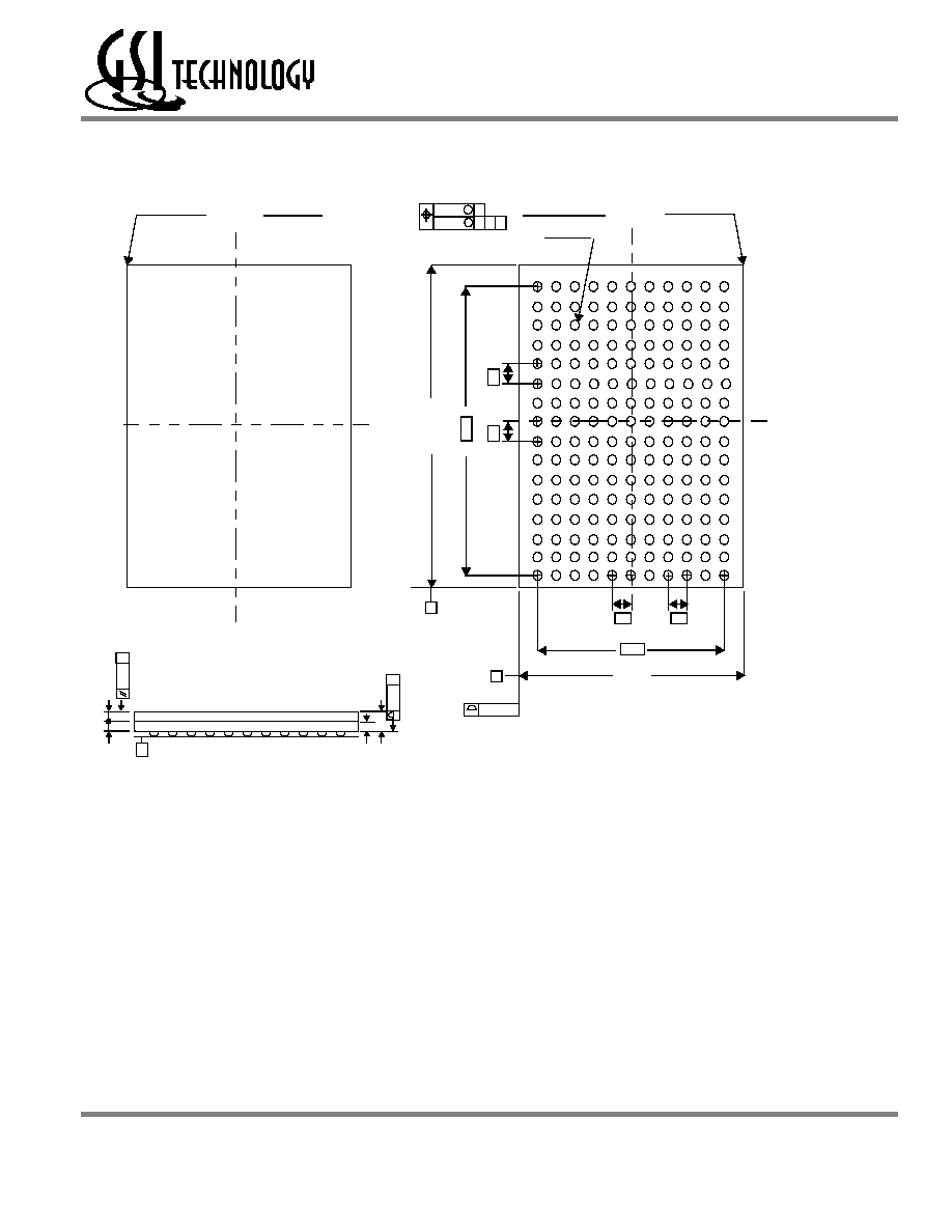
Package Dimensions--165-Bump FPBGA (Package D)
A
B
C
D
E
F
G
H
I
J
K
L
M
N
P
R
A
B
C
D
E
F
G
H
I
J
K
L
M
N
P
R
1 2 3 4 5 6 7 8 9 10 11
11 10 9 8 7 6 5 4 3 2 1
A1 CORNER
TOP VIEW
A1 CORNER
BOTTOM VIEW
1.0
1.0
10.0
1.
0
1.
0
14
.
0
13±0.07
15
±0
.0
7
A
B
0.20(4x)
ÿ0.10
ÿ0.25
C
C A B
M
M
ÿ0.40~0.50 (165x)
C
SEATING PLANE
0.
15
C
0.
25
~0.
4
0
1.
20 MAX.
0.
45±0.
05
0.
25
C
(0
.2
6)

Rev: 1.03a 9/2002
35/38
© 2001, Giga Semiconductor, Inc.
Specifications cited are subject to change without notice. For latest documentation see http://www.gsitechnology.com.
GS88218/36AB/D-250/225/200/166/150/133
Package Dimensions--119-Pin PBGA
A
B
Pin 1
Corner
K
E
F
CT
A
B
C
D
E
F
G
H
J
K
L
M
N
P
R
T
U
G
S
D
1
2
3
4
5
6
7
Package Dimensions--119-Pin PBGA
Unit: mm
Symbol
Description
Min. Nom. Max
A
Width
13.9
14.0
14.1
B
Length
21.9
22.0
22.1
C
Package Height (including ball)
1.73
1.86
1.99
D
Ball Size
0.60
0.75
0.90
E
Ball Height
0.50
0.60
0.70
F
Package Height (excluding balls) 1.16
1.26
1.36
G
Width between Balls
1.27
K
Package Height above board
0.65
0.70
0.75
R
Width of package between balls
7.62
S
Length of package between balls
20.32
T
Variance of Ball Height
0.15
Bottom View
R
Top View
Side View
A
B
C
D
E
F
G
H
J
K
L
M
N
P
R
T
U
Rev: 1.03a 9/2002
36/38
© 2001, Giga Semiconductor, Inc.
Specifications cited are subject to change without notice. For latest documentation see http://www.gsitechnology.com.
GS88218/36AB/D-250/225/200/166/150/133
Ordering Information for GSI Synchronous Burst RAMs
Org
Part Number
1
Type
Package
Speed
2
(MHz/ns)
T
A
3
Status
512K x 18
GS88218AB-250
Pipeline/Flow Through
119 BGA
250/5.5
C
512K x 18
GS88218AB-225
Pipeline/Flow Through
119 BGA
225/6
C
512K x 18
GS88218AB-200
Pipeline/Flow Through
119 BGA
200/6.5
C
512K x 18
GS88218AB-166
Pipeline/Flow Through
119 BGA
166/7
C
512K x 18
GS88218AB-150
Pipeline/Flow Through
119 BGA
150/7.5
C
512K x 18
GS88218AB-133
Pipeline/Flow Through
119 BGA
133/8.5
C
256K x 36
GS88236AB-250
Pipeline/Flow Through
119 BGA
250/5.5
C
256K x 36
GS88236AB-225
Pipeline/Flow Through
119 BGA
225/6
C
256K x 36
GS88236AB-200
Pipeline/Flow Through
119 BGA
200/6.5
C
256K x 36
GS88236AB-166
Pipeline/Flow Through
119 BGA
166/7
C
256K x 36
GS88236AB-150
Pipeline/Flow Through
119 BGA
150/7.5
C
256K x 36
GS88236AB-133
Pipeline/Flow Through
119 BGA
133/8.5
C
512K x 18
GS88218AB-250I
Pipeline/Flow Through
119 BGA
250/5.5
I
512K x 18
GS88218AB-225I
Pipeline/Flow Through
119 BGA
225/6
I
512K x 18
GS88218AB-200I
Pipeline/Flow Through
119 BGA
200/6.5
I
512K x 18
GS88218AB-166I
Pipeline/Flow Through
119 BGA
166/7
I
512K x 18
GS88218AB-150I
Pipeline/Flow Through
119 BGA
150/7.5
I
512K x 18
GS88218AB-133I
Pipeline/Flow Through
119 BGA
133/8.5
I
256K x 36
GS88236AB-250I
Pipeline/Flow Through
119 BGA
250/5.5
I
256K x 36
GS88236AB-225I
Pipeline/Flow Through
119 BGA
225/6
I
256K x 36
GS88236AB-200I
Pipeline/Flow Through
119 BGA
200/6.5
I
256K x 36
GS88236AB-166I
Pipeline/Flow Through
119 BGA
166/7
I
256K x 36
GS88236AB-150I
Pipeline/Flow Through
119 BGA
150/7.5
I
256K x 36
GS88236AB-133I
Pipeline/Flow Through
119 BGA
133/8.5
I
512K x 18
GS88218AD-250
Pipeline/Flow Through
165 BGA
250/5.5
C
512K x 18
GS88218AD-225
Pipeline/Flow Through
165 BGA
225/6
C
512K x 18
GS88218AD-200
Pipeline/Flow Through
165 BGA
200/6.5
C
512K x 18
GS88218AD-166
Pipeline/Flow Through
165 BGA
166/7
C
512K x 18
GS88218AD-150
Pipeline/Flow Through
165 BGA
150/7.5
C
512K x 18
GS88218AD-133
Pipeline/Flow Through
165 BGA
133/8.5
C
Notes:
1. Customers requiring delivery in Tape and Reel should add the character "T" to the end of the part number. Example: GS88236A-100IT.
2. The speed column indicates the cycle frequency (MHz) of the device in Pipeline mode and the latency (ns) in Flow Through mode. Each
device is Pipeline/Flow Through mode-selectable by the user.
3. T
A
= C = Commercial Temperature Range. T
A
= I = Industrial Temperature Range.
4. GSI offers other versions this type of device in many different configurations and with a variety of different features, only some of which
are covered in this data sheet. See the GSI Technology web site (www.gsitechnology.com) for a complete listing of current offerings

Rev: 1.03a 9/2002
37/38
© 2001, Giga Semiconductor, Inc.
Specifications cited are subject to change without notice. For latest documentation see http://www.gsitechnology.com.
GS88218/36AB/D-250/225/200/166/150/133
256K x 36
GS88236AD-250
Pipeline/Flow Through
165 BGA
250/5.5
C
256K x 36
GS88236AD-225
Pipeline/Flow Through
165 BGA
225/6
C
256K x 36
GS88236AD-200
Pipeline/Flow Through
165 BGA
200/6.5
C
256K x 36
GS88236AD-166
Pipeline/Flow Through
165 BGA
166/7
C
256K x 36
GS88236AD-150
Pipeline/Flow Through
165 BGA
150/7.5
C
256K x 36
GS88236AD-133
Pipeline/Flow Through
165 BGA
133/8.5
C
512K x 18
GS88218AD-250I
Pipeline/Flow Through
165 BGA
250/5.5
I
512K x 18
GS88218AD-225I
Pipeline/Flow Through
165 BGA
225/6
I
512K x 18
GS88218AD-200I
Pipeline/Flow Through
165 BGA
200/6.5
I
512K x 18
GS88218AD-166I
Pipeline/Flow Through
165 BGA
166/7
I
512K x 18
GS88218AD-150I
Pipeline/Flow Through
165 BGA
150/7.5
I
512K x 18
GS88218AD-133I
Pipeline/Flow Through
165 BGA
133/8.5
I
256K x 36
GS88236AD-250I
Pipeline/Flow Through
165 BGA
250/5.5
I
256K x 36
GS88236AD-225I
Pipeline/Flow Through
165 BGA
225/6
I
256K x 36
GS88236AD-200I
Pipeline/Flow Through
165 BGA
200/6.5
I
256K x 36
GS88236AD-166I
Pipeline/Flow Through
165 BGA
166/7
I
256K x 36
GS88236AD-150I
Pipeline/Flow Through
165 BGA
150/7.5
I
256K x 36
GS88236AD-133I
Pipeline/Flow Through
165 BGA
133/8.5
I
Org
Part Number
1
Type
Package
Speed
2
(MHz/ns)
T
A
3
Status
Notes:
1. Customers requiring delivery in Tape and Reel should add the character "T" to the end of the part number. Example: GS88236A-100IT.
2. The speed column indicates the cycle frequency (MHz) of the device in Pipeline mode and the latency (ns) in Flow Through mode. Each
device is Pipeline/Flow Through mode-selectable by the user.
3. T
A
= C = Commercial Temperature Range. T
A
= I = Industrial Temperature Range.
4. GSI offers other versions this type of device in many different configurations and with a variety of different features, only some of which
are covered in this data sheet. See the GSI Technology web site (www.gsitechnology.com) for a complete listing of current offerings

Rev: 1.03a 9/2002
38/38
© 2001, Giga Semiconductor, Inc.
Specifications cited are subject to change without notice. For latest documentation see http://www.gsitechnology.com.
GS88218/36AB/D-250/225/200/166/150/133
9Mb Sync SRAM Datasheet Revision History
DS/DateRev. Code: Old;
New
Types of Changes
Format or Content
Page;Revisions;Reason
88218A_r1
∑ Creation of new datasheet
88218A_r1_01
Content
∑ Updated AC Characteristics table
∑ Updated FT power numbers
∑ Updated Mb references from 8Mb to 9Mb
∑ Removed ByteSafe references
∑ Added 165-bump FPBGA package
∑ Updated AC Test Conditions table and removed Output Load
2 diagram
88218A_r1_01;
88218A_r1_02
Content
∑ Removed erroneous NBT references from ordering
information table
88218A_r1_02;
88218A_r1_03
Content
∑ Removed parity I/O bit designation from 165 BGA pinout
∑ Add SCN pin info to Mode Pin Functions table on page 12
∑ Removed BSR table
∑ Removed Preliminary banner
∑ Removed pin locations from pin description table