Features
l Low dark current
l High UV sensitivity
Applications
l Analytical instruments
l Color identification
l UV detection
P H O T O D I O D E
GaAsP photodiode
Schottky type for UV to visible range
G1126-02, G1127-02, G2119
s
General ratings / Absolute maximum ratings
Absolute maximum ratings
Active area
size
Effective
active
area
Reverse
voltage
V
R
Max.
Operating
temperature
Topr
Storage
temperature
Tstg
Type No.
Dimensional
outline/
Window
material
Package
(mm)
(mm
2
)
(V)
(∞C)
(∞C)
G1126-02
/Q *
TO-5
2.3 ◊ 2.3
5.2
G1127-02
/Q
TO-8
4.6 ◊ 4.6
21
G2119
/Q
Ceramic
10.1 ◊ 10.1
98
5
-10 to +60
-20 to +70
s
Electrical and optical characteristics (Typ. Ta=25
∞C, unless otherwise noted
)
Photo sensitivity
S
(A/W)
Spectral
response
range
Peak
sensitivity
wave-
length
p
Short circuit
current
Isc
100 lx
Dark
current
I
D
Max.
Temp.
coefficient
of
I
D
T
CID
Rise time
tr
V
R
=0 V
R
L
=1 k
Terminal
capacitance
Ct
V
R
=0 V
f=10 kHz
Shunt
resistance
Rsh
V
R
=10 mV
NEP
Type No.
(nm) (nm)
p
Hg
line
254 nm
GaP
LED
560 nm
He-Ne
laser
633 nm Min.
(µA)
Typ.
(µA)
V
4
=10 mV
(pA)
V
R
=1 V
(pA) (times/∞C)
(µs)
(pF)
Min.
(G)
Typ.
(G) (W/Hz
1/2
)
G1126-02
0.25 0.3
5
50
3.5
1800
2
15 5.8 ◊ 10
-15
G1127-02
0.9 1.2
10
100
12
7000
1
8
8.0 ◊ 10
-15
G2119
190 to 680 610 0.18 0.035 0.17 0.17
5
6
100 5000
1.07
55
25000 0.1 0.7 2.4 ◊ 10
-14
* Window material Q: quartz glass
GaAsP photodiode
G1126-02, G1127-02, G2119
LOAD RESISTANCE (
)
(Typ. Ta=25 ∞C, V
R
=0 V)
RISE TIME
10
3
10
4
10
2
100
ns
1
µs
10
ms
1
ms
100
µs
10
µs
10
5
10
6
G1127-02
G2119
G1126-02
REVERSE VOLTAGE (V)
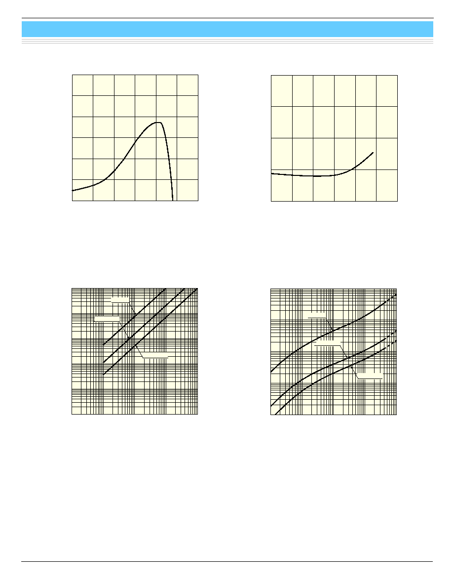
(Typ. Ta=25 ∞C)
DARK CURRENT
0.01
0.1
0.001
100
fA
1
pA
1
nA
100
pA
10
pA
1
10
G2119
G1127-02
G1126-02
0
0.1
0.05
0.15
0.2
0.25
0.3
190
400
600
WAVELENGTH (nm)
PHOTO SENSITIVITY (A/W)
800
(Typ. Ta=25 ∞C)
-0.5
0
+0.5
+1.0
+1.5
190
400
600
WAVELENGTH (nm)
TEMPERATURE COEFFICIENT
(%/
∞
C)
800
(Typ.)
s
s
s
s
s
Spectral response
KGPDB0034EA
s
s
s
s
s
Photo sensitivity temperature characteristic
KGPDB0035EA
s
s
s
s
s
Rise time vs. load resistance
KGPDB0036EA
s
s
s
s
s
Dark current vs. reverse voltage
KGPDB0037EA
GaAsP photodiode
G1126-02, G1127-02, G2119
G1126-02
s
s
s
s
s
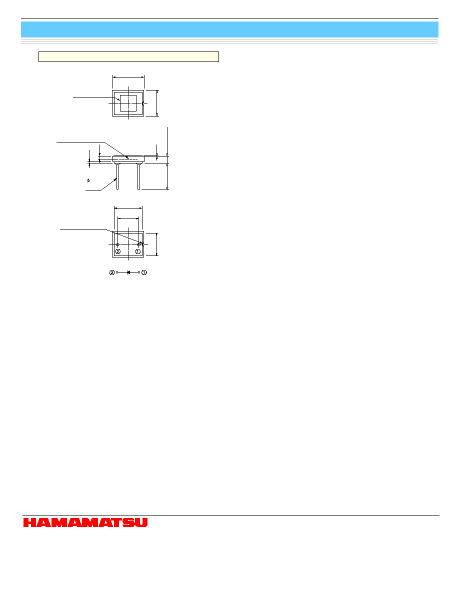
Dimensional outlines (unit: mm)
KGPDA0006EA
20
4.1 ± 0.2
2.9
0.45
LEAD
8.1 ± 0.1
WINDOW
5.9 ± 0.1
PHOTOSENSITIVE
SURFACE
9.1 ± 0.2
5.08 ± 0.2
CONNECTED
TO CASE
G1127-02
15
5.0 ± 0.2
1.9
0.45
LEAD
12.35 ± 0.1
13.9 ± 0.2
7.5 ± 0.2
WINDOW
10.5 ± 0.1
PHOTOSENSITIVE
SURFACE
MARK ( 1.4)
CONNECTED
TO CASE
KGPDA0007EA
s
s
s
s
s
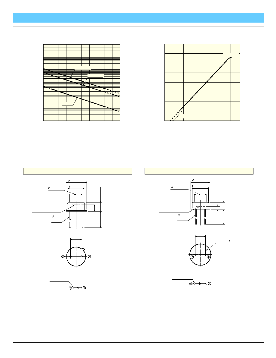
Shunt resistance vs. ambient temperature
KGPDB0038EA
s
s
s
s
s
Short circuit current linearity
KGPDB0008EA
AMBIENT TEMPERATURE (∞C)
(Typ. V
R
=10 mV)
SHUNT RESISTANCE
0
20
-20
10 M
1 G
100 M
10 T
1 T
100 G
10 G
40
60
80
G1127-02
G1126-02
G2119
INCIDENT LIGHT LEVEL (lx)
(Typ. Ta=25 ∞C, A light source fully illuminated)
OUTPUT CURRENT (A)
10
-14
10
-12
10
-10
10
-8
10
-6
10
-4
10
-2
10
-16
10
-16
10
-12
10
-14
10
0
10
-2
10
-4
10
-6
10
-8
10
-10
10
0
DEPENDENT ON NEP
R
L
=100
HAMAMATSU PHOTONICS K.K., Solid State Division
1126-1 Ichino-cho, Hamamatsu City, 435-8558 Japan, Telephone: (81) 053-434-3311, Fax: (81) 053-434-5184, http://www.hamamatsu.com
U.S.A.: Hamamatsu Corporation: 360 Foothill Road, P.O.Box 6910, Bridgewater, N.J. 08807-0910, U.S.A., Telephone: (1) 908-231-0960, Fax: (1) 908-231-1218
Germany: Hamamatsu Photonics Deutschland GmbH: Arzbergerstr. 10, D-82211 Herrsching am Ammersee, Germany, Telephone: (49) 08152-3750, Fax: (49) 08152-2658
France: Hamamatsu Photonics France S.A.R.L.: 8, Rue du Saule Trapu, Parc du Moulin de Massy, 91882 Massy Cedex, France, Telephone: 33-(1) 69 53 71 00, Fax: 33-(1) 69 53 71 10
United Kingdom: Hamamatsu Photonics UK Limited: 2 Howard Court, 10 Tewin Road, Welwyn Garden City, Hertfordshire AL7 1BW, United Kingdom, Telephone: (44) 1707-294888, Fax: (44) 1707-325777
North Europe: Hamamatsu Photonics Norden AB: Smidesv‰gen 12, SE-171 41 Solna, Sweden, Telephone: (46) 8-509-031-00, Fax: (46) 8-509-031-01
Italy: Hamamatsu Photonics Italia S.R.L.: Strada della Moia, 1/E, 20020 Arese, (Milano), Italy, Telephone: (39) 02-935-81-733, Fax: (39) 02-935-81-741
Information furnished by HAMAMATSU is believed to be reliable. However, no responsibility is assumed for possible inaccuracies or omissions.
Specifications are subject to change without notice. No patent rights are granted to any of the circuits described herein. ©2001 Hamamatsu Photonics K.K.
GaAsP photodiode
G1126-02, G1127-02, G2119
Cat. No. KGPD1005E01
Apr. 2001 DN
G2119
KGPDA0011EA
ANODE
TERMINAL MARK
0.5
LEAD
PHOTOSENSITIVE
SURFACE
16.5 ± 0.2
15.0 ± 0.15
ACTIVE AREA
2.15 ± 0.1
0.1
10.5
0.9
0.3
15.1 ± 0.3
12.5 ± 0.2
13.7 ± 0.3