 | –≠–ª–µ–∫—Ç—Ä–æ–Ω–Ω—ã–π –∫–æ–º–ø–æ–Ω–µ–Ω—Ç: G8925-XX | –°–∫–∞—á–∞—Ç—å:  PDF PDF  ZIP ZIP |

HAMAMATSU PHOTONICS K.K.
SOLID STATE DIVISION
1126-1 ICHINO-CHO,HAMAMATSU CITY 435-8558,JAPAN
TELEPHONE:053-434-3311
FAX:053-434-5184
OCD-B90754B
1/7
Jun. 2002
Hamamatsu Pigtail type,1.3 / 1.55um,10Gbps
InGaAs PIN-PD with Pre-Amplifier Module
Type No.G8925 series
FEATURES
∑ Ultra high speed response:10Gbps
∑ Four connector types are available ; SC/SPC-type(-x1), FC/SPC-type(-x2), MU-type(-x3),
LC-type(-x4).
∑ Low Power Supply Voltage:5V
∑ Differential Output
∑ Typical sensitivity:-18dBm
∑ Typical overload:0dBm
∑ High gain with AGC(Auto Gain Control)
GENERAL RATINGS (Fig.1)
Type No.
G8925-21
G8925-22
G8925-23
G8925-24
Connector type
SC(Fig.2)
FC(Fig.3)
MU(Fig.4)
LC(Fig.5)
Fiber type
Single-mode(9.5um/125um),
0.9mm dia. , 1m +0.2m/-0m
ABSOLUTE MAXIMUM RATINGS
(Ta=25deg.C)
Parameter
Symbol
Value
Unit
Remarks
Supply Voltage
Vcc
-0.7, +6
V
Reverse Voltage (PD)
V
R
20
V
Operating Temperature
Topr
-20 to +70
deg.C
Storage Temperature
Tstg
-40 to +85
deg.C
PRELIMINARY

HAMAMATSU PHOTONICS K.K.
SOLID STATE DIVISION
1126-1 ICHINO-CHO,HAMAMATSU CITY 435-8558,JAPAN
TELEPHONE:053-434-3311
FAX:053-434-5184
OCD-B90754B
2/7
ELECTRICAL AND OPTICAL CHARACTERISTICS
(Unless Otherwise Noted Ta=25deg.C,Vcc=Vpd=5V,Vee=0V, RL=50W)
Parameter
Symbol
Conditions
Min
Typ.
Max
Unit
Supply Current
Icc
Dark state, R
L
=•
--
78
--
mA
=1.3um
0.70
0.85
--
Photo Sensitivity
S
=1.55um
0.75
0.90
--
A/W
Output Bias Voltage
Vo
Dark state, R
L
=•
--
3.9
--
V
Bandwidth
fc
=1.55um, -3dB
--
8.5
--
GHz
Noise Equivalent
Power
NEP
Dark state, Single-ended,
10GHz
--
1.4
--
uWrms
Differential
transimpedance
Tz
RL=100ohm, f=100MHz
--
1.0
--
k
Min. Sensitivity
Pmin
10Gbps,NRZ
PRBS=2
23
-1,BER=10
-12
--
-18
--
dBm
Max. Overload
Pmax
10Gbps,NRZ
PRBS=2
23
-1,BER=10
-12
--
0
--
dBm
BLOCK DIAGRAM
43pF
470pF
V
100nF
PD
V
CC
GND
OUT+
Opt.IN
OUT-
CASE GND
470pF

HAMAMATSU PHOTONICS K.K.
SOLID STATE DIVISION
1126-1 ICHINO-CHO,HAMAMATSU CITY 435-8558,JAPAN
TELEPHONE:053-434-3311
FAX:053-434-5184
OCD-B90754B
3/7
DIMENSIONAL OUTLINE
Unit:mm, Unless otherwise noted: ±0.2
PIN CONNECTION
#1,3,6,8 GND
#2 Vpd
#4 Vout+
#5 Vout-
#7 Vcc
Fig.3 G8925-22(Connector type:FC)
Fig.1 G8925-2x
Fig.2 G8925-21(Connectortype:SC)
JIS C5970
FC CONNECTOR
JIS C5973
SC CONNECTOR
ANSI/TIA/EIA 604-10
LC CONNECTOR(BTW)
Fig.4 G8925-23(Connector type:MU)
JIS C5983
MU CONNECTOR
Fig.5 G8925-24(Connector type:LC)
7.5
8.0
2-2.2
5.5
6.8
5.0
6.0
3
10.96
2.1
Le
ad 2
,
7-0.3
Le
ad
1,3
,
6,8-0.5
3-
0.9
Le
ad 4,5-0.2
0.
9
4
3-
0.9
4.6
13
.
4
9.2
3.5
5.
5
(25)
(2.6)
0.7

HAMAMATSU PHOTONICS K.K.
SOLID STATE DIVISION
1126-1 ICHINO-CHO,HAMAMATSU CITY 435-8558,JAPAN
TELEPHONE:053-434-3311
FAX:053-434-5184
OCD-B90754B
4/7
OPERATING CIRCUIT EXAMPLE
FREQUENCY CHARACTERISTICS
Fig.7
Vcc=5V
Vee=GND
Opt. In
Vout-
0.1F
Tester or Post Amp.
0.1F
50
50
Coaxial
Cable
0.1F
Vout+
Vpd
0.1F
Fig. 6
S21
-10
-5
0
5
10
15
20
25
30
0
2
4
6
8
10
12
14
16
18
20
Frequency (GHz)
Gain (dB)
Vout-
Vout+
Vcc=Vpd=5V
Pin = -6dBm
HAMAMATSU PHOTONICS K.K.
SOLID STATE DIVISION
1126-1 ICHINO-CHO,HAMAMATSU CITY 435-8558,JAPAN
TELEPHONE:053-434-3311
FAX:053-434-5184
OCD-B90754B
5/7
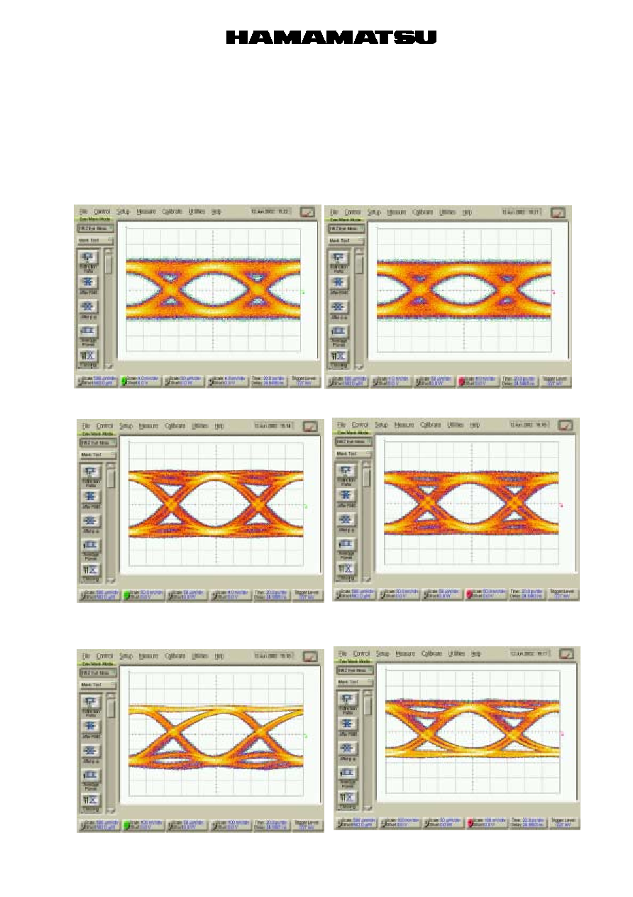
EYE DIAGRAM
Bit rate = 10Gbps, PN=23, NRZ
Extinction ratio = 13dB
Vcc=Vpd=5V, Resposivity = 0.9A/W
Fig.8 Pin = -18dBm 4mV/div. 20ps/div
Fig.9 Pin = -6dBm 50mV/div. 20ps/div
Fig.10 Pin = -1dBm 100mV/div. 20ps/div
Vout+
Vout+
Vout+
Vout-
Vout-
Vout-

HAMAMATSU PHOTONICS K.K.
SOLID STATE DIVISION
1126-1 ICHINO-CHO,HAMAMATSU CITY 435-8558,JAPAN
TELEPHONE:053-434-3311
FAX:053-434-5184
OCD-B90754B
6/7
BIT ERROR RATE
Bit rate = 10Gbps, PN=23, NRZ
Extinction ratio = 13dB
Vcc=5V, Resposivity = 0.9A/W
Fig. 11
1E-12
1E-11
1E-10
1E-09
1E-08
1E-07
1E-06
1E-05
1E-04
1E-03
-24 -23 -22 -21 -20 -19 -18 -17 -16 -15 -14
Average Power (dBm)
B
i
t
E
r
ro
r
R
a
t
e
Vpd=5V
Vpd=9V

HAMAMATSU PHOTONICS K.K.
SOLID STATE DIVISION
1126-1 ICHINO-CHO,HAMAMATSU CITY 435-8558,JAPAN
TELEPHONE:053-434-3311
FAX:053-434-5184
OCD-B90754B
7/7
PRECAUTION FOR HANDLING
1. This module may be damaged or its performance may deteriorate by such factors as
static electricity charges from the human body, surge voltages from measurement
equipment, leakage voltages from soldering irons, and packing materials. As a
countermeasure against static electricity, the device, operator, work place and
measuring jigs must all be set at the same potential.
2. The excessive stress should not be given to the leads during assembly or operation,
and a sufficient care should be taken for it. This is for avoiding deterioration of optical
coupling efficiency.
3. The basic material used in this type of Photodiode(PD) is InGaAs (Indium Galium
Arsenide) which may be hazardous to the health if handled improperly. It is therefore
strongly suggested that the PD be not physically disintegrated (grinding or crushing
etc.) or chemically decomposed (melting or vaporizing etc.). The PD must not be disposed
of without advice from specialists.