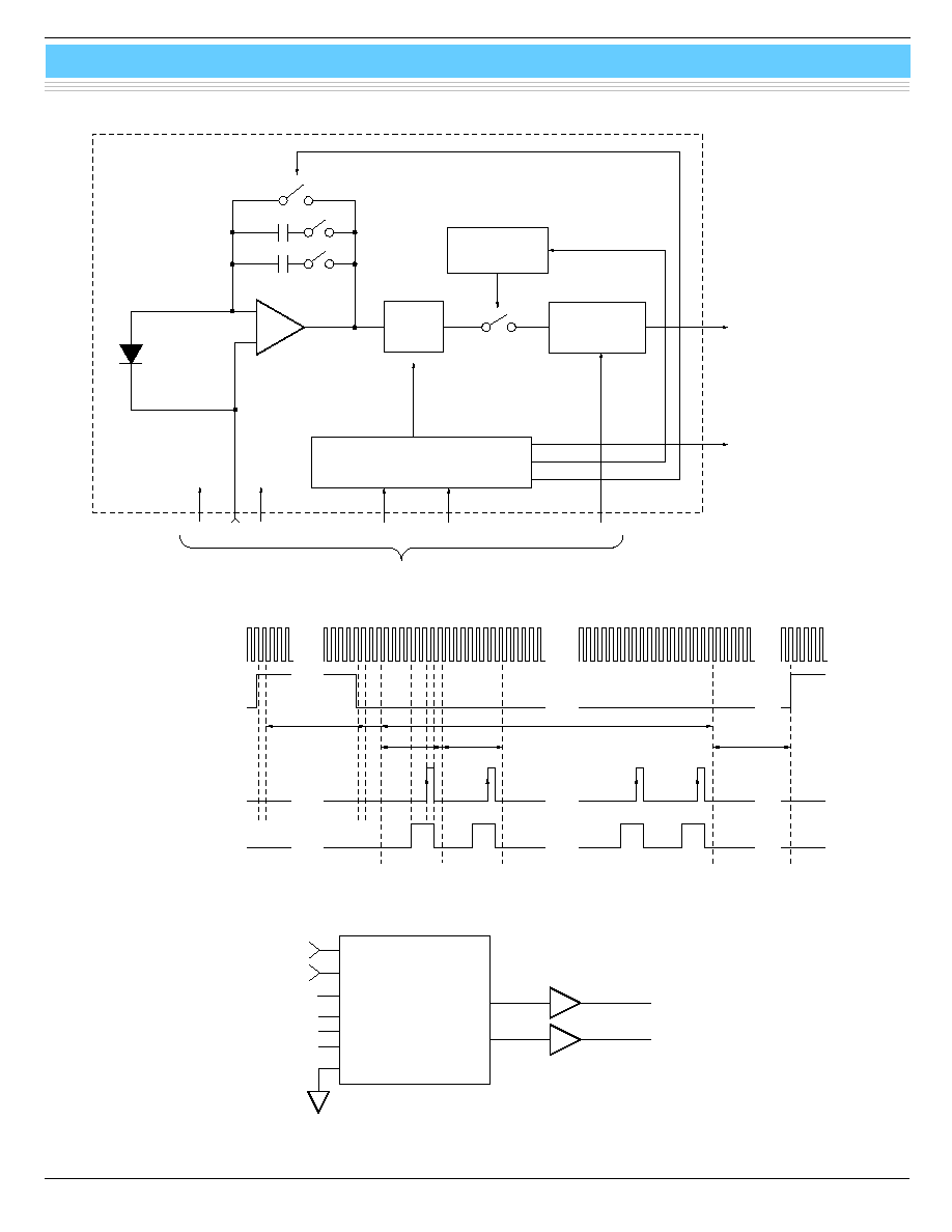
G9211 to G9214/G9205 to G9208 series InGaAs linear image sensors are specifically designed for near infrared multichannel spectrophotometry.
These linear image sensors consist of an InGaAs photodiode array, a charge amplifier array, an offset compensation circuit, a shift register and a
timing generator formed on a CMOS chip. The charge amplifier array is made up of CMOS transistors connected to each pixel of the InGaAs
photodiode array. Signals from each pixel are read out in charge integration mode to achieve high sensitivity and stable operation in the near
infrared spectral range. The package is hermetically sealed for high reliability.
Signal processing circuits on the CMOS chip allow selecting a feedback capacitance (Cf) of 10 pF or 0.5 pF by using an external voltage input.
The image sensor operates over a wide dynamic range when Cf=10 pF and delivers high gain when Cf=0.5 pF.
I M A G E S E N S O R
InGaAs linear image sensor
Near infrared image sensors (0.9 to 1.67 µm / 2.55 µm)
G9211 to G9214/G9205 to G9208 series
Features
l
Wide dynamic range
l
Low noise and low dark current
l
Selectable gain
l
Anti-saturation circuit
l
CDS circuit *
1
l
Offset compensation circuit
l
Simple operation (by built-in timing generator) *
2
l
High resolution: 25 µm pitch (512 ch)
l
Low cross-talk
l
256 ch: 1 video line
512 ch: 2 video lines
Applications
l
Near infrared multichannel spectrophotometry
l
Radiation thermometry
l
Non-destructive inspection
Related products
l
InGaAs multichannel detector head C8061-01, C8062-01
l
Multichannel detector head controller C7557
0.5
1.0
1.5
2.0
2.5
3.0
0
0.5
1.0
1.5
WAVELENGTH (µm)
PHOTO SENSITIVITY
(A/W)
(Typ.)
T=25 ∞C
T= -10 ∞C (G9208-256W: T= -20 ∞C)
G9211 TO
G9214 SERIES
G9208-256W
s
Spectral response
KMIRB0022EA
*1: CDS (Correlated Double Sampling) circuit
A major source of noise in charge amplifiers is the reset noise gen-
erated when the integration capacitance is reset. A CDS circuit greatly
reduces this reset noise by holding the signal immediately after re-
set to find the
noise differential
.
*2: Timing generator
Different signal timings must be properly set in order to operate a
shift register. In conventional image sensor operation, external PLDs
(Programmable Logic Devices) are used to input the required timing
signals. However, G9211 to G9214/G9205 to G9208 series image
sensors internally generate all timing signals on the CMOS chip just
by supplying CLK and RESET pulses. This makes it simple to set the
timings.
*3: Percentage of defective pixels
If your application requires sensors with no defective pixels, please
select G9201 series.
1
s Selection guide
Type No.
Cooling
Num ber of
pixels
Pixel pitch
(µm )
Pixel size
[µm (H) ◊ µm (V)]
Spectral
response range
(µm )
Defective
pixel
G9211-256S
256
50
50 ◊ 250
G9212-512S
512
25
25 ◊ 250
G9213-256S
256
50
50 ◊ 500
G9214-512S
One-stage
TE-cooled
512
25
25 ◊ 500
0.9 to 1.70
1 % Max. *
3
G9205-256W
0.9 to 1.85
G9206-256W
0.9 to 2.05
G9207-256W
0.9 to 2.25
G9208-256W
Two-stage
TE-cooled
256
50
50 ◊ 250
0.9 to 2.55
5 % Max.

InGaAs linear image sensor
G9211 to G9214/G9205 to G9208 series
2
s Absolute maximum ratings
Parameter
Symbol
Value
Unit
Clock pulse voltage
V
5.5
V
Operating temperature *
1
Topr
-40 to +70
∞C
Storage temperature *
1
Tstg
-40 to +85
∞C
*1: Non condensation
s Electrical characteristics (Ta=25 ∞C, V
=5 V)
Parameter
Symbol
Min.
Typ.
Max.
Unit
Vdd
4.5
5.0
5.5
Supply voltage
Vref
-
1.26
-
V
Ground
Vss
-
0
-
V
Element bias
INP
3.5
4.5
4.6
V
Clock frequency
f
0.1
-
4
MHz
high
V
- 0.5
V
V
+ 0.5
V
Clock pulse voltage
low
V
0
0
0.4
V
tr
Clock pulse rise/fall times
tf
0
20
100
ns
Clock pulse width
tpw
200
-
-
ns
high
V
- 0.5
V
V
+ 0.5
V
Reset pulse voltage
low
V (RES)
0
0
0.4
V
tr (RES)
Reset pulse rise/fall times
tf (RES)
0
20
100
ns
Reset pulse width
tpw (RES)
6000
-
-
ns
high
V
H
-
4.1
-
Video output voltage
low
V
L
-
1.26
-
V
Data rate
f
V
-
f/8
-
Hz
s Electrical and optical characteristics (G9211 to G9214 series: T=25 ∞C, G9205 to G9208 series: T= -20 ∞C)
G9211 to G9214 series
G9205 to G9208 series
Parameter
Symbo
l
Min.
Typ.
Max.
Min.
Typ.
Max.
Unit
G9205
-
1.75
-
G9206
-
1.95
-
G9207
-
2.05
-
Peak sensitivity wavelength
p
-
1.55
-
G9208
-
2.3
-
µm
Saturation charge
*2
Qsat
-
30
-
-
30
-
pC
RMS noise voltage
(Readout noise)
N
-
180
300
-
180
300
µVrms
Photo response non-uniformity
PRNU
-
-
±5
*3
-
-
±10
*4
%
*2: V
=5 V, Cf=10 pF
*3: 50 % of saturation, integration time: 10 ms, after dark output subtraction, excluding first and last pixels.
*4: 50 % of saturation, integration time: 3 ms, after dark output subtraction, excluding first and last pixels.
Dark current characteristics (T=25 ∞C)
Parameter
Symbol
Min.
Typ.
Max.
Unit
G9211-256S
-
2
10
G9212-512S
-
1
5
G9213-256S
-
4
20
G9214-512S
-
1
5
G9205-256W
*5
-
15
60
G9206-256W
*5
-
30
120
G9027-256W
*5
-
200
800
G9208-256W
*5
I
D
-
500
2000
pA
*5: T
D
= -20 ∞C
InGaAs linear image sensor
G9211 to G9214/G9205 to G9208 series
1.0 ± 0.2
1 2
14
28
15
10.2 ± 0.15
3.0 ± 0.15
25.4 ± 0.15
22.9 ± 0.15
63.5 ± 0.15
53.3 ± 0.15
38.1 ± 0.15
35.6 ± 0.15
20.3 ± 0.15
A
B
(28 ◊) 2.54
(28 ◊) 0.46
6.4 ± 1
27.2 ± 0.15
INDEX MARK
ONE-STAGE TE-COOLED
TWO-STAGE TE-COOLED
6.15
3.6
A
B
7.25
4.5
HAMAMATSU PHOTONICS K.K., Solid State Division
1126-1 Ichino-cho, Hamamatsu City, 435-8558 Japan, Telephone: (81) 053-434-3311, Fax: (81) 053-434-5184, http://www.hamamatsu.com
U.S.A.: Hamamatsu Corporation: 360 Foothill Road, P.O.Box 6910, Bridgewater, N.J. 08807-0910, U.S.A., Telephone: (1) 908-231-0960, Fax: (1) 908-231-1218
Germany: Hamamatsu Photonics Deutschland GmbH: Arzbergerstr. 10, D-82211 Herrsching am Ammersee, Germany, Telephone: (49) 08152-3750, Fax: (49) 08152-2658
France: Hamamatsu Photonics France S.A.R.L.: 8, Rue du Saule Trapu, Parc du Moulin de Massy, 91882 Massy Cedex, France, Telephone: 33-(1) 69 53 71 00, Fax: 33-(1) 69 53 71 10
United Kingdom: Hamamatsu Photonics UK Limited: 2 Howard Court, 10 Tewin Road, Welwyn Garden City, Hertfordshire AL7 1BW, United Kingdom, Telephone: (44) 1707-294888, Fax: (44) 1707-325777
North Europe: Hamamatsu Photonics Norden AB: Smidesv‰gen 12, SE-171 41 Solna, Sweden, Telephone: (46) 8-509-031-00, Fax: (46) 8-509-031-01
Italy: Hamamatsu Photonics Italia S.R.L.: Strada della Moia, 1/E, 20020 Arese, (Milano), Italy, Telephone: (39) 02-935-81-733, Fax: (39) 02-935-81-741
Information furnished by HAMAMATSU is believed to be reliable. However, no responsibility is assumed for possible inaccuracies or omissions.
Specifications are subject to change without notice. No patent rights are granted to any of the circuits described herein. ©2003 Hamamatsu Photonics K.K.
Cat. No. KMIR1011E02
Jun. 2003 DN
s
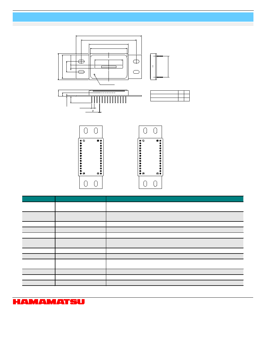
Dimensional outline (unit: mm)
KMIRA0011EA
KMIRC0013EA
s
Pin connection (top view)
TE +
THERM
THERM
CASE
RESET
TE -
Vdd
Vss
INP
CLK
Vref
VIDEO
Cf SELECT
AD-TRIG
256 PIXELS
512 PIXELS
TE +
THERM
THERM
CASE
RESET-ODD
TE -
Vdd
Vss
INP
CLK-ODD
Vref
VIDEO-ODD
Cf SELECT
AD-TRIG-ODD
RESET-EVEN
AD-TRIG-EVEN
CLK-EVEN
VIDEO-EVEN
Terminal name
Input/Output
Function and recommended connection
CLK
Input
(CMOS logic compatible)
Clock pulse for operating the CMOS shift register
RESET
Input
(CMOS logic compatible)
Reset pulse for initializing the feedback capacitance in the charge amplifier
formed on the CMOS chip. The width of the reset pulse is integration time.
Vdd
Input
Supply voltage for operating the signal processing circuit on the CMOS chip.
Vss
-
Ground for the signal processing circuit on the CMOS chip.
INP
Input
Reset voltage for the charge amplifier array on the CMOS chip.
Cf SELECT
Input
Voltage that determines the feedback capacitance (Cf) on the CMOS chip.
Cf=10 pF at 0 V, and Cf=0.5 pF at 5 V.
CASE
-
This terminal is electrically connected to the package.
THERM
-
Thermistor for monitoring temperature inside the package.
TE+, TE-
-
Power supply terminal for the thermoelectric cooler that cools the photodiode
array. No connection for room temperature operation type.
AD-TRIG
Output
Digital signal for AD conversion; positive polarity
VIDEO
Output
Analog video signal; positive polarity
Vref
Input
Reset voltage for the offset compensation circuit at the CMOS chip
4