Features
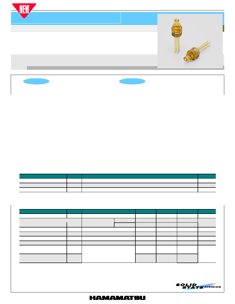
l 1.25 mm sleeve type ROSA (Receiver Optical
Sub-Assembly)
l High-speed response: 2.5 Gbps
l High gain with AGC (Auto Gain Control): 0.65 V/mW (-17 dBm)
l Low power supply voltage: 3.3 V, 5 V
l Differential output
l Sensitivity: 1 to -22 dBm Typ.
Applications
l Gigabit Ethernet
l Fiber channel
P H O T O D I O D E
ROSA type, 850 nm, 2.5 Gbps
G9286-14
GaAs PIN photodiode with preamp
PRELIMINARY DATA
Mar. 2003
1
I Absolute maximum ratings (Ta=25 ∞C)
Parameter
Symbol
Value
Unit
Supply voltage
Vcc
-0.5, +6
V
Operating temperature
Topr
-20 to +70 *
1
∞C
Storage temperature
Tstg
-40 to +85 *
1
∞C
*1: No condensation
I Electrical and optical characteristics
(Ta=25 ∞C, Vcc=3.3 V or 5 V, Vee=GND, R
L
=50 W, l=850 nm, unless otherwise noted)
Parameter
Symbol
Condition
Min.
Typ.
Max.
Unit
Photo sensitivity *
2,
*
3
S
Pin= -17 dBm *
3
(f=100 MHz)
0.4
0.65
-
V/mW
Vcc=3.3 V
-
35
50
Supply current
Icc
Dark state, R
L
=•
Vcc=5 V
-
42
-
mA
Output bias voltage
Vo
Dark state, R
L
=•, Vcc=3.3 V
-
3.0
-
V
Cut-off frequency *
2,
*
3
fc
Pin= -17 dBm, -3 dB
-
1900
-
MHz
Low cut-off frequency *
2
fc-L
Pin= -17 dBm, -3 dB
-
30
-
kHz
Noise equivalent power *
2,
*
3
NEP
Dark state, to 1866 MHz
-
800
-
nWrms
Minimum receivable
sensitivity
Pmin
-
-22
-
Maximum receivable
sensitivity
Pmax
2.5 Gbps, NRZ,
PN=23, BER=10
-10
,
Extinction ratio=9 dB
-
+1
-
dBm
*2: Output: Capacitive coupling
*3: Single-ended (Vout+) measurement

GaAs PIN photodiode with preamp
G9286-14
HAMAMATSU PHOTONICS K.K., Solid State Division
1126-1 Ichino-cho, Hamamatsu City, 435-8558 Japan, Telephone: (81) 053-434-3311, Fax: (81) 053-434-5184, http://www.hamamatsu.com
U.S.A.: Hamamatsu Corporation: 360 Foothill Road, P.O.Box 6910, Bridgewater, N.J. 08807-0910, U.S.A., Telephone: (1) 908-231-0960, Fax: (1) 908-231-1218
Germany: Hamamatsu Photonics Deutschland GmbH: Arzbergerstr. 10, D-82211 Herrsching am Ammersee, Germany, Telephone: (49) 08152-3750, Fax: (49) 08152-2658
France: Hamamatsu Photonics France S.A.R.L.: 8, Rue du Saule Trapu, Parc du Moulin de Massy, 91882 Massy Cedex, France, Telephone: 33-(1) 69 53 71 00, Fax: 33-(1) 69 53 71 10
United Kingdom: Hamamatsu Photonics UK Limited: 2 Howard Court, 10 Tewin Road, Welwyn Garden City, Hertfordshire AL7 1BW, United Kingdom, Telephone: (44) 1707-294888, Fax: (44) 1707-325777
North Europe: Hamamatsu Photonics Norden AB: Smidesv‰gen 12, SE-171 41 Solna, Sweden, Telephone: (46) 8-509-031-00, Fax: (46) 8-509-031-01
Italy: Hamamatsu Photonics Italia S.R.L.: Strada della Moia, 1/E, 20020 Arese, (Milano), Italy, Telephone: (39) 02-935-81-733, Fax: (39) 02-935-81-741
Information furnished by HAMAMATSU is believed to be reliable. However, no responsibility is assumed for possible inaccuracies or omissions.
Specifications are subject to change without notice. No patent rights are granted to any of the circuits described herein. ©2003 Hamamatsu Photonics K.K.
Cat. No. KGPD1011E03
Apr. 2003 DN
2
I Eye diagram
KGPDA0020EA
I Photo sensitivity vs. average optical input power
KGPDB0055EA
I Bit error rate
I Dimensional outline
(unit: mm, unless otherwise noted: ±0.15)
-30
-25
-20
-15
-10
-5
0
0
1.5
0.5
1.0
AVERAGE OPTICAL INPUT POWER (dBm)
PHOTO SENSITIVITY
(V/mW)
(Typ. Ta=25 ∞C, Duty ratio=50 %, Pulse width=2 ns)
KGPDB0056EA
-27
-17
-18
-19
-20
-21
-22
-23
-24
-25
-26
10
-12
10
-3
10
-4
10
-5
10
-6
10
-7
10
-8
10
-9
10
-10
10
-11
AVERAGE OPTICAL INPUT POWER (dBm)
BIT ERROR RATIO
(Typ. Ta=25 ∞C, Bit rate=2.5 Gbps, Vcc=3.3 V, PN=23)
4.88
5.08
2.72
1.25
4.17 ± 0.05
5.94 ± 0.07
2.92
4.04 ± 0.05
1.27 ± 0.05
6.86 ± 0.5
4.64
3.38 ± 0.05
5.94 ± 0.07 0.3
2.95 ± 0.1
6.6
5.4
2.54
Vcc
Vout-
Vee
Vout+
Bit rate=2.5 Gbps. PN =23
=850 nm, Pin= -15 dBm, Vcc=3.3 V