
Spectral Response
UV LASER
SENSOR MODULE
H8496, H8497 series
FEATURES
OVER VIEW
UV Laser Sensor Modules provide high sensitivity in the VUV
to UV region. Excellent solar blind characteristics eliminate the
need for visual cut-off filters, thus extending the service life of
the module. The phototube is assembled in a compact, easy-
to-use TO-8 style package, along with a high voltage power
supply that operates by low voltage input.
The H8497 further incorporates an amplifier for voltage output.
GSolar Blind
GCompact
GLow Voltage Operation
GHigh Sensitivity in VUV Range
GHigh Speed Response
GHigh Stability
APPLICATIONS
GUV Laser Monitor
Excimer laser
YAG laser (4
: 266 nm, 5 : 213 nm)
GExcimer Lamp Monitor
GMercury Lamp Monitor
TPT B0020EA
PRELIMINARY
100
10
1
0.1
0.01
1
[H8497]
[H8496]
0.1
0.01
0.001
0.0001
100
150
200
250
WAVELENGTH (nm)
RADIANT SENSITIVITY (mA/W)
RADIANT SENSITIVITY (V/mW)
300
350
400
-21
-16
-11
-26

SELECTION GUIDE
GGENERAL
GH8496 series ..... Current output type (without an amplifier)
H8497 series ..... Voltage output type (with an amplifier)
SPECIFICATIONS
GH8496
GH8497
MAXIMUM RATINGS (Absolute Maximum Values)
GH8496
GH8497
Spectral Response
Wavelength of Maximum Response
Photocathode
Window Material
Weight
Material
Minimum Effective Area
Parameter
160 to 320
200
Cs-Te
8
Synthetic silica
-11
160 to 220
170
Diamond
6
Synthetic silica
-16
115 to 320
200
Cs-Te
8
MgF
2
Approx. 75
-21
115 to 220
160
Diamond
6
MgF
2
-26
nm
nm
--
mm
--
g
Unit
Supply Voltage
Peak Output Current
Average Output Current
Excimer Laser Measurement
Range F
2
Laser
A
Ambient Temperature
A Wavelength: 157 nm, Pulse width: 10 ns, Frequency: 1 kHz
NOTE:
Peak Power
Pulse Energy
Operating
Storage
Parameter
--
--
-11
--
--
+16
60
40
+5 to +40
-20 to +50
-16
3.3
33
-21
6
60
-26
V dc
mA
µA
W
nJ
∞C
∞C
Unit
Supply Voltage
Peak Output Voltage
B
Average Output Voltage
C
Ambient Temperature
B At input light pulse width: 800 ns
C CW light input
NOTE:
D At maximum response wavelength
NOTE:
E At maximum response wavelength and CW light input
NOTE:
Operating
Storage
Parameter
-11
±16
5
0.4
+5 to +40
-20 to +50
-16
-21
-26
V dc
V
V
∞C
∞C
Unit
Radiant Sensitivity
D
(Typ.)
Rise Time
Dark Current (Max.)
Output Signal Polarity
Recommended Operating Voltage
Parameter
22
-11
5
450
10
positive
+11.5 to +15.5
-16
22
-21
10
-26
mA/W
ps
pA
--
V
Unit
Radiant Sensitivity
E
(Typ.)
Offset Voltage (Max.)
Current Voltage Conversion Factor
Frequency Bandwidth
Output Signal Polarity
Recommended Operating Voltage
Parameter
0.22
-11
0.05
10
0.01
0 to 1 MHz
positive
±11.5 to ±15.5
-16
0.22
-21
0.10
-26
V/mW
mV
V/
µA
--
--
V
Unit
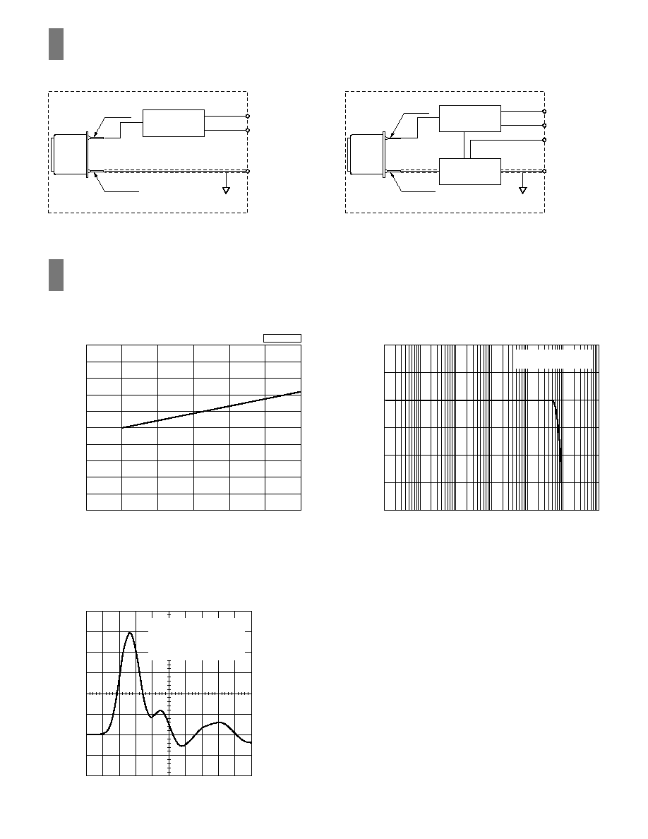
INTERNAL DIAGRAM
CHARACTERISTICS
GH8496
GH8497
GTemperature Characteristics
(Diamond Photocathode)
GPulse Linearity (H8496)
CATHODE
ANODE
HV POWER
SUPPLY
PHOTO-
TUBE
Vcc INPUT
(+11.5 V to +15.5 V)
Vee INPUT
(-11.5 V to -15.5 V)
GND
SIGNAL OUTPUT
I/V CONVERTOR
1.05
1.00
0.95
at 172 nm
20
25
30
35
AMBIENT TEMPERATURE (
∞C)
RELATIVE OUTPUT
40
45
50
GOutput Waveform (H8496)
CATHODE
ANODE
HV POWER
SUPPLY
PHOTO-
TUBE
Vcc INPUT
(+11.5 V to +15.5 V)
GND
SIGNAL OUTPUT
10
-20
-10
0
10
-6
10
-3
10
-5
10
-4
OUTPUT CURRENT (A)
DEVIATION (%)
10
-2
10
0
10
-1
PULSE WIDTH: 800 ns
FREQUENCY : 100 Hz
TIME (0.5 ns/div.)
OUTPUT VOLTAGE (20 mV/div.)
RISE TIME
FALL TIME
FWHM
LOAD RESISTANCE
LASER PULSE
: 450 ps
: 1100 ps
: 700 ps
: 50
: 50 ps
TPT B0023EB
TPT B0021EB
TPT B0022EB
TPT C0006EA
TPT C0007EA
TPT 1014E01
JUN. 2001 IP
Printed in Japan (1000)
Information furnished by HAMAMATSU is believed to be reliable. However, no responsibility is assumed for possible inaccuracies or omissions. Specifications are
subject to change without notice. No patent rights are granted to any of the circuits described herein. ©2001 Hamamatsu Photonics K.K
Subject to local technical requirements and regulations, availability of products included in this promotional material may vary. Please consult with our sales office.
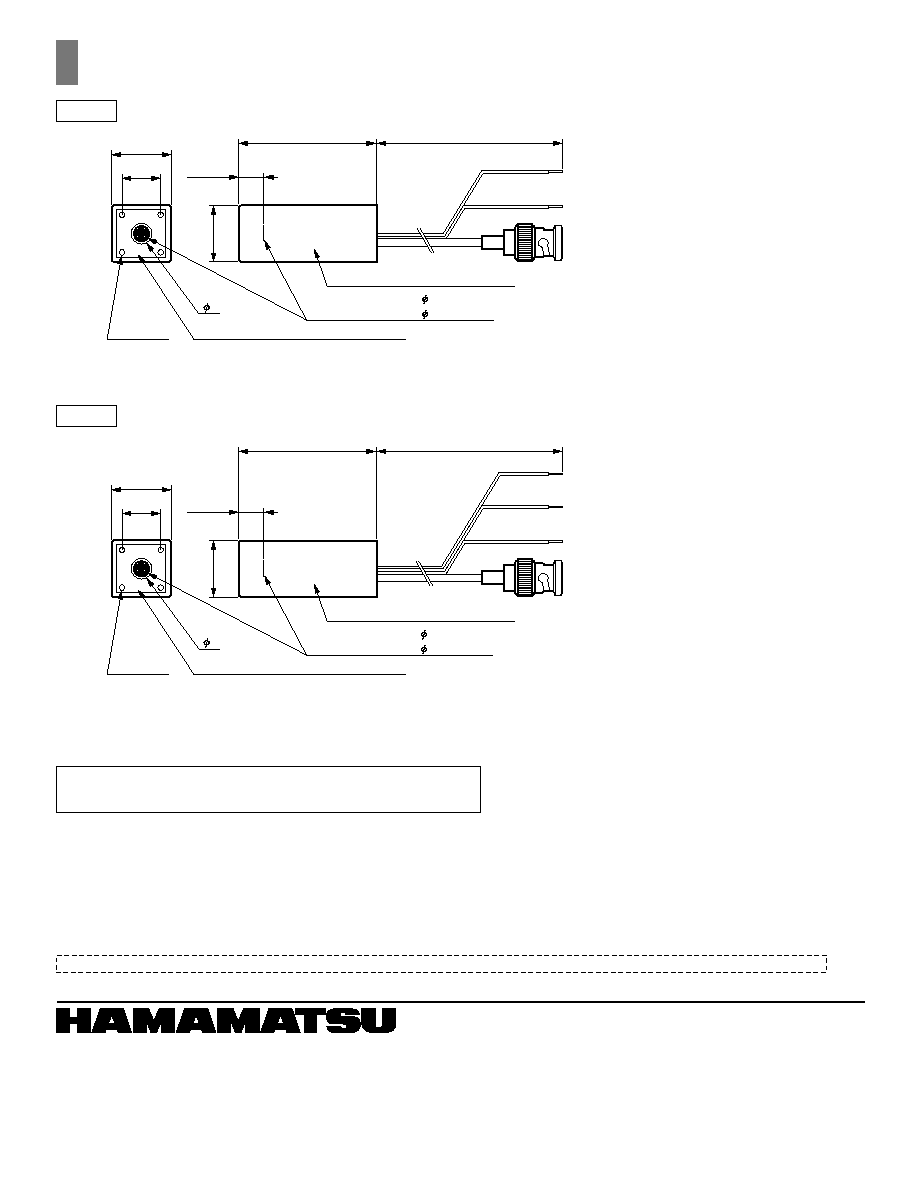
DIMENSIONAL OUTLINE
(Unit: mm)
HAMAMATSU PHOTONICS K.K., Electron Tube Center
314-5, Shimokanzo, Toyooka-village, Iwata-gun, Shizuoka-ken, 438-0193, Japan, Telephone: (81)539/62-5248, Fax: (81)539/62-2205
U.S.A.: Hamamatsu Corporation: 360 Foothill Road, P. O. Box 6910, Bridgewater. N.J. 08807-0910, U.S.A., Telephone: (1)908-231-0960, Fax: (1)908-231-1218 E-mail: usa@hamamatsu.com
Germany: Hamamatsu Photonics Deutschland GmbH: Arzbergerstr. 10, D-82211 Herrsching am Ammersee, Germany, Telephone: (49)8152-375-0, Fax: (49)8152-2658 E-mail: info@hamamatsu.de
France: Hamamatsu Photonics France S.A.R.L.: 8, Rue du Saule Trapu, Parc du Moulin de Massy, 91882 Massy Cedex, France, Telephone: (33)1 69 53 71 00, Fax: (33)1 69 53 71 10 E-mail: infos@hamamatsu.fr
United Kingdom: Hamamatsu Photonics UK Limited: 2 Howard Court, 10 Tewin Road Welwyn Garden City Hertfordshire AL7 1BW, United Kingdom, Telephone: 44-(0)1707-294888, Fax: 44(0)1707-325777 E-mail: info@hamamatsu.co.uk
North Europe: Hamamatsu Photonics Norden AB: Smidesv‰gen 12, SE-171-41 SOLNA, Sweden, Telephone: (46)8-509-031-00, Fax: (46)8-509-031-01 E-mail: info@hamamatsu.se
Italy: Hamamatsu Photonics Italia: S.R.L.: Strada della Moia, 1/E, 20020 Arese, (Milano), Italy, Telephone: (39)02-935 81 733, Fax: (39)02-935 81 741 E-mail: info@hamamatsu.it
HOMEPAGE URL http://www.hamamatsu.com
TPT A0029EA
TPT A0028EA
H8496
H8497
G Operate below 10
-1
Pa condition or under atmospheric pressure.
G Protect wires from UV light. UV light will degrade wires.
Handling precautions
14.0
±0.2
22.0
±0.5
22.0
±
0.5
9.2
±0.3
300
±20
50.0
±0.5
EFFECTIVE AREA
STEEL WITH NICKEL PLATING
8 (-11, -21)
6 (-16, -26)
8
4-M2 D: 4
ALUMINUM WITH NICKEL PLATING
AWG22 (RED)
: Vcc INPUT (+11.5 V to +15.5 V)
AWG22 (BLACK)
: GND
BNC
: SIGNAL OUTPUT
14.0
±0.2
22.0
±0.5
22.0
±
0.5
9.2
±0.3
300
±20
50.0
±0.5
EFFECTIVE AREA
STEEL WITH NICKEL PLATING
8 (-11, -21)
6 (-16, -26)
8
4-M2 D: 4
ALUMINUM WITH NICKEL PLATING
AWG22 (RED)
: Vcc INPUT (+11.5 V to +15.5 V)
AWG22 (BLUE)
: Vee INPUT (-11.5 V to -15.5 V)
AWG22 (BLACK)
: GND
BNC
: SIGNAL OUTPUT