PRELIMINARY
Electron Detection Unit
APPLICATIONS
FEATURES
H8770
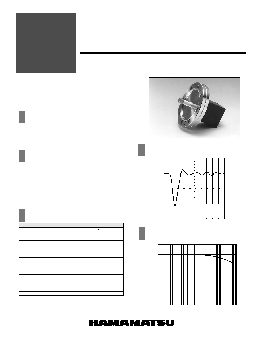
HAMAMATSU has introduced new Electron Detection Unit
H8770, consist of newly developed extremely fast decay
phosphor and high sensitivity compact PMT.
Decay time of the phosphor is faster than 1ns, and it can present
high speed electron detection.
Built-in PMT power supply, high speed amplifier and other
circuitry provide its easy operation.
GSemiconductor Inspection System
GScanning Electron Microscope (SEM)
GMass Spectrometer (MS)
GGeneral Electron Detection
Phosphor Life Characteristics
GFast Decay Phosphor: 720ps Typ.
GLong Life Phosphor: Low Degradation Against Electron
Irradiation
GHigh Sensitivity Compact PMT
GBuilt-in High Voltage Power Supply, Voltage Divider Circuit
for PMT and High Speed Amplifier (upto 150 MHz)
GVacuum Flange ICF114 is assembled (Custom assembly is
available upon request)
Parameter
Phosphor Effective Area
q
Type of Phosphor
Light Guide Material
Light Detector
Detectable Input Electron Energy Range
Electron-to-Voltage Conversion
PMT Gain Range
Built-in Amplifier Frequency Bandwidth
Maximum Output Voltage
Offset Voltage
Noise Level
Input Voltage
Input Current
Type of Vacuum Flange
Operating Temperature Range
Weight
NOTE: qOther dimension is available upon request.
wPlastic can be chosen. Custom design is also available.
eAt input electron energy : 6 keV, PMT gain: 1
◊ 10
4
rAdjustable by controll voltage (+1 V to +4 V) or externally
connected variable resistor.
tAt 50
load resistance
yWithout condensation
9 mm
Fast Decay Phosphor
Synthetic Silica
w
Photomultiplier tube
5 keV to 12 keV
10 V/
µA
e
1
◊ 10
2
to 1
◊10
6
r
DC to 150 MHz
-1.4 V
t
±10 mV Max.
20 mV
±15 V dc ±1 V dc
110 mA
ICF114
+5
∞C to +45 ∞C
y
1.46 kg
Description/Value
SPECIFICATIONS
TPMOB0157EA
Time Response
(Output Waveform)
TPMOB0152EA
TIME (2ns/div.)
RELA
TIVE OUTPUT
SIGNAL
RISE TIME
FALL TIME
FWHM
INPUT ELECTRON PULSE WIDTH
: 1.05 ns
: 1.38 ns
: 1.89 ns
: 100 ps
1.2
1
0.8
0.6
0.4
0.2
10
-5
10
-4
10
-3
10
-2
TOTAL ACCUMULATED INPUT CHARGE (C/cm
2
)
10
-1
10
0
0
RELA
TIVE OUTPUT
SIGNAL
INPUT ELECTRON ENERGY: 5 keV

TPMO0121E01
APR. 2002 IP
Information furnished by HAMAMATSU is believed to be reliable. However, no responsibility is assumed for possible inaccuracies or omissions. Specifications are
subject to change without notice. No patent rights are granted to any of the circuits described herein. ©2002 Hamamatsu Photonics K.K
Subject to local technical requirements and regulations, availability of products included in this promotional material may vary. Please consult with our sales office.
DIMENSIONAL OUTLINES
(Unit: mm)
HAMAMATSU PHOTONICS K.K., Electron Tube Center
314-5, Shimokanzo, Toyooka-village, Iwata-gun, Shizuoka-ken, 438-0193, Japan, Telephone: (81)539/62-5248, Fax: (81)539/62-2205
U.S.A.: Hamamatsu Corporation: 360 Foothill Road, P. O. Box 6910, Bridgewater. N.J. 08807-0910, U.S.A., Telephone: (1)908-231-0960, Fax: (1)908-231-1218 E-mail: usa@hamamatsu.com
Germany: Hamamatsu Photonics Deutschland GmbH: Arzbergerstr. 10, D-82211 Herrsching am Ammersee, Germany, Telephone: (49)8152-375-0, Fax: (49)8152-2658 E-mail: info@hamamatsu.de
France: Hamamatsu Photonics France S.A.R.L.: 8, Rue du Saule Trapu, Parc du Moulin de Massy, 91882 Massy Cedex, France, Telephone: (33)1 69 53 71 00, Fax: (33)1 69 53 71 10 E-mail: infos@hamamatsu.fr
United Kingdom: Hamamatsu Photonics UK Limited: 2 Howard Court, 10 Tewin Road Welwyn Garden City Hertfordshire AL7 1BW, United Kingdom, Telephone: 44-(0)1707-294888, Fax: 44(0)1707-325777 E-mail: info@hamamatsu.co.uk
North Europe: Hamamatsu Photonics Norden AB: Smidesv‰gen 12, SE-171-41 SOLNA, Sweden, Telephone: (46)8-509-031-00, Fax: (46)8-509-031-01 E-mail: info@hamamatsu.se
Italy: Hamamatsu Photonics Italia: S.R.L.: Strada della Moia, 1/E, 20020 Arese, (Milano), Italy, Telephone: (39)02-935 81 733, Fax: (39)02-935 81 741 E-mail: info@hamamatsu.it
HOMEPAGE URL http://www.hamamatsu.com
TPMOA0020EA
Phosphor Decay Characteristics
TPMOB0149EA
TPMOB0151EA
-500
0.1
1
10
100
1000
0
500
1000
TIME (ps)
1500
2000
2500
RELA
TIVE OUTPUT
SIGNAL
720 ps: FWTM
260 ps: FWHM
Output Signal as a function of
input electron current
TPMOB0150EA
Output Signal as a function of
Input Electron Energy
INPUT ELECTRON CURRENT (nA)
PEAK OUTPUT
SIGNAL
(V)
0
0.5
1
1.5
0
20
40
60
80
100
INPUT ELECTRON ENERGY: 6 keV
INPUT ELECTRON PULSE WIDTH: 100 ps
PMT GAIN: 1
◊ 10
4
0
1
2
3
4
5
6
7
8
9
10
11
12
0
100
90
80
70
60
50
40
30
20
10
INPUT ELECTRON ENERGY (keV)
RELA
TIVE OUTPUT
SIGNAL
17.5
9
114
30
60.5
50
50
PMT MODULE
FAST DECAY
PHOSPHOR
ELECTRODE
VACUUM FLANGE ICF114
8- 8.4 P.C.D: 92.2
VACUUM FLANGE ICF114
HIROSE HR 10A-7R-6P
BNC-R
LIGHT
GUIDE
LEAD
WIRE