 | –≠–ª–µ–∫—Ç—Ä–æ–Ω–Ω—ã–π –∫–æ–º–ø–æ–Ω–µ–Ω—Ç: L7270 | –°–∫–∞—á–∞—Ç—å:  PDF PDF  ZIP ZIP |

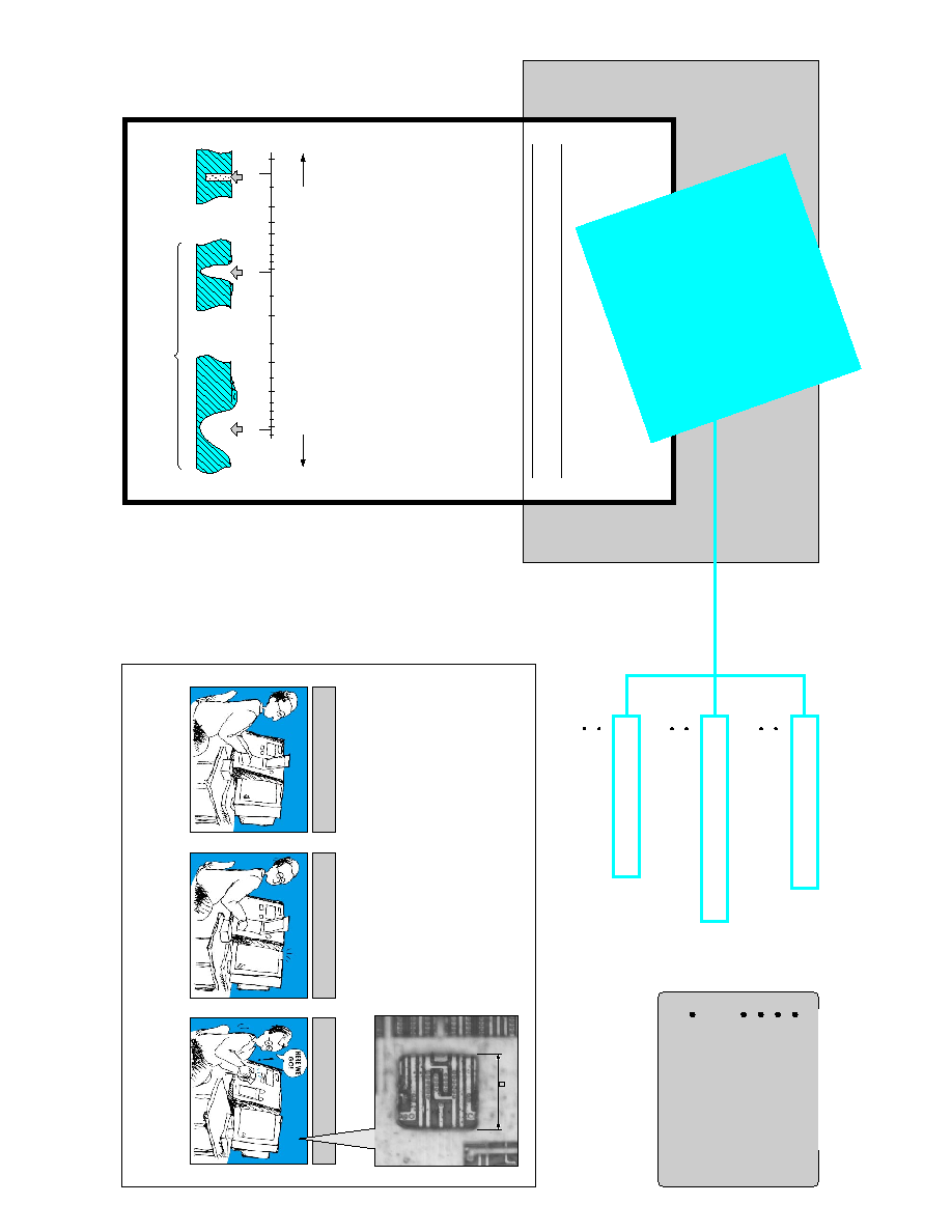
DUV laser beam
Insulation layer
Insulation layer
Silicon substrate
SiN passivation film
Aluminum pattern
Aluminum pattern
SiN passivation film
Aluminum pattern
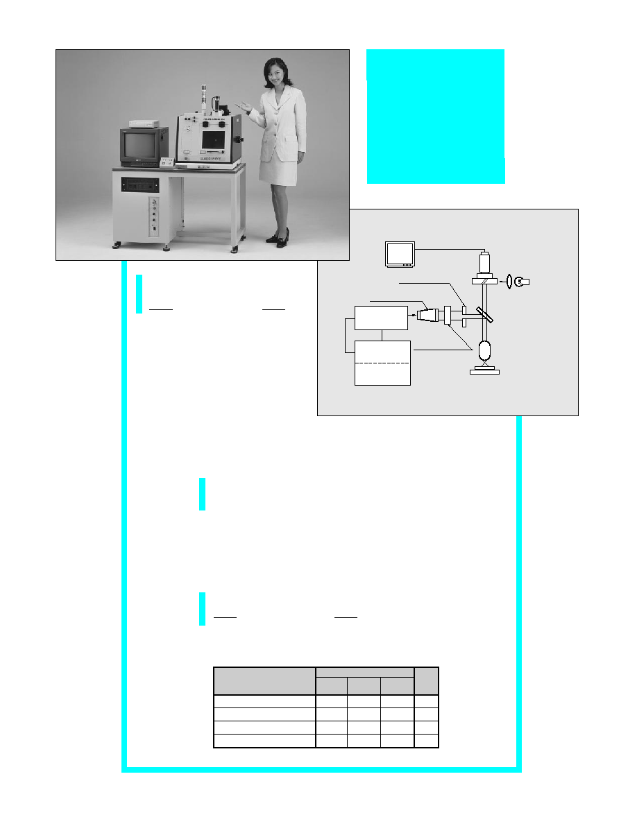
IC MICRO ABLATOR L7270
Allows selective removal of just the IC passivation film (polyimides, SiN, etc.)
and upper metallization layer (Al, etc.).
Strips away
aluminum pattern
Processing time of
just 10 seconds
Removes upper aluminum
layer in just seconds!
PATENT PENDING
30
µ
m
30
µ
m
DUV Laser
Application
10
3 minutes
10 seconds
2 minutes
Now just push the laser irradia-
tion button.
Check positioning on the moni-
tor.
Set the sample for processing.
Needs no special setup because
you use in an ordinary room
environment.
Simple &
easy in just
10 seconds!
PROCESSING SPEED
PROCESSING PRECISION
EASY PROCESSING
APPLICATIONS
Processing within 5 to 15 seconds
One-shot processing up to 30
◊
30
µ
m
EB tester hole drilling
Probing hole drilling
Pre-processing for FIB
Contour monitoring of
underlying metallization
pattern
Cutting of upper
aluminum pattern
Processing precision of 1
µ
m
Extremely fine processing with no thermal damage
Easy removal in an ordinary air atmosphere
Class 1 laser, without need for laser supervisor or
laser administration area
Processing
complete!
Allows selective removal of just the IC passivation film (polyimides,
SiN, etc.) and upper metal layer (Al, etc.).
IC MICRO
ABLATOR
L7270
DUV
*
Laser
processing means no
damage to other than
the target layer
The unique feature of DUV laser processing is that there is no thermal mechanism causing heat
melting or vaporization such as occurs in CO
2
lasers or IR-YAG lasers. DUV laser processing
instead provides a "no heat" ablation process allowing high precision processing without
carbonization or heat deformation.
Current lasers used for material processing and their schematic diagram
* DUV ..... Deep Ultraviolet
30
µ
m
30
µ
m
TLASC0021EA
200
400
600
1000
2000
Processing precision
(infrared)
Melting or vaporization
Melting or vaporization
Heat treating
(visible)
(ultraviolet)
bad
(nm)
CO
2
good
4000
6000
10000
IR-YAG
DUV
"No-heat"
ablation processing

Processing time: 10 seconds
Processing time: 10 seconds
Lets you
cutaway
without
damaging
adjacent
metallization
pattern!
Allows you to
monitor the
underlying
pattern
beneath thick
upper
metallization
layers!
When the
deadline for
the device
analysis
summary is fast
approaching!
Handy tool for shortening
failure analysis time
Drastic cut can now be made in processing time
for evaluation samples which up until now have
required a full day.
Time from sample setting, positioning through
to completion of processing is a mere 10
minutes*.
*Time may be sudject to change due to processing conditions.
Accurate
processing
toward
the deepest
metallization
pattern
Easy drilling
for EB tester
probing holes!
Processing time: 10 seconds
Enables
processing
jobs in normal
environment
How much more efficient would your work be if you could
take the colossal sums of time and money currently spent
on processing samples, and instead used that time and
money for evaluation and analysis?
Hamamatsu Photonics can now help you answer that
question thanks to development of an IC micro ablator.
Large area processing:
30
◊
30
µ
m in one shot
Now you can view the underlying metal pattern
hidden by the upper aluminum layer (power
supply or ground line), without impairing the
functions of this upper aluminum layer. Since
the circuit functions are still intact, you can
move to the next evaluation step right away
without having to change samples. One-shot
processing up to 30
◊
30
µ
m allows processing
a wide surface area in a short time.
Minimum processing
dimensions of 1
µ
m
Extremely fine processing to minimum
dimensions of 1
µ
m allows accurate cutting in
severely cramped metal patterns. For instance,
when evaluating a defective circuit, you can cut
interconnections between the upper aluminum
patterns to prevent adverse effects on other
circuits and then start checking for the defect.
High precision processing
with no heat deformation
The DUV laser directly cuts the molecular
bonds in non-heat processing. It makes
possible to remove alminum layer from 4thM
to 1stM one by one without giving any damage
to other layers.
Multiple holes in a short
time with ongoing
monitoring.
Simple and easy drilling for EB tester probing
holes is now a reality. Since drilling one hole
takes from only 2 to 10 seconds you can finish
drilling multiple holes in a short time. This
makes the L7270 a valuable support tool for
highly efficient evaluation and analysis.
Easy processing in normal
environments
All processing jobs on the L7270 can be easily
performed in a normal air environment in
contrast to FIB equipment which must be used
for processing in a vacuum.
2
µ
m
4
µ
m
SOLVED!
30
µ
m
30
µ
m
2
µ
m
4
µ
m
30
µ
m
30
µ
m
3
µ
m
3
µ
m
30
µ
m
30
µ
m
10
µ
m
10
µ
m
Time
L7270
Conventional
system
DUV laser beam
SiN passivation
film
Aluminum
pattern
SiN passivation
film
Aluminum
pattern
Aluminum pattern
Insulation layer
Silicon substate
Insulation layer
DUV laser beam
SiN passivation
film
Aluminum
pattern
SiN passivation
film
Aluminum
pattern
Aluminum pattern
Insulation layer
Silicon substate
Insulation layer
DUV laser beam
TLASF0091
IC MICR
O
ABLATOR
L727
0
DUV laser beam
SiN passivation
film
Polyimides
Polyimides
SiN passivation
film
Aluminum pattern
Silicon substate
Insulation layer
SiN passivation
film
Polyimides
Aluminum
pattern
Aluminum
pattern
Aluminum
pattern
Silicon substate
Insulation layer
Insulation
layer
Insulation
layer
SiN passivation
film
Polyimides
Aluminum
pattern
Aluminum
pattern
Insulation
layer
Enlarged viewing of the
processing status in real-time
Viewing optical system
The L7270 IC Micro Ablator removes a film in
the dry process so that processing status can be
monitored in real-time by use of an optical
microscope coupled to a 2/3-inch color CCD
camera. The image on the color monitor screen
is enlarged about 2000 times. By using an
optional 1/4-inch color CCD camera, the image
can be enlarged up to 7300 times (actual
magnification differs depending on combination
with the reduction projection lens).
All this allows the operator to work while
checking the processing status, position and
metal patterns.
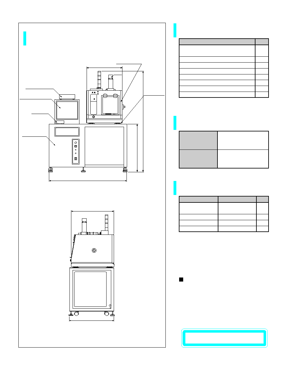
Versatile strokes of the processing stage
X-axis 76mm, Y-axis 30mm and Z-axis 30mm
The sample position and movement can be controlled by using the
manual X-Y stage.
The Z-axis stage aligns the laser beam to the sample according to
the sample thickness.
An computer-controlled automatic X-Y stage is available as an
option.
Adjustable processing dimensions
The light beam output from the DUV laser passes through a custom
optical system and is guided by a variable slit. This optical system
allows selecting the processing area according to the target pattern.
Optical projection system
Projection lens
◊
22
(option)
◊
80
(option)
◊
55
Parameter
Projection ratio
Lens working distance*
Minimum processing area
Maximum processing area
22: 1
24
2
80
◊
80
55: 1
8
1
30
◊
30
80: 1
2
0.5
15
◊
15
--
mm
µ
m
µ
m
Unit
* The distance from the projection lens to the sample surface.
TLASC0020EB
System Configuration
IC MICRO
ABLATOR
L7270
TLASF0089
COLOR MONITOR
CCD CAMERA
OPTICAL SYSTEM
ILLUMINATION
45
∞
REFLECTING MIRROR
HALOGEN LAMP
XYZ STAGE
PROJECTION LENS
BEAM
HOMOGENIZER
VARIABLE SLIT
ADJUSTABLE
ATTENUATOR
LASER
OSCILLATOR
CONTROLLER
POWER SUPPLY
Parameter
DIMENSIONS
(Unit: mm)
SYSTEM CONFIGURATION
TLASA0005EC
Main unit
(including laser, stage and optical systems)
2/3-inch color CCD camera
Remote switch
Low-magnification viewing objective
Vibration isolator
14-inch color monitor
Power cable: 5m
Electronic line generator
1
1
1
1
1
1
1
1
Qt.
GENERAL RATINGS
Input power voltage
Operating temperature
Operating humidity
Weight*
Single phase 100Vac/
6A Max. (50/60Hz)
+16 to +26
Below 60
Approx. 180
--
∞
C
%Rh
kg
Ratings
Unit
OPTIONS
Motorized X-Y stage
◊
22 projection lens
◊
80 projection lens
energy density monitor
1/4-inch color CCD camera
Processing system
Viewing system
Laser Product Safety Measures
The L7270 IC Micro Ablator conforms to the Japanese laser
safety regulations (JIS C 6802: radiation safety standards for
laser products) or equivalent international standards. In these
standards, lasers are classified into different classes to clarify
safety procedures for the manufacturer. These standards
define the safety measures and labeling to meet product safety
needs for each class. Please comply with the manufacturer's
safety measures and also with the appropriate laser safety
standards when using this device.
* Not including monitor and monitor stand
CLASS 1 LASER PRODUCT
VIEWING
COLOR MONITOR
REMOTE
SWITCH
POWER
SUPPLY UNIT
CAMERA
CONTROLLER
PROCESSING
UNIT
VIBRATION
ISOLATOR
CCD
500
610
1100
1420
630
695
FRONT VIEW
SIDE VIEW
Parameter