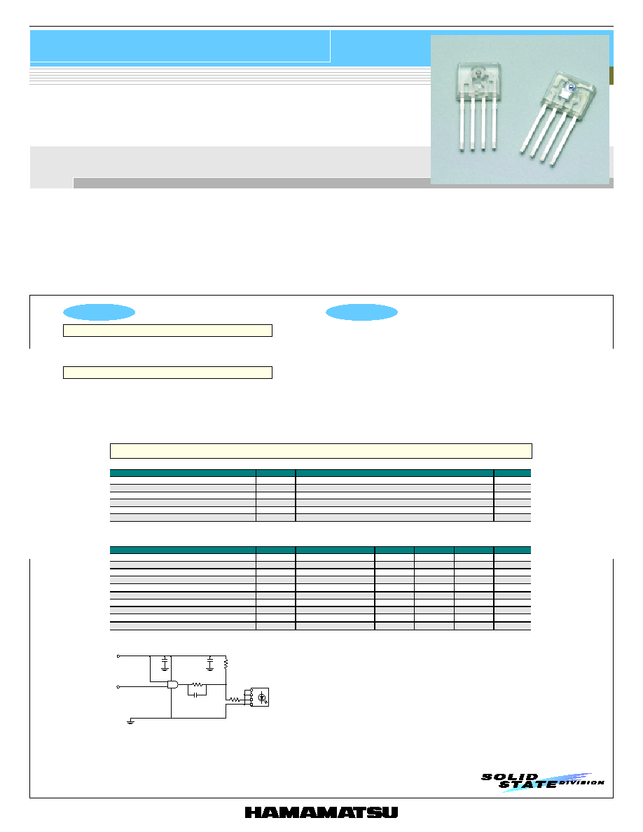
L8045 and S8046 are optical communication devices designed for POF (Plastic Optical Fiber) data links. L8045 is a highly
reliable, high-power LED that emits red light with a peak at 650 nm optimized for POF. A mini-lens is molded on the package for
efficient coupling to a POF. When used with our recommended driver circuit, a 50 Mbps transmitter can be configured at low cost.
S8046 is a high sensitivity, high-speed photo IC that receives signals at 50 Mbps and covers a wide dynamic range of 21.5 dB. The
output is TTL compatible. S8046 also features a standby mode in which operation automatically switches to low power dissipation
mode when no light is input and switches back to normal operation mode when light is input from the optical fiber. The internal IC
checks which mode is currently selected and this check signal is available from the mode output terminal. Current consumption in
standby mode is approximately 1/400th that of normal operation mode.
Features
Applications
L E D / P H O T O I C
Red LED/Photo IC for optical link
Emitter/receiver with standby mode suitable for 50 Mbps optical link
L8045/S8046
l High-speed data transmission even under poor environmental
conditions with high noise
l Peak wavelength: 650 nm
l High reliability
l High output
l Standby mode (low power dissipation)
l 4 to 50 Mbps
l Monolithic photo IC
l Optimum operation when used with L8045
l High reliability
l TTL output
l Wide dynamic range
L8045
S8046
I A bsolu te m axim um ratings (Ta= 25 ∞C )
P aram eter
S ym bol
Value
U nit
F orw ard current
I
.
40
m A
R everse voltage
V
4
5
V
P ow er dissipation *
1
P m ax
250
m W
O perating tem perature
Topr
-40 to +85
∞C
S torage tem perature
Tstg
-40 to +85
∞C
S oldering
-
230 ∞C, 5 s, at least 1.8 mm away from package surface
-
*1: D erate power dissipation at a rate of -1.75 m W /∞C above Ta= 25 ∞C
I E lectrica l and optica l characteristics (Ta=25 ∞C )
P aram eter
S ym bol
C ondition
M in.
Typ.
M ax.
U nit
D ata rate
fD
N R Z
D C
-
50
M bps
F orw ard voltage
V
.
I
.
=20 m A
-
1.9
2.3
V
R everse current
I
4
V
4
=5 V
-
-
10
µA
P eak wavelength
l p
I
.
=20 m A
-
650
-
nm
S pectral half width (FW H M )
D l
I
.
=20 m A
-
20
-
nm
F iber-coupled optical output
P o
*
2 , 3, 4
-13
-
-8
dBm
R ise tim e at pulse drive
tr
*
2 , 3, 4
20 to 80 %
-
-
8
ns
F all tim e at pulse drive
tf
*
2 , 3, 4
80 to 20 %
-
-
8
ns
P ulse distortion
D T
*
2 , 3, 4
-3
-
+1
ns
Jitter
D tj
*
2 , 3, 4
-
-
3
ns
*2: Input is a pseudo-random bi-phase signal at 50 M bps.
*3: M easu red w ith the recom m en ded driver c ircu it show n b elow. (M e asu rem ent cond itions: Vcc= 4.5 to 5.5 V, R 1= 360 W ,
R 2= 1.8 kW , R 3 =10 W , C 1 =56 pF )
*4: Average value (duty ratio 50 % ) m easured by using a plastic fiber of f1 m m . S I-P O F and N A =0.5 (G H 4001 m ade by
M itsubishi R ayon).
N ote)
1: A bypass capacitor (0.1 µF ) and another capacitor (4.7 µF ) are connected betw een Vcc and G N D at a position within 3 m m
from the lead.
2: The center of the optical fiber is aligned with the center of the lens on the package. The distance betw een the fiber end and
the lens is 0.1 m m .
L8045
Vcc
Icc
SIGNAL INPUT
1 14
2
7
74ACT08
3
4.7
mF
0.1
mF
R2
L8045
R1
C1
R3
1
2
3
4
KLEDC0018EB
1

HAMAMATSU PHOTONICS K.K., Solid State Division
1126-1 Ichino-cho, Hamamatsu City, 435-8558 Japan, Telephone: (81) 053-434-3311, Fax: (81) 053-434-5184, http://www.hamamatsu.com
U.S.A.: Hamamatsu Corporation: 360 Foothill Road, P.O.Box 6910, Bridgewater, N.J. 08807-0910, U.S.A., Telephone: (1) 908-231-0960, Fax: (1) 908-231-1218
Germany: Hamamatsu Photonics Deutschland GmbH: Arzbergerstr. 10, D-82211 Herrsching am Ammersee, Germany, Telephone: (49) 08152-3750, Fax: (49) 08152-2658
France: Hamamatsu Photonics France S.A.R.L.: 8, Rue du Saule Trapu, Parc du Moulin de Massy, 91882 Massy Cedex, France, Telephone: 33-(1) 69 53 71 00, Fax: 33-(1) 69 53 71 10
United Kingdom: Hamamatsu Photonics UK Limited: 2 Howard Court, 10 Tewin Road, Welwyn Garden City, Hertfordshire AL7 1BW, United Kingdom, Telephone: (44) 1707-294888, Fax: (44) 1707-325777
North Europe: Hamamatsu Photonics Norden AB: Smidesv‰gen 12, SE-171 41 Solna, Sweden, Telephone: (46) 8-509-031-00, Fax: (46) 8-509-031-01
Italy: Hamamatsu Photonics Italia S.R.L.: Strada della Moia, 1/E, 20020 Arese, (Milano), Italy, Telephone: (39) 02-935-81-733, Fax: (39) 02-935-81-741
Information furnished by HAMAMATSU is believed to be reliable. However, no responsibility is assumed for possible inaccuracies or omissions.
Specifications are subject to change without notice. No patent rights are granted to any of the circuits described herein. ©2002 Hamamatsu Photonics K.K.
Red LED/Photo IC for optical link
L8045/S8046
5.0
4.5 ± 0.3
(INCLUDING B
URR)
5.2 ± 0.3
(INCLUDING BURR)
0.5
1.27
(SPECIFIED AT THE LEAD OUT)
1.27
1.27
0.4
1.4
(2.15)
(1.5)
5.7 ± 0.4
4.3
(0.9)
10∞
10∞
5.0
Tolerance unless otherwise
noted: ±0.1, ±0.2∞
Shaded area indicates burr.
Values in parentheses indicate
reference value.
(0.9)
L8045
PIN No.
S8046
MODEOUT
GND
Vout
Vcc
CATHODE
CATHODE
ANODE
CATHODE
1.77
0.97
0.69
10∞
(0.9)
4.3
0.25
10∞
1.8
tso
NOT FIXED
NOT FIXED
OPTICAL INPUT
INPUT SIGNAL DATA
Vml
Vmh
Voh
Vol
NO INPUT SIGNAL
MODE OUTPUT
OUTPUT VOLTAGE
OUTPUT DATA
tos
I Mode switching chart (S8046)
KPICC0066EA
S8046
KPICA0042EA
I Dimensional outline (unit: mm)
Cat. No. KPIC1041E02
Aug. 2002 DN
I Absolute maximum ratings (Ta=25 ∞C)
Parameter
Symbol
Value
Unit
Supply voltage
Vcc
-0.5 to +7.0
V
Output voltage
Vo
-0.5 to Vcc+0.5
V
Output current
Io
10
mA
Power dissipation
P
250 *
5
mW
Operating temperature
Topr
-40 to +85
∞C
Storage temperature
Tstg
-40 to +85
∞C
Soldering
-
230 ∞C, 5 s, at least 1.8 mm away from package surface
-
*5: Derate power dissipation at a rate of -1.75 mW/∞C above Ta=25 ∞C
I Electrical and optical characteristics (Ta=25 ∞C, Vcc=4.5 to 5.5 V)
Parameter
Symbol
Condition
Min.
Typ
Max.
Unit
Data rate
fD
bi-phase signal
4
-
50
Mbps
Current consumption (in operation mode)
Icco
*
6, 7
-
-
40
mA
Current consumption (in standby mode)
Iccs
Pin= -•
-
-
100
µA
Minimum overload
Pimax
*
6, 7, 9, 10
-8
-
-
dBm
Minimum receiver input power
Pimin
*
6, 7, 9, 10
-
-
-29.5
dBm
H level output voltage
Voh
Ioh= -150 µA
*6, 7
2.7
-
-
V
L level output voltage
Vol
Iol=1.6 mA
*6, 7
-
-
0.4
V
Rise time
tr
-
-
5
ns
Output
voltage
Fall time
tf
0.4 to 2.7 V
*6, 7
-
-
5
ns
Pulse width distortion
Dt
*6, 7
-4
-
+8
ns
Jitter
Dtj
*6, 7
-
-
5
ns
Operation mode to standby mode switching input power
Psl
*6, 7, 9
-
-
-33
dBm
Standby mode to operation mode switching input power
Pop
*6, 7, 9
-
-
-30
dBm
Standby mode to operation mode switching time
tso
*
6
-
-
200
µs
Operation mode to standby mode switching time
tos
*
6
-
-
500
µs
H level voltage
Vmh
*
11
3.0
-
-
V
Mode
output
L level voltage
Vml
*
11
-
-
0.5
V
*6: Input is a pseudo-random bi-phase signal at 50 Mbps.
*7: C
L
=5 pF (including parasitic capacitance of probes, connectors and PC board)
*8: Optical input signal is generated by our standard signal generator.
*9: Average value (at 50 % duty ratio)
*10: Pe=10
-9
*11: H in standby mode, L in operation mode
Note)
3: A bypass capacitor (0.1 µF) and another capacitor (4.7 µF) are connected between Vcc and GND at a position within 3 mm
from the lead.
4: The center of the optical fiber is aligned with the center of the lens on the package. The distance between the fiber end and the
lens is 0.1 mm.
5: Output becomes undefined at a baud rate less than 4 Mbps.
2