Features
l
Photo IC output
l
Miniature package
Applications
l
Timing detection for copier, printer, etc.
l
Rotary encoder
l
Tape end detection for VTR, tape recorder, etc.
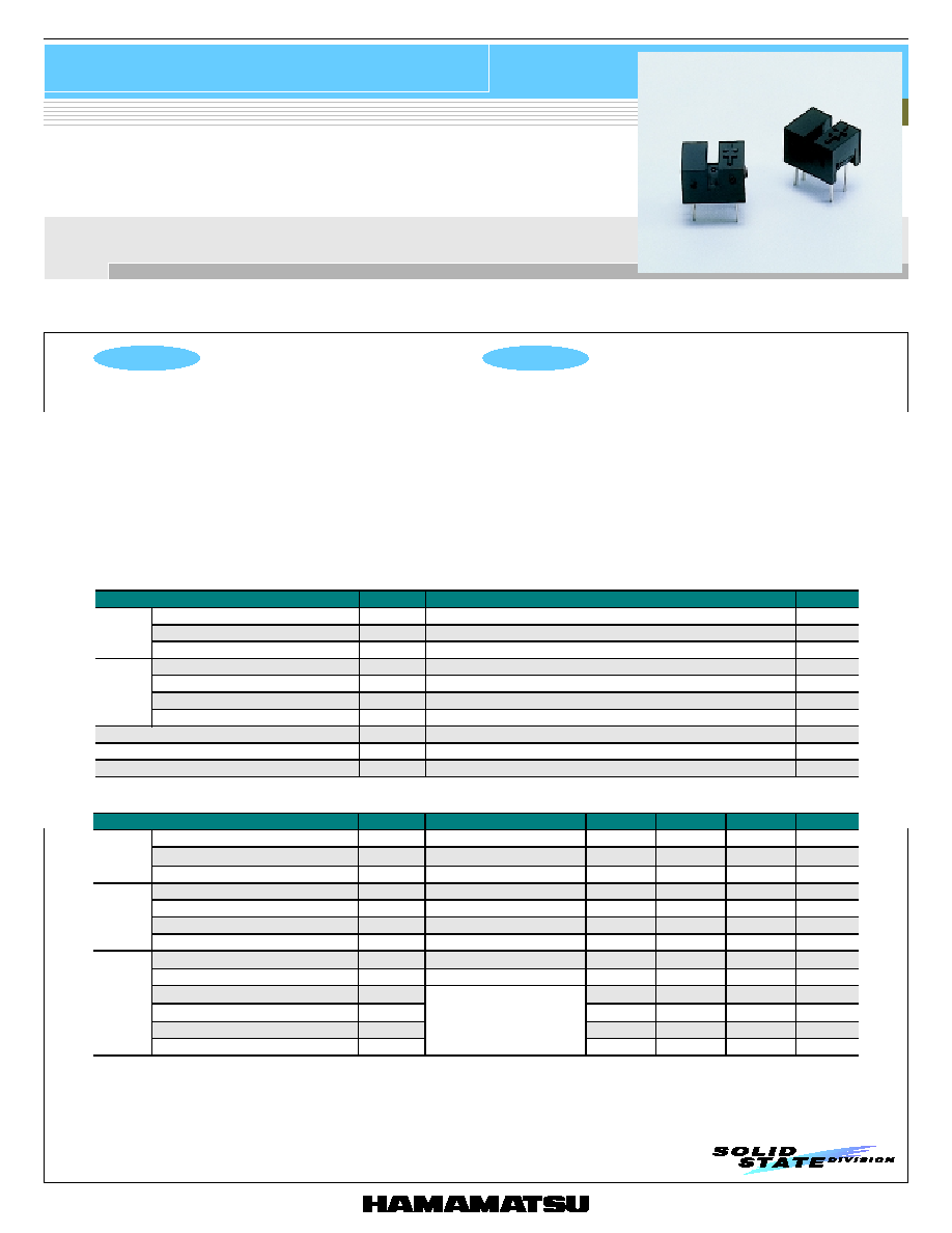
P H O T O I N T E R R U P T E R
Photointerrupter
Photo IC output
P6291
P6921 is a photointerrupter consisting of a high-power infrared LED and a photo IC. The photo IC incorporates a high-sensitivity photodiode, an
amplifier, a Schmitt trigger circuit and an output transistor, all integrated in a single chip. These elements are enclosed in a miniature C-shape
plastic package with a gap of 1.2 mm and a slit width of 0.2 mm, allowing object detection with high precision.
s Absolute maximum ratings (Ta=25
∞
C)
Parameter
Symbol
Value
Unit
Forward current
I
F
50
mA
Reverse voltage
V
R
5
V
Input
Power dissipation
P
80
mW
Supply voltage
Vcc
-0.5 to +7
V
Output voltage
Vo
-0.5 to +7
V
Output current
I
O
8
mA
Output
Power dissipation
Po
80
mW
Operating temperature
Topr
-25 to +85
∞C
Storage temperature
Tstg
-30 to +85
∞C
Soldering
-
260 ∞C, 3 s, at least 1 mm away from package surface
-
s Electrical and optical characteristics (Ta=25
∞
C, Vcc=5 V, unless otherwise noted)
Parameter
Symbol
Condition
Min.
Typ.
Max.
Unit
Forward voltage
V
F
I
F
=20 mA
-
1.25
1.45
V
Reverse current
I
R
V
R
=5 V
-
-
10
µA
Input
Terminal capacitance
Ct
V
R
=0 V, f=1 MHz
-
30
-
pF
Supply voltage
Vcc
2.2
-
7
V
Low level output voltage
V
OL
I
OL
=4 mA, I
F
=0 mA
-
0.1
0.4
V
High level output current
I
OH
Vo=5 V, I
F
=10 mA
-
-
10
µA
Output
Current consumption
I
CC
-
1.3
3.0
mA
L
H threshold input current
I
FLH
R
L
=1.2 k
-
0.6
6
mA
Hysterisis
-
I
FHL
/I
FLH
-
0.8
-
-
L
H propagation delay time
t
PLH
-
-
20
µs
H
L propagation delay time
t
PHL
-
-
30
µs
Rise time
tr
-
0.07
-
µs
Transfer
charac-
teristics
Fall time
tf
I
F
=10 mA
R
L
=1.2 k
-
0.03
-
µs
Note) Connect a capacitor of 0.01 µF or more between Vcc and GND.
1
Photointerrupter
P6291
HAMAMATSU PHOTONICS K.K., Solid State Division
1126-1 Ichino-cho, Hamamatsu City, 435-8558 Japan, Telephone: (81) 053-434-3311, Fax: (81) 053-434-5184, http://www.hamamatsu.com
U.S.A.: Hamamatsu Corporation: 360 Foothill Road, P.O.Box 6910, Bridgewater, N.J. 08807-0910, U.S.A., Telephone: (1) 908-231-0960, Fax: (1) 908-231-1218
Germany: Hamamatsu Photonics Deutschland GmbH: Arzbergerstr. 10, D-82211 Herrsching am Ammersee, Germany, Telephone: (49) 08152-3750, Fax: (49) 08152-2658
France: Hamamatsu Photonics France S.A.R.L.: 8, Rue du Saule Trapu, Parc du Moulin de Massy, 91882 Massy Cedex, France, Telephone: 33-(1) 69 53 71 00, Fax: 33-(1) 69 53 71 10
United Kingdom: Hamamatsu Photonics UK Limited: 2 Howard Court, 10 Tewin Road, Welwyn Garden City, Hertfordshire AL7 1BW, United Kingdom, Telephone: (44) 1707-294888, Fax: (44) 1707-325777
North Europe: Hamamatsu Photonics Norden AB: Smidesv‰gen 12, SE-171 41 Solna, Sweden, Telephone: (46) 8-509-031-00, Fax: (46) 8-509-031-01
Italy: Hamamatsu Photonics Italia S.R.L.: Strada della Moia, 1/E, 20020 Arese, (Milano), Italy, Telephone: (39) 02-935-81-733, Fax: (39) 02-935-81-741
Information furnished by HAMAMATSU is believed to be reliable. However, no responsibility is assumed for possible inaccuracies or omissions.
Specifications are subject to change without notice. No patent rights are granted to any of the circuits described herein. ©2003 Hamamatsu Photonics K.K.
Cat. No. KPC1007E03
Jul. 2003 DN
PULSE INPUT
I
F
5 V
Vo
GND
R
L
0.01 µF
I
F
t
PLH
Vo
tr
tf
V
OL
10 %
1.5 V
90 %
V
OH
50 %
t
PHL
KPCA0006EA
s
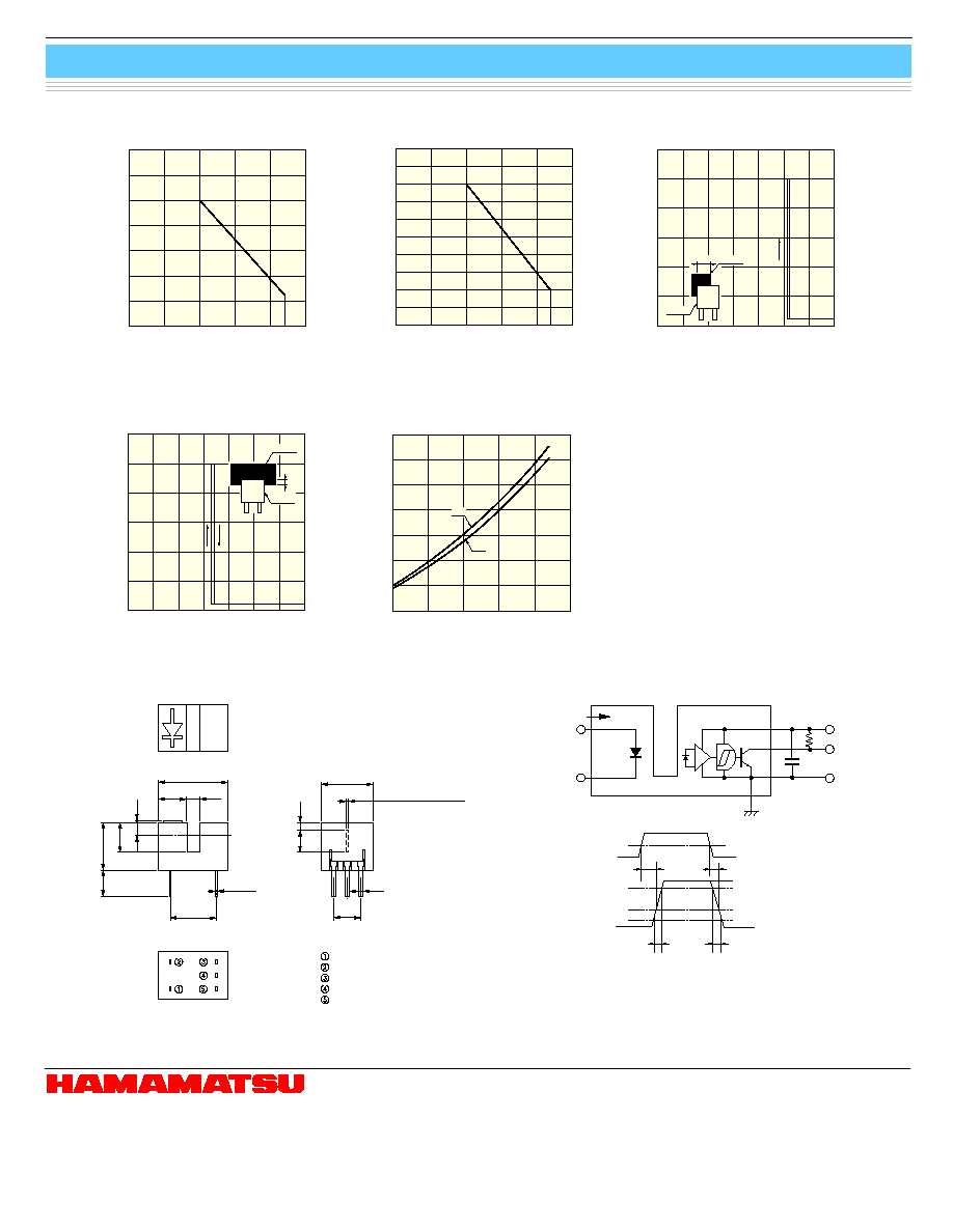
Dimensional outline (unit: mm)
s
LED forward current vs.
ambient temperature
s
Allowable power dissipation vs.
ambient temperature
s
Position detection characteristic (2)
s
Threshold current vs. ambient temperature
KPCC0007EB
s
Response time measuring circuit
KLEDB0081EA
KPCB0001EA
KPCB0005EA
KPCB0006EA
100
-25
0
25
50
75
0
AMBIENT TEMPERATURE (∞C)
FOR
W
ARD CURRENT (mA)
70
(Typ.)
60
50
40
30
20
10
POWER DISSIPATION (mW)
AMBIENT TEMPERATURE (∞C)
100
80
60
40
20
0
-25
0
25
50
75
100
(Typ.)
(Typ. Ta=25 ∞C, I
F
=5 mA, Vcc=5 V, R
L
=1.2 k
0
1
2
3
0
DISTANCE d (mm)
OUTPUT V
O
L
T
A
GE
(V)
1
2
3
4
5
6
MASK
d
P6291
(Typ. Ta=25 ∞C, Vcc=5 V, R
L
=1.2 k
)
-25
0
25
50
75
100
0.4
AMBIENT TEMPERATURE (∞C)
RELA
TIVE THRESHOLD
CURRENT
0.8
0.6
1
1.2
1.4
1.6
1.8
I
FLH
I
FHL
2.7
2.8
(1.2)
1.2
0.2
6.6
2.1
0.7
4.5
4.36
(SPECIFIED AT THE LEAD ROOT)
2.5 MIN.
4.9
0.2 (RECEIVER SIDE)
0.4
2.54
(SPECIFIED AT THE LEAD ROOT)
0.16
ANODE
CATHODE
Vcc
GND
V
O
EMITTER/
RECEIVER
AXIS
+0.2
-0.1
Tolerance unless otherwise noted: ±0.2
Values in parentheses are not guaranteed,
but for reference.
s
Position detection characteristic (1)
KPCB0004EB
(Typ. Ta=25 ∞C, I
F
=5 mA, Vcc=5 V, R
L
=1.2 k
)
0
1
2
3
0
DISTANCE d (mm)
OUTPUT V
O
L
T
A
GE
(V)
1
2
3
4
5
6
MASK
d
P6291
2