P6448 is a photoreflector consisting of a light modulation photo IC and an infrared LED, etc. The light modulation photo IC allows reliable
operation even under background disturbance light.
Features
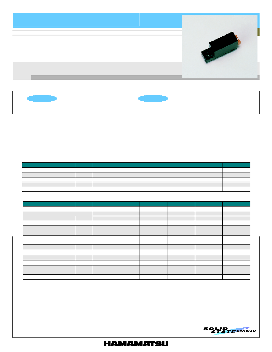
l Compact size (35 ◊ 10 ◊ 17 mm)
l Detection distance: 30 cm Typ.
l Allowable background light level: 2000 lx Min.
Applications
l Reflective optical switches
P H O T O R E F L E C T O R
Light modulation photoreflector
Compact module combining light modulation photo IC and infrared LED
P6448
s
Absolute maximum ratings (Ta=25 ∞C)
Parameter
Symbol
Value
Unit
Supply voltage
Vcc
-0.5 to +7
V
Output current
Io
50
mA
Output voltage
Vo
-0.5 to +12
V
Operating temperature
Topr
-20 to +60
∞C
Storage temperature
Tstg
-30 to +85
∞C
s
Electrical and optical characteristics (Ta=25 ∞C, Vcc=5 V, unless otherwise noted)
Parameter
Symbol
Condition
Min.
Typ.
Max.
Unit
Supply voltage
Vcc
4.75
-
5.25
V
Vo open, no emission
-
-
11
mA
Current consumption
Icc
During LED emission
-
80
200
mA
Low level output voltage
V
OL
I
OL
=16 mA
-
0.15
0.4
V
High level output voltage
V
OH
R
L
=4.7 k
(connected between Vcc-Vo)
4.5
-
-
V
Maximum detectable
distance *
1
d
Reflective paper with
reflectivity of 90 %
200
300
-
mm
Emission light pulse cycle
tc
-
130
-
µs
Emission light pulse width
tw
-
8
-
µs
HL Propagation delay time
t
PHL
-
-
1
ms
LH Propagation delay time
t
PLH
-
-
1
ms
Allowable background
light level
Ex
Background light: A
light source *
2
2000
-
-
lx
Hysteresis *
3
Hys
0.45
0.65
0.95
-
*1: Distance between P6448 and reflective paper (reflectivity 90 %) when the photo IC output level changes to L while bringing the
paper close to P6448 operated with H level output. (The photo IC has hysteresis characteristics, so the distance when the output
changes from L to H is longer than that when the output changes from H to L.)
*2: No direct light source within field of view.
*3: Hysteresis:
HL
LH
E
E
ELH: Input signal level at which the output changes from L to H level.
EHL: Input signal level at which the output changes from H to L level.

Light modulation photoreflector
P6448
HAMAMATSU PHOTONICS K.K., Solid State Division
1126-1 Ichino-cho, Hamamatsu City, 435-8558 Japan, Telephone: (81) 053-434-3311, Fax: (81) 053-434-5184, http://www.hamamatsu.com
U.S.A.: Hamamatsu Corporation: 360 Foothill Road, P.O.Box 6910, Bridgewater, N.J. 08807-0910, U.S.A., Telephone: (1) 908-231-0960, Fax: (1) 908-231-1218
Germany: Hamamatsu Photonics Deutschland GmbH: Arzbergerstr. 10, D-82211 Herrsching am Ammersee, Germany, Telephone: (49) 08152-3750, Fax: (49) 08152-2658
France: Hamamatsu Photonics France S.A.R.L.: 8, Rue du Saule Trapu, Parc du Moulin de Massy, 91882 Massy Cedex, France, Telephone: 33-(1) 69 53 71 00, Fax: 33-(1) 69 53 71 10
United Kingdom: Hamamatsu Photonics UK Limited: 2 Howard Court, 10 Tewin Road, Welwyn Garden City, Hertfordshire AL7 1BW, United Kingdom, Telephone: (44) 1707-294888, Fax: (44) 1707-325777
North Europe: Hamamatsu Photonics Norden AB: Smidesv‰gen 12, SE-171 41 Solna, Sweden, Telephone: (46) 8-509-031-00, Fax: (46) 8-509-031-01
Italy: Hamamatsu Photonics Italia S.R.L.: Strada della Moia, 1/E, 20020 Arese, (Milano), Italy, Telephone: (39) 02-935-81-733, Fax: (39) 02-935-81-741
Information furnished by HAMAMATSU is believed to be reliable. However, no responsibility is assumed for possible inaccuracies or omissions.
Specifications are subject to change without notice. No patent rights are granted to any of the circuits described herein. ©2001 Hamamatsu Photonics K.K.
Cat. No. KPC1002E01
Mar. 2001 DN
7.6 ± 0.5
(9)
(10.6)
5
10
CENTER OF
LIGHT EMISSION
CENTER OF
ACTIVE AREA
3.2
31.5 ± 0.5
23.5 ± 0.5
5
5.1
3.1 ± 0.5
4
4.5 ± 0.5
4
3.0
2
15 ± 0.5
Vcc
Vo
GND
Tolerance unless otherwise noted: ±0.2
Values in parentheses are not
guaranteed, but for reference.
s
Dimensional outline (unit: mm)
KPCA0001EA