 | –≠–ª–µ–∫—Ç—Ä–æ–Ω–Ω—ã–π –∫–æ–º–ø–æ–Ω–µ–Ω—Ç: R1307-01 | –°–∫–∞—á–∞—Ç—å:  PDF PDF  ZIP ZIP |

FEATURES
PHOTOMULTIPLIER TUBES
R1307, R1307-01
Information furnished by HA MAM ATS U is believed to be reliable. However, no responsibility is assumed for possible inaccuracies or omissions. Specifications are
subject to change without notice. No patent rights are granted to any of the circuits described herein.
©
1998 Hamamatsu Photonics K.K.
Subject to local technical requirements and regulations, availability of products included in this promotional material may var y. Please consult with our sales office.
For Scintillation Counting, Especially for Gamma Camera
76mm (3 Inch) Diameter, 8 Stage, Head-on Type
Bialkali Photocathode Photomultiplier Tubes
Quantum Efficiency at 420nm .................................................................................................................................... 30 -- %
Pulse Height Resolution
with
137
Cs Source (Note 1, 2) ........................................................................................................................... 6.3 7.0 %
with
57
Co Source (Note 1, 2) ............................................................................................................................ 8.5 9.0 %
Stability
Anode Current Drift (D.C. Output) (Note 1, 3) ............................................................................................................ 3 -- %
Long Term (MGD) (For 16 Hours at 1,000 cps) (Note 1, 4a) ...................................................................................... 0.5 -- %
Short Term (From 10,000 cps to 1,000 cps) (Note 1, 4b) ........................................................................................... 0.5 -- %
Typ. Max.
GENERAL
Parameter
Description/Value
Unit
Spectral Response
Wavelength of Maximum Response
Direct Interelectrode
Capacitances (approx.)
Window
Dynode
Operating Position
Weight (approx.)
Socket
nm
nm
pF
pF
--
--
µ
m
--
--
--
--
g
--
300 to 650
420
±
30
6.0
6.5
Borosilicate glass
1,500
±
0.001
Less than
±
50
Plano-plano
Box and grid
Alkali-antimonide
Any
190
E678-14A or equivalent
Anode to Dynode No. 8
Anode to All Other Electrodes
Material
Index of Refraction at 420nm
Face Plate Flatness
Shape
Structure
Material of Secondary Emitting Surface
MAXIMUM RATINGS (Absolute Maximum Values)
CHARACTERISTICS (at 25
∞
C)
Parameter
Min.
Unit
Parameter
Value
Unit
Supply Voltage
Average Anode Current (Note 5)
Average Cathode Current (Note 6)
Ambient Temperature
1500
300
0.1
50
-80 to +50 (R1307-01)
-30 to +50 (R1307)
Vdc
Vdc
mA
nA
∞
C
Between Anode and Cathode
Between Anode and Dynode No. 8
Anode Luminous Sensitivity (Note 1, 7)
Anode Blue Sensitivity (Note 1, 8)
Cathode Luminous Sensitivity (Note 9)
Cathode Blue Sensitivity (Note 10)
Gain
Anode Dark Current (Note 1, 11)
Time Response
Anode Pulse Rise Time (Note 1, 12)
Electron Transit Time (Note 1, 13)
3
--
80
10
--
--
--
--
30
3.2
110
12.0
2.7
◊
10
5
2
8
64
A/lm
A/lm-blue
µ
A/lm
µ
A/lm-blue
--
nA
ns
ns
--
--
--
--
--
20
--
--
Typ.
Max.
Figure 1: Typical Spectral Response
PHOTOMULTIPLIER TUBES R1307, R1307-01
TPMHB0520EA
Figure 2: Anode Sensitivity and Gain Characteristic
TPMHB0521EA
(Note 1, 7)
Figure 3: Typical Time Response (Note 1, 12, 13)
TPMHB0523EA
Figure 4: Typical Temperature Characteristic on
Dark Current (Note 1)
Measured after 15-hour storage in the dark
200
300
500
700
1000
1500
10
-3
10
-1
10
0
10
2
10
-4
SUPPLY VOLTAGE (V)
ANODE LUMINOUS SENSITIVITY (A/lm)
GAIN
10
-2
10
1
10
1
10
3
10
4
10
6
10
0
10
2
10
5
TYPICAL GAIN
TYPICAL ANODE SENSITIVITY
MINIMUM ANODE SENSITIVITY
100
10
1
0.1
0.01
200
400
600
800
1000
WAVELENGTH (nm)
CA
THODE RADIANT
SENSITIVITY
(mA/W)
QUANTUM EFFICIENCY
(%)
CATHODE
RADIANT
SENSITIVITY
QUANTUM
EFFICIENCY
500
1000
1500
2000
8
6
60
80
200
4
SUPPLY VOLTAGE (V)
TIME (ns)
40
20
10
100
TRANSIT TIME
RISE TIME
TPMHB0525EA
-60
-40
-20
0
+20
+40
0.1
10
100
10000
0.01
TEMPERATURE (
∞
C)
ANODE DARK CURRENT (nA)
1
1000
at 1500V
at 1000V
at 750V
NOTES
1: Voltage distribution ratio
Supply voltage (Ebb) = 1000Vdc
K: cathode, G: Focusing Electrode, Dy: Dynode, P: Anode
2.
Scintillator is manufactured by Harshaw Chemical, (Type 12A12), and
BICRON (Type 3R3), Nal (Tl), 3" diameter 3" thickness.
3.
Drift for 1 hour after 10 minutes of initial warming up with 10
µ
A anode
current.
4.
A
137
Cs source and an Nal (Tl) crystal are employed to measure the
pulse height. Warming up time is about 1 hour.
a) Long term (Mean Gain Deviation) is defined as follows.
where P is the mean pulse height averaged over n readings, P
i
is the
pulse height at the i-th reading, and n is the total number of readings.
b) Short term
Scintillator (Nal (Tl) crystal) is 3" diameter 3" thickness. The photomul-
tiplier is first operated at about 10,000 cps. The photopeak counting
is then decreased to approximately 1,000 cps by increasing the dis-
tance between source and crystal on the tube.
5. Averaged over any interval of 30 seconds maximum.
6. Same as Note 5 and the whole photocathode is illuminated.
7.
The light source is a tungsten filament lamp operated at a distribution
temperature of 2856K. The light input of 10
-7
lumen is used.
8.
The value is anode output current when the blue filter (Corning CS 5-58
polished to 1/2 stock thickness) is interposed between the light source
(providing 10
-7
lumen) and the tube under the same condition as Note 7.
9.
The condition is the same shown in Note 7 except that the value of light
input is 10
-4
limen and 150 volts are applied between cathode and all oth-
er electrodes connected together as anode.
10. These values are cathode output current when the blue filter (Corning
CS 5-58 polished to 1/2 stock thickness) is interposed between the light
source (providing 10
-4
lumen) and the tube under the same condition as
Note 9.
11. Measured after 5-second strage in the dark.
12. The rise time is the time for the output pulse to rise from 10% to 90% of
the peak output when the tube is illuminated by a flash of light of very
short duration. In measurement, the whole photocathode is illuminated.
13. The electron transit time is the interval between the arrival of delta func-
tion light pulse at the entrance window of the tube and the time when the
output pulse at the anode terminal reaches peak amplitude.
14. m is the mean value of total counts, i.e.
Test conditions: Incident light wavelength is 400nm. Supply voltage is
+1300V. Ambient temperature is 20
∞
C.
Electrodes
Distribution
Ratio
K
Dy1
G
1
Dy2
1
Dy3
1
Dy4
1
Dy5
1
Dy6
1
Dy7
1
Dy8
1
1
1
P
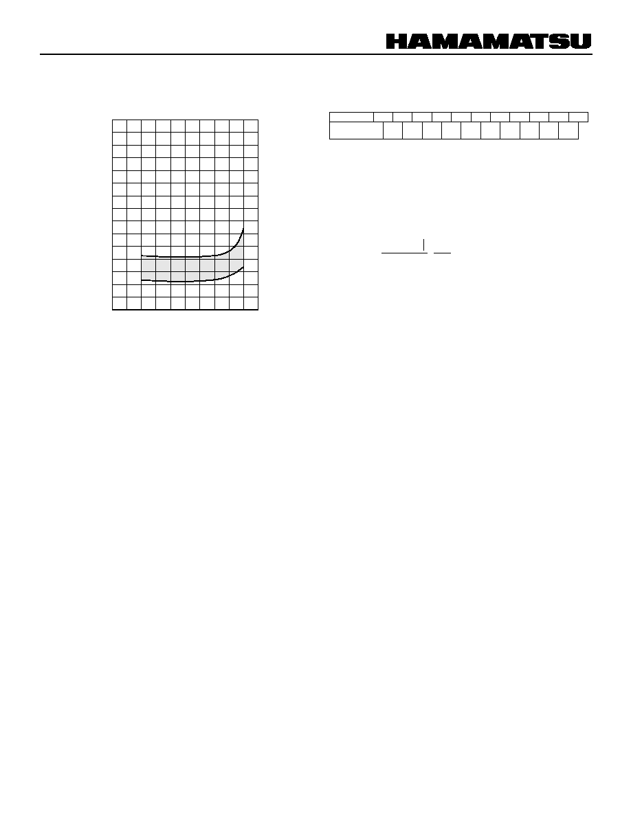
Figure 5: Typical Temperature Coefficient of Anode
Sensitivity (-20 to +60
∞
C, Note 1)
TPMHB0527EA
200
300
400
500
600
700
0
-1.0
+2.0
WAVELENGTH (nm)
TEMPERATURE COEFFICIENT (%/
∞
C)
+1.0
Dg = . (%)
n
i
= 1
P - P
i
100
P
n
(counts per channel) =
(counts per channel)
m
0.3m
3m
m

Figure 6: Dimensional Outlines (Unit: mm)
TPMH1214E01
AUG. 1998
HAMAMATSU PHOTONICS K.K., Electoron Tube Center
314-5, Shimokanzo, Toyooka-village, Iwata-gun, Shizuoka-ken, 438-0193, Japan, Telephone: (81)539/62-5248, Fax: (81)539/62-2205
U.S.A.: Hamamatsu Corporation: 360 Foothill Road, P. O. Box 6910, Bridgewater. N.J. 08807-0910, U.S.A., Telephone: (1)908-231-0960, Fax: (1)908-231-1218
Germany: Hamamatsu Photonics Deutschland GmbH: Arzbergerstr. 10, D-82211 Herrsching am Ammersee, Germany, Telephone: (49)8152-375-0, Fax: (49)8152-2658
France: Hamamatsu Photonics France S.A.R.L.: 8, Rue du Saule Trapu, Parc du Moulin de Massy, 91882 Massy Cedex, France, Telephone: (33)1 69 53 71 00, Fax: (33)1 69 53 71 10
United Kingdom: Hamamatsu Photonics UK Limited: Lough Point, 2 Gladbeck Way, Windmill Hill, Enfield, Middlesex EN2 7JA, United Kingdom, Telephone: (44)181-367-3560, Fax: (44)181-367-6384
North Europe: Hamamatsu Photonics Norden AB: F‰rˆgatan 7, S-164-40 Kista Sweden, Telephone: (46)8-703-29-50, Fax: (46)8-750-58-95
Italy: Hamamatsu Photonics Italia: S.R.L.: Strada della Moia, 1/E, 20020 Arese, (Milano), Italy, Telephone: (39)02-935 81 733, Fax: (39)02-935 81 741
TACCA0044EB
TPMHA0433EA
TPMHA0078EA
PHOTOMULTIPLIER TUBES R1307, R1307-01
Warning - Personal Safety Hazards
Electrical Shock -- Operating voltage
applied to this device presents shock hazard.
19.8
11
56
62
30
17
2
1
2
3
4
5
6
7
8
9
10
11
12
13
14
DY1
DY2
IC
DY4
DY5
DY6
DY7
DY8
IC
IC
P
DY3
G
K
76.0
±
0.8
70MIN.
127
±
3
150MAX.
56.5
±
0.5
51.5
±
1.5
FACEPLATE
PHOTO-
CATHODE
14 PIN BASE
JEDEC
No. B14-38
1
2
5
6
7
8
9 10
11
12
13
17
18
DY1
DY2
DY4
DY5
DY6
DY7
DY8
NC
NC
P
DY3
G
K
76.0
±
0.8
70MIN.
110
±
1.5
68MIN.
13MAX.
56.5
±
0.5
51.5
±
1.5
FACEPLATE
PHOTO-
CATHODE
1.0
SEMIFLEXIBLE
LEADS
Basing Diagram
(Bottom View at Semiflexible Leads)
*Basing diagram of temporary
base is the same as that of R1307.
R1307
R1307-01
Socket (OPTION)
(E678-14A)