 | –≠–ª–µ–∫—Ç—Ä–æ–Ω–Ω—ã–π –∫–æ–º–ø–æ–Ω–µ–Ω—Ç: R1477-06 | –°–∫–∞—á–∞—Ç—å:  PDF PDF  ZIP ZIP |
GENERAL
FEATURES
Parameter
Description/Value Unit
Spectral Response
Wavelength of Maximum Response
Photocathode
Window Material
Dynode
Direct
Interelectrode
Capacitances
Base
Weight
Suitable Socket
Suitable Socket Assembly
nm
nm
--
mm
--
--
--
--
pF
pF
--
g
--
--
185 to 900
450
Multialkali
8
◊
24
UV glass
Multialkali
Circular-cage
9
Approx. 4
Approx. 6
11-pin base
JEDEC No. B11-88
Approx. 45
E678-11A (Option)
E717-21 (Option)
Material
Minimum Effective Area
Secondary Emitting Surface
Structure
Number of Stages
Anode to Last Dynode
Anode to All Other Electrodes
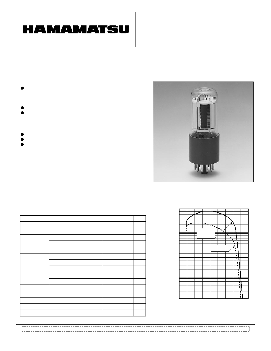
PHOTOMULTIPLIER TUBE
R1477-06
High Sensitivity Multialkali Photocathode (185 nm to 900 nm)
28 mm (1-1/8 Inch) Diameter, 9-stage, Side-On
Figure 1: Typical Spectral Response
TPMSB0182EA
The R1477-06 has a high sensitivity multialkali photocathode (even
higher than the R928). The spectral response covers a wide range
from 185 to 900 nm with a peak response at approximately 450 nm.
The R1477-06 also features the combination of high gain and low dark
current.
The R1477-06 is recommended for use in spectrophotometry and oth-
er low light level applications requiring super-high cathode sensitivity
from the UV to the near IR regions of the spectrum.
High Cathode Sensitivity
Radiant at 450nm ........................................................... 80 mA/W
Luminous ...................................................................... 375
µ
A/lm
Quantum Efficiency at 370 nm ............................................. 24 %
Wide Spectral Response ......................................... 185 to 900 nm
Low Anode Dark Current ........................................ 3 nA at 1000 V
(after 30 minute storage)
APPLICATIONS
UV to IR Spectrophotometers
Laser Detection Systems
Pollution Monitors
Information furnished by HAMAMATSU is believed to be reliable. However, no responsibility is assumed for possible inaccuracies or omissions. Specifications are
subject to change without notice. No patent rights are granted to any of the circuits described herein. ©1999 Hamamatsu Photonics K.K
Subject to local technical requirements and regulations, availability of products included in this promotional material may vary. Please consult with our sales office.
100
10
1
0.1
0.01
200
500
700
900
400
100
300
600
800
1000
WAVELENGTH (nm)
CA
THODE RADIANT
SENSITIVITY
(mA/W)
QUANTUM EFFICIENCY
(%)
QUANTUM
EFFICIENCY
CATHODE
RADIANT
SENSITIVITY

MAXIMUM RATINGS (Absolute Maximum Values at 25
∞
C)
Parameter
Value
Unit
Supply Voltage
Average Anode Current
A
Ambient Temperature
Vdc
Vdc
mA
∞
C
1250
250
0.1
-80 to +50
Between Anode and Cathode
Between Anode and Last Dynode
PHOTOMULTIPLIER TUBE R1477-06
CHARACTERISTICS (at 25
∞
C)
Table 1: Voltage Distribution Ratio
Parameter
Min.
Unit
Cathode
Sensitivity
Anode
Sensitivity
Gain
E
Anode Dark Current
F
(After 30 minute storage in the darkness)
ENI (Equivalent Noise Input)
G
Time
Response
E
Anode Current
Stability
L
µ
A/lm
mA/W
mA/W
mA/W
mA/W
%
--
µ
A/lm-b
A/lm
A/W
A/W
A/W
A/W
--
nA
W
ns
ns
ns
%
%
350
--
--
--
--
--
0.25
--
1000
--
--
--
--
--
--
--
--
--
--
--
--
Max.
--
--
--
--
--
--
--
--
--
--
--
--
--
--
50
--
--
--
--
--
--
Typ.
375
40
80
62
5.0
24
0.35
1.0
2000
2.4
◊
10
5
4.2
◊
10
5
3.3
◊
10
5
2.7
◊
10
4
5.3
◊
10
6
3
1.7
◊
10
-16
2.2
22
1.2
0.1
1
Luminous
B
Radiant
Quantum
Efficiency
Red/White Ratio
C
Blue
D
Luminous
E
Radiant
Anode Pulse Rise Time
H
Electron Transit Time
J
Transit Time Spread (TTS)
K
Current Hysteresis
Voltage Hysteresis
at 254 nm
at 450 nm
at 633 nm
at 852 nm
at 370 nm
at 254nm
at 450nm
at 633nm
at 852nm
NOTES
A: Averaged over any interval of 30 seconds maximum.
B: The light source is a tungsten filament lamp operated at
a distribution temperature of 2856K. Supply voltage is
100 volts between the cathode and all other electrodes
connected together as anode.
C: Red/white ratio is the quotient of the cathode current
measured using a red filter (Toshiba R-68) interposed
between the light source and the tube by the cathode
current measured with the filter removed under the
same conditions as Note B.
D: The value is cathode output current when a blue filter
(Corning CS 5-58 polished to 1/2 stock thickness) is
interposed between the light source and the tube under
the same conditions as Note B.
E: Measured with the same light source as Note B and with
the voltage distribution ratio shown in Table 1 below.
F: Measured with the same supply voltage and voltage dis-
tribution ratio as Note E after removal of light.
G: ENI is an indication of the photon-limited signal-to-noise
ratio. It refers to the amount of light in watts to produce
a signal-to-noise ratio of unity in the output of a
photomultiplier tube.
where q = Electronic charge (1.60
◊
10
-19
coulomb)
ldb = Anode dark current (after 30 minute storage)
in amperes
G = Gain
f = Bandwidth of the system in hertz. 1 hertz is
used.
S = Anode radiant sensitivity in amperes per watt
at the wavelength of peak response.
H: The rise time is the time for the output pulse to rise from
10% to 90% of the peak amplitude when the entire pho-
tocathode is illuminated by a delta function light pulse.
J: The electron transit time is the interval between the
arrival of delta function light pulse at the entrance
window of the tube and the time when the anode output
reaches the peak amplitude. In measurement, the
whole photocathode is illuminated.
K. Also called transit time jitter. This is the fluctuation in
electron transit time between individual pulses in the
signal photoelectron mode, and may be defined as the
FWHM of the frequency distribution of electron transit
times.
L. Hysteresis is temporary instability in anode current after
light and voltage are applied.
(1) Current Hysteresis
The tube is operated at 750 volts with an anode current of 1
micro-ampere for 5 minutes. The light is then removed from
the tube for a minute. The tube is then re-illuminated by the
previous light level for a minute to measure the variation.
(2)Voltage Hysteresis
The tube is operated at 300 volts with an anode current of
0.1 micro-ampere for 5 minutes. The light is then removed
from the tube and the supply voltage is quickly increased to
800 volts. After a minute, the supply voltage is reduced to
the previous value and the tube is re-illuminated for a
minute to measure the variation.
Supply Voltage= 1000Vdc
K: Cathode, Dy: Dynode, P: Anode
Electrodes
Distribution
Ratio
K
Dy1
1
Dy2
1
Dy3
1
Dy4
1
Dy5
1
Dy6
1
Dy7
1
Dy8
1
Dy9
1
1
P
ENI =
2q∑ldb∑G∑
f
S
Hysteresis =
◊
100 (%)
Imax. - Imin.
Ii
Imin.
Ii
Imax.
ANODE
CURRENT
0
5
6
7
(MINUTES)
TIME

Figure 2: Anode Luminous Sensitivity and Gain
TPMSB0183EA
TPMSB0184EA
Figure 3: Typical Time Response
Figure 4: Typical Temperature Coefficient of Anode
Sensitivity
TPMSB0185EA
TPMSB0186EA
Figure 5: Typical Temperature Characteristic of Dark
Current (at 1000V, after 30 minute storage)
10
4
10
3
10
2
10
1
10
0
10
-1
10
-2
10
8
10
7
10
6
10
5
10
4
10
3
10
2
200
300
500
700
1000
1500
SUPPLY VOLTAGE (V)
ANODE LUMINOUS SENSITIVITY
(A/lm)
GAIN
TYPICAL
ANODE
SENSITIVITY
MINIMUM ANODE
SENSITIVITY
TYPICAL
GAIN
200
100
80
60
40
20
10
8
6
4
2
1
300
500
700
1000
1500
SUPPLY VOLTAGE (V)
TIME (ns)
TRANSIT
TIME
RISE TIME
+1.2
+0.8
+0.4
0
-0.4
-0.8
-1.2
200
400
600
800
1000
WAVELENGTH (nm)
TEMPERA
TURE COEFFICIENT
(%/
∞
C)
100
10
1
0.1
0.01
-40
-20
0
+20
+40
TEMPERATURE (
∞
C)
ANODE DARK CURRENT
(nA)
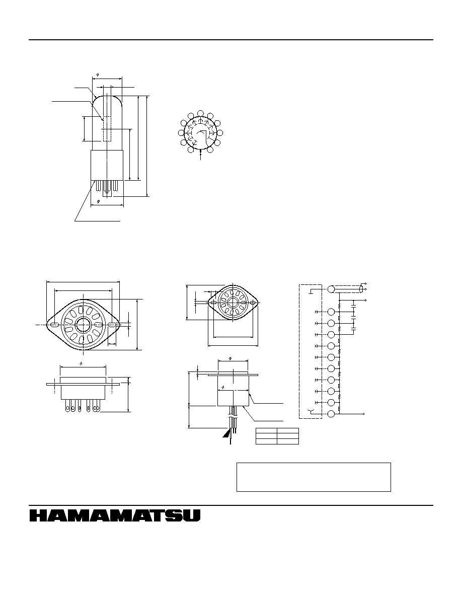
Figure 6: Dimensional Outline and Basing Diagram (Unit: mm)
TPMS1066E01
FEB. 1999
TPMSA0008EA
TACCA0064EA
TACCA0002EE
Figure 7: Optional Accessories (Unit: mm)
E678-11A (Socket)
D Type Socket Assembly E717-21
PHOTOMULTIPLIER TUBE R1477-06
Warning-Personal Safety Hazards
Electrical Shock Operating voltage
applied to this device presents shock hazard.
* Hamamatsu also provides C4900 series modular type high voltage power
supplies and C6270 series DP type socket assemblies which incorporate
a DC to DC converter type high voltage power supply.
HAMAMATSU PHOTONICS K.K., Electron Tube Center
314-5, Shimokanzo, Toyooka-village, Iwata-gun, Shizuoka-ken, 438-0193, Japan, Telephone: (81)539/62-5248, Fax: (81)539/62-2205
U.S.A.: Hamamatsu Corporation: 360 Foothill Road, P. O. Box 6910, Bridgewater. N.J. 08807-0910, U.S.A., Telephone: (1)908-231-0960, Fax: (1)908-231-1218
Germany: Hamamatsu Photonics Deutschland GmbH: Arzbergerstr. 10, D-82211 Herrsching am Ammersee, Germany, Telephone: (49)8152-375-0, Fax: (49)8152-2658
France: Hamamatsu Photonics France S.A.R.L.: 8, Rue du Saule Trapu, Parc du Moulin de Massy, 91882 Massy Cedex, France, Telephone: (33)1 69 53 71 00, Fax: (33)1 69 53 71 10
United Kingdom: Hamamatsu Photonics UK Limited: Lough Point, 2 Gladbeck Way, Windmill Hill, Enfield, Middlesex EN2 7JA, United Kingdom, Telephone: (44)181-367-3560, Fax: (44)181-367-6384
North Europe: Hamamatsu Photonics Norden AB: Smidesv gen 12, SE-171-41 SOLNA, Sweden, Telephone: (46)8-509-031-00, Fax: (46)8-509-031-01
Italy: Hamamatsu Photonics Italia: S.R.L.: Strada della Moia, 1/E, 20020 Arese, (Milano), Italy, Telephone: (39)02-935 81 733, Fax: (39)02-935 81 741
33
5
49
3.5
38
29
4
18
1
2
4
3
5
7
6
8
9
10
K
DY1
DY2
DY3
DY4
DY5
DY6
DY7
DY8
DY9
P
DIRECTION OF LIGHT
Basing Diagram
(Bottom View)
28.5≠1.5
8MIN.
T9
BULB
PHOTOCATHODE
24MIN.
49.0≠2.5
80MAX.
94MAX.
32.2≠0.5
11 PIN BASE
JEDEC No. B11-88
11
POTTING
COMPOUND
R to R10
C1 to C3
: 330k
: 0.01
µ
F
3.5
33.0 ≠ 0.3
49.0 ≠ 0.3
29
38.0 ≠ 0.3
4
L
450 ≠ 10
5
31.0 ≠ 0.5
HOUSING
(INSULATOR)
Type No.
E717-21
E717-63
L
41 ≠ 0.5
30 ≠ 0.5
R10
R9
R8
R7
R6
R5
R4
R3
R2
R1
DY9
DY8
DY7
DY6
DY5
DY4
DY3
DY2
DY1
C3
C2
C1
SIGNAL GND
SIGNAL OUTPUT
RG-174/U (BLACK)
-HV
AWG22 (VIOLET)
P
K
10
POWER SUPPLY GND
AWG22 (BLACK)
SOCKET
PIN No.
PMT
9
8
7
6
5
4
3
2
1
11