 | –≠–ª–µ–∫—Ç—Ä–æ–Ω–Ω—ã–π –∫–æ–º–ø–æ–Ω–µ–Ω—Ç: R4220 | –°–∫–∞—á–∞—Ç—å:  PDF PDF  ZIP ZIP |

Very High Cathode Sensitivity with Low Noise Photocathode
GENERAL
FEATURES
Parameter
Description/Value Unit
Spectral Response
Hamamatsu R4220 features extremely high cathode sen-
sitivity, high Gain, and low dark current.
Variant tube (R4220P) specially selected for photon
counting application is also available.
The R4220 is useful for fluorescence, chemilumines-
cence, Raman spectroscopy and low light level detec-
tion.
Wavelength of Maximum Response
185 to 710
nm
nm
Photocathode
MateriaI
410
Structure
4
pF
Anode to Last Dynode
6
pF
Anode to All Other Electrodes
Minimum Effective Area
Low noise bialkali
Secondary Emitting Surface
Low noise bialkali
mm
Window Material
Weight
8 24
g
45
Dynode
Direct Interelectrode Capacitances
Base
SuitabIe Socket Assembly
UV glass
Circular-cage
Number of Stages
9
11-pin base
JEDEC No. B11-88
E717≠21 (option)
SuitabIe Socket
E678≠11A (option)
lnformation furnished by HA MAM ATS U is believed to be reliabIe. However, no responsibility is assumed for possibIe inaccuracies or ommissions. Specifications are
subject to change without notice. No patent right are granted to any of the circuits described herein.
©
1994 Hamamatsu Photonics K.K.
Subject to local technical requirements and regulations, availability of products included in this promotional material may var y. Please consult with our sales office.
R4220P(For Photon Counting)
PHOTOMULTlPLlER TUBES
R4220
Spectral Response ...................................
High Cathode Sensitivity
Luminous ......................................................
Radiant at 410nm ............................................
High Anode Sensitivity (at 1000V)
Low Dark Current ....................................................
Luminous .......................................................
Radiant at 410nm .....................................
185 to 710 nm
0.2nA
Low Dark Counts (R4220P) ................................... 10 cps
100 A/lm
70 mA/W
1200A/lm
8.4 10
5
A/W
Figure 1: Typical Spectral Response
100
10
1
0.1
0.01
100
200
300
400
500
600
700
800
WAVELENGTH (nm)
CATHODE RADIANT SENSITIVITY (mA/W)
QUANTUM EFFICIENCY (%)
QUANTUM
EFFICIENCY
CATHODE
RADIANT
SENSITIVITY
TPMSB0010EA
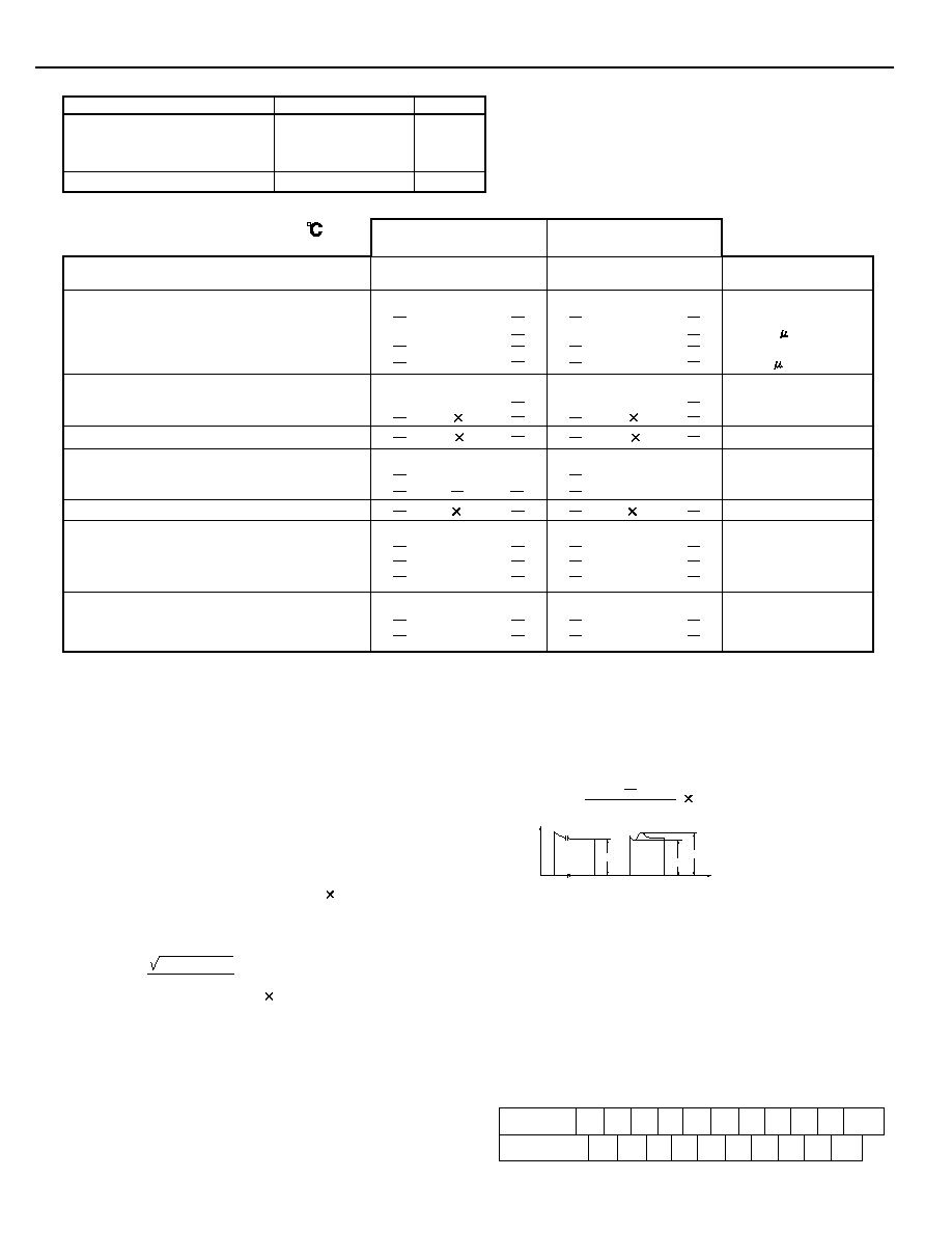
MAXIMUM RATINGS (Absolute Maximum Values)
Parameter
Value
Supply Voltage
Between Anode and Cathode
Between Anode and Last Dynode
1250
250
0.1
Vdc
Vdc
mA
Average Anode Current
A
Unit
CHARACTERISTlCS (at 25 )
NOTES
Parameter
Min.
Typ.
Typ.
Max.
R4220
for General Purpose
R4220P
for Photon Counting
Cathode Sensitivity
Anode Dark Current
F
Anode Dark Counts
F
Anode Sensitivity
After 30minutes Storage in the darkness
0.2
2.0
Anode Current Stability
L
A:
B:
C:
D:
E:
F:
G:
H:
J:
Averaged over any interval of 30 seconds maximum.
The light source is a tungsten filament lamp operated at a distribution tem-
perature of 2856K. Supply voltage is 150 volts between the cathode and all
other electrodes connected together as anode.
The value is cathode output current when a blue filter(Corning CS-5-58
polished to 1/2 stock thickness) is interposed between the light source and
the tube under the same condition as Note B.
Measured with the same light source as Note B and with the anode-to-
cathode supply voltage and voltage distribution ratio shown in Table 1 be-
low.
Measured with the same supply voltage and voltage distribution ratio as
Note D after removal of light.
Measured at the voltage producing the gain of 1 10
6
.
ENI is an indication of the photon-limited signal-to-noise ratio. It refers to
the amount of light in watts to produce a signal-to-noise ratio of unity in the
output of a photomultiplier tube.
where q = Electronic charge (1.60 10
-19
coulomb).
ldb = Anode dark current(after 30 minute storage) in amperes.
G = Gain.
f = Bandwidth of the system in hertz. 1 hertz is used.
S = Anode radiant sensitivity in amperes per watt at the wave-
length of peak response.
The rise time is the time for the output pulse to rise from 10% to 90% of the
peak amplitude when the entire photocathode is illuminated by a delta
function light pulse.
The electron transit time is the interval between the arrival of delta function
light pulse at the entrance window of the tube and the time when the anode
output reaches the peak amplitude. In measurement, the whole photo-
cathode is illuminated.
K:
L:
Also called transit time jitter. This is the fluctuation in electron transit time
between individual pulses in the signal photoelectron mode, and may be
defined as the FWHM of the frequency distribution of electron transit times.
Hysteresis is temporary instability in anode current after light and voltage
are applied.
ENI =
S
2q.ldb.G. f
Current Hysteresis
Voltage Hysteresis
0.1
1.0
Radiant at 410nm (Peak)
70
Blue
C
8
Anode Pulse Rise Time
H
2.2
Electron Transit Time
J
22
Transit Time Spread (TTS)
K
1.2
Time Response
D
Electrodes
K
Dy1 Dy2 Dy3 Dy4 Dy5 Dy6 Dy7 Dy8 Dy9
P
Distribution
Ratio
1
1
1
1
1
1
1
1
1
1
SuppIy Voltage : 1000Vdc
K : Cathode, Dy : Dynode, P : Anode
Quantum Efficiency at 300nm (Peak)
80
100
23
Gain
E
ENI(Equivalent Noise Input)
G
Unit
PHOTOMULTlPLlER TUBES R4220, R4220P (For Photon Counting)
Luminous
B
Radiant at 400nm
8.4 10
5
Luminous
D
1200
1000
3.30 10
-17
Min.
Max.
0.2
0.5
nA
0.1
1.0
%
%
70
mA/W
8
A/lm-b
2.2
22
1.2
ns
ns
ns
80
100
A/lm
23
%
8.4 10
5
A/W
1200
A/lm
1000
1.2 10
7
1.2 10
7
10
50
cps
3.30 10
-17
W
Table 1:Voltage Distribution Ratio
Hysteresis =
100(%)
lmax.
li
lmin.
(1)Current Hysteresis
The tube is operated at 750 volts with an anode current of 1 micro-ampere for
5 minutes. The light is then removed from the tube for a minute. The tube is
then re-illuminated by the previous light level for a minute to measure the
variation.
(2)Voltage Hysteresis
The tube is operated at 300 volts with an anode current of 0.1 micro-ampere
for 5 minutes. The light is then removed from the tube and the supply voltage
is quickly increased to 800 volts. After a minute, the supply voltage is then
reduced to the previous value and the tube is re-illuminated for a minute to
measure the variation.
TPMSB0002EA
TIME
max.
l
min.
l
i
l
ANODE
CURRENT
0
5
6
7 (minutes)
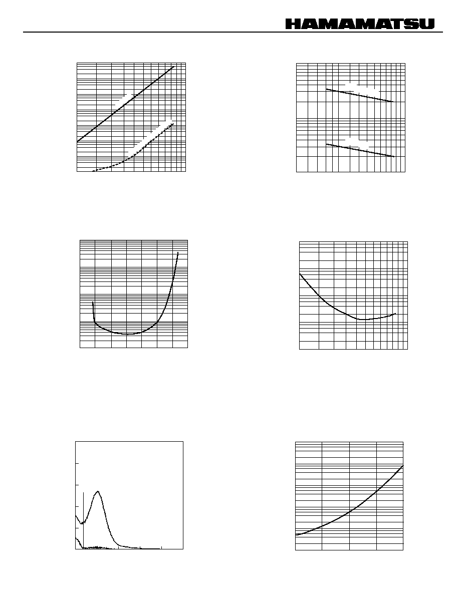
Figure 2: Typical Gain and Anode Dark Current
Figure 3: Typical Time Response
Figure 6: Typical Single Photon Pulse Height
Distribution for R4220P
Figure 7: Typical Temperature Characteristics
of Dark Count for R4220P
Data shown here, which is given from a relation among supply voltage,
anode sensitivity and dark current, serves as a good reference in order
to determine the most suitable supply voltage or its range.
Figure 4: Typical ENI vs. Wavelength
Figure 5: Typical EADCI (Equivalent Anode Dark
Current Input) vs. Supply Voltage
TPMSB0011EA
10
≠
5
10
≠
10
10
≠
11
10
≠
12
300
400
500
600
800
1000
1500
SUPPLY VOLTAGE (V)
ANODE DARK CURRENT (A)
10
≠
9
10
≠
8
10
≠
7
10
≠
6
GAIN
ANODE DARK CURRENT
GAIN
10
8
10
3
10
2
10
1
10
4
10
5
10
6
10
7
TPMSB0004EB
300
500
700
1000
1500
SUPPLY VOLTAGE (V)
TIME (ns)
1
2
4
6
8
10
20
40
60
80
100
RISE TIME
TRANSIT TIME
TPMSB0012EA
10
≠
13
10
≠
16
10
≠
17
100
400
500
600
800
WAVELENGTH (nm)
EQUIVALENT NOISE INPUT (W)
10
≠
15
10
≠
14
200
300
700
TPMSB0013EA
10
-
10
10
-
13
10
-
14
300
500
600
1000
1500
SUPPLY VOLTAGE (V)
10
-
12
10
-
11
400
800
EADCI (lm)
TPMSB0014EC
1.0
0.8
0.2
0
200
400
600
800
1000
CHANNEL NUMBER (CH)
COUNT PER CHANNEL
0.4
0.6
FULL SCALE 10
4
(PHOTON+DARK)
FULL SCALE 10
3
(DARK)
LOWER LEVEL DISCRI.
SIGNAL+DARK
DARK
WAVELENGTH OF INCIDENT LIGHT : 450 (nm)
SUPPLY VOLTAGE
LOWER LEVEL DISCRI.
PHOTON+DARK COUNT
DARK COUNT
AMBLENT TEMPERATURE
: 740 (V) (which is producing 10
6
Current Amplification)
: 65 (ch)
: 5562 (cps)
: 10 (cps)
: 25 (
∞
C)
TPMSB0015EA
≠
20
0
+20
+40
+60
TEMPERATURE (
∞
C)
DARK COUNT (cps)
10
0
10
1
10
2
10
3
10
4
10
≠
1
TPMS1003E02
FEB. 1995
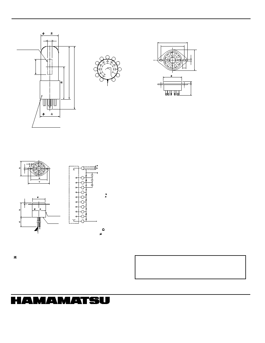
Figure 8: Dimensional Outline and Basing Diagram(Unit: mm)
Figure 10: Socket E678-11A (Optional)
Figure 9: D Type Socket Assembly E717-21 (Optional)
BOTTOM VIEW
(BASING DIAGRAM)
Warning≠Personal Safety Hazards
Electrical Shock≠Operating voltages applied to this
device present a shock hazard.
Hamamatsu also provides C4900 series compact high voltage power
supplies and C6270 series DP type socket assemblies which incorporate a
DC to DC converter type high voltage power supply.
R
1
to R
10
: 330k
C
1
to C
3
: 0.01 F
POTTING
COMPOUND
TACCA0002ED
R to R10
C1 to C3
: 330k
: 0.01 F
3.5
33.0 0.3
49.0 0.3
29
38.0 0.3
4.8
41.0 0.5
450 10
5
31.0 0.5
HOUSING
(INSULATOR)
R10
R9
R8
R7
R6
R5
R4
R3
R2
R1
DY9
DY8
DY7
DY6
DY5
DY4
DY3
DY2
DY1
C3
C2
C1
SIGNAL GND
SIGNAL OUTPUT RG-174/U
(BLACK)
≠
HV
AWG22 (VIOLET)
P
K
10
POWER SUPPLY GND
AWG22 (BLACK)
SOCKET
PIN No.
PMT
9
8
7
6
5
4
3
2
1
11
PHOTOMULTlPLlER TUBES R4220, R4220P (For Photon Counting)
TPMSA0001EA
1
2
4
3
5
7
6
8
9
10
K
DY1
DY2
DY3
DY4
DY5
DY6
DY7
DY8
DY9
P
DIRECTION OF LIGHT
28.5 1.5
8MIN.
PHOTOCATHODE
24MIN.
49.0 2.5
80MAX.
94MAX.
11
32.2 0.5
11 PIN BASE
JEDEC No. B11-88
TACCA0064EA
33
5
49
3.5
38
29
4
18
HAMAMATSU PHOTONICS K.K., Electoron Tube Center
314-5, Shimokanzo, Toyooka-village, Iwata-gun, Shizuoka-ken, 438-0193, Japan, Telephone: (81)539/62-5248, Fax: (81)539/62-2205
U.S.A.: Hamamatsu Corporation: 360 Foothill Road, Bridgewater. N.J. 08807-0910, U.S.A., Telephone: (1)908-231-0960, Fax: (1)908-231-1218
Germany: Hamamatsu Photonics Deutschland GmbH: Arzbergerstr. 10, D-82211 Herrsching am Ammersee, Germany, Telephone: (49)8152-375-0, Fax: (49)8152-2658
France: Hamamatsu Photonics France S.A.R.L.: 8, Rue du Saule Trapu, Parc du Moulin de Massy, 91882 Massy Cedex, France, Telephone: (33)1 69 53 71 00, Fax: (33)1 69 53 71 10
United Kingdom: Hamamatsu Photonics UK Limted: Lough Point, 2 Gladbeck Way, Windmill Hill, Enfield, Middlesex EN2 7JA, United Kingdom, Telephone: (44)181-367-3560, Fax: (44)181-367-6384
North Europe: Hamamatsu Photonics Norden AB: F‰rˆgatan 7, S-164-40 Kista Sweden, Telephone: (46)8-703-29-50, Fax: (46)8-750-58-95
Italy: Hamamatsu Photonics Italia: S.R.L.: Via Della Moia, 1/E, 20020 Arese, (Milano), Italy, Telephone: (39)2-935 81 733, Fax: (39)2-935 81 741