GENERAL
Parameter
Description/Value
Unit
Spectral Response
Wavelength of Maximum Response
Photocathode
Window Material
Target
Suitable Socket
nm
nm
--
mm dia.
--
--
--
160 to 850
420
Multialkali
8
Synthetic Silica
3 mm Single-element Electron
Bombarded Si-Avalanche Diode
E678-12M (Supplied)
Material
Minimum Effective Area
a
COMPACT HYBRID
PHOTO-DETECTOR
with Si-Avalanche Diode Target
R7110U-07
MAXIMUM RATINGS (Absolute Maximum Values)
Information furnished by HA MAM ATS U is believed to be reliable. However, no responsibility is assumed for possible inaccuracies or omissions. Specifications are
subject to change without notice. No patent rights are granted to any of the circuits described herein.
©
2000 Hamamatsu Photonics K.K.
Subject to local technical requirements and regulations, availability of products included in this promotional material may var y. Please consult with our sales office.
CHARACTERISTICS (at 25
∞
C)
Parameter
Min.
Unit
Parameter
Value
Unit
Supply Voltage
Avalanche Diode Reverse Bias Voltage
Ambient Temperature
-8500
155
b
-40 to +50
Vdc
V
∞
C
Cathode Sensitivity
Gain
c
Time Response
c
Diode (Target)
Luminous (2856K)
Radiant at 420 nm
Rise Time
Fall Time
Width
Leakage Current
d
Capacitance
d
100
--
--
--
--
--
--
--
130
51
4
◊
10
4
1.3
15
5
--
120
µ
A/lm
mA/W
--
ns
ns
ns
nA
pF
--
--
--
--
--
--
50
--
Typ.
Max.
NOTE:
a
Without magnetic fields
b
at 25
∞
C
c
Photocathode Voltage: - 8 kV, Avalanche Diode Reverse Bias Voltage: approx.145 V
d
Avalanche Diode Reverse Bias Voltage: approx.145 V
FEATURES
q
Low excess noise
q
High gain
q
Operable in high magnetic fields
q
Low hysteresis
APPLICATIONS
q
High energy physics
q
Medical
q
Other high precision measurements
PRELIMINARY DATA
SEPT. 2000
COMPACT HYBRID PHOTO-DETECTOR
with Si-Avalanche Diode Target
R7110U-07
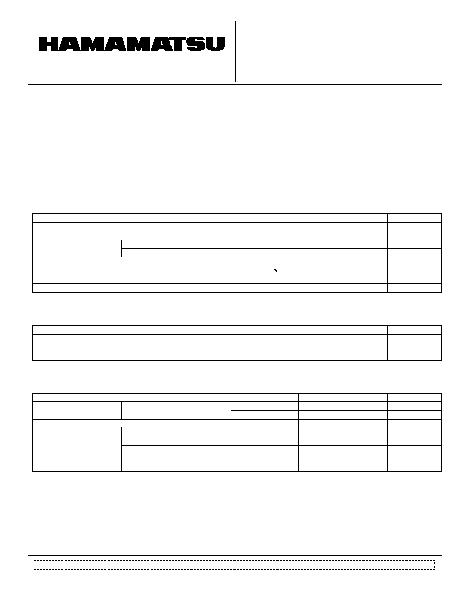
Figure 1: Typical Gain
TPMH1174E04
SEPT. 2000 IP
Printed in Japan (1000)
TPMHB0408EA
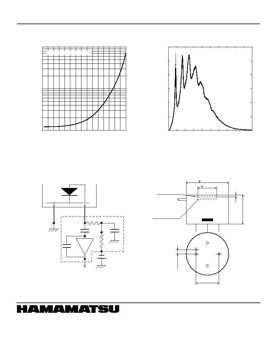
Figure 2: Typical Photoelectron Spectrum
TPMHB0409EA
Figure 3: Connection Example for Pulse Height Analysis
Figure 4: Dimensional Outline (Unit: mm)
TPMHC0145EC
TPMHA0397EC
0
APD BIAS VOLTAGE (V)
GAIN
10
3
150
10
5
10
4
50
100
SUPPLY VOLTAGE: -8 kV
0
500
ADC CHANNEL NUMBER
COUNTS PER CHANNEL
0
1000
3000
2000
1000
SUPPLY VOLTAGE: -8 kV
APD BIAS VOLTAGE: 150 V
PRE-AMP: ORTEC 142A
SINGLE P.E.
ANODE
CATHODE
BIAS
(MAX. 155 V)
SIGNAL
CHARGE AMP
(EX. ORTEC 142A)
IC
IC
IC
CATHODE
ANODE
-HV
DIODE
INPUT WINDOW
PHOTOCATHODE
8 MIN.
20.0 ± 0.1
18.0 ± 0.5
2
10.16 ± 0.2
2.54 ± 0.2
IC: Internal Connect
(should not be used)
HAMAMATSU PHOTONICS K.K., Electron Tube Center
314-5, Shimokanzo, Toyooka-village, Iwata-gun, Shizuoka-ken, 438-0193, Japan, Telephone: (81)539/62-5248, Fax: (81)539/62-2205
U.S.A.: Hamamatsu Corporation: 360 Foothill Road, P. O. Box 6910, Bridgewater. N.J. 08807-0910, U.S.A., Telephone: (1)908-231-0960, Fax: (1)908-231-1218 E-mail: usa@hamamatsu.com
Germany: Hamamatsu Photonics Deutschland GmbH: Arzbergerstr. 10, D-82211 Herrsching am Ammersee, Germany, Telephone: (49)8152-375-0, Fax: (49)8152-2658 E-mail: info@hamamatsu.de
France: Hamamatsu Photonics France S.A.R.L.: 8, Rue du Saule Trapu, Parc du Moulin de Massy, 91882 Massy Cedex, France, Telephone: (33)1 69 53 71 00, Fax: (33)1 69 53 71 10 E-mail: infos@hamamatsu.fr
United Kingdom: Hamamatsu Photonics UK Limited: Lough Point, 2 Gladbeck Way, Windmill Hill, Enfield, Middlesex EN2 7JA, United Kingdom, Telephone: 44(20)8-367-3560, Fax: 44(20)8-367-6384 E-mail: info@hamamatsu.co.uk
North Europe: Hamamatsu Photonics Norden AB: Smidesv‰gen 12, SE-171-41 SOLNA, Sweden, Telephone: (46)8-509-031-00, Fax: (46)8-509-031-01 E-mail: info@hamamatsu.se
Italy: Hamamatsu Photonics Italia: S.R.L.: Strada della Moia, 1/E, 20020 Arese, (Milano), Italy, Telephone: (39)02-935 81 733, Fax: (39)02-935 81 741 E-mail: info@hamamatsu.it
HOMEPAGE URL http://www.hamamatsu.com