
Parameter
Description / Value
Unit
Spectral Response
300 to 650
nm
Wavelength of Maximum Response
420
nm
Photocathode
Material
Bialkali
≠
Minimum Effective Area
22
◊
22
mm
2
Window Material
Borosilicate glass
≠
Dynode
Structure
Metal channel dynode
≠
Number of Stages
11
≠
Weight
Approx. 26
g
Suitable Socket
E678-32B (option)
≠
GENERAL
POSITION SENSITIVE
PHOTOMULTIPLIER TUBE
R7600-00-C12
Information furnished by HAMAMATSU is believed to be reliable. However, no responsibility is assumed for possible inaccuracies or omissions. Specifications are
subject to change without notice. No patent rights are granted to any of the circuits described herein. ©1998 Hamamatsu Photonics K.K
Subject to local technical requirements and regulations, availability of products included in this promotional material may vary. Please consult with our sales office.
FEATURES
6
+
6 Cross Plate Anode
Newly developed "Metal Channel Dynode"
High Speed Response
Flangeless Type
Parameter
Value
Unit
Supply Voltage
Between Anode and Cathode
900
Vdc
Average Anode Current
0.1
mA
MAXIMUM RATINGS (Absolute Maximum Values)
Parameter
Min.
Typ.
Max.
Unit
Cathode Sensitivity
Luminous (2856 K)
≠
70
≠
µ
A/lm
Blue (CS 5-58 filter)
7
8
≠
µ
A/lm-b
Anode Sensitivity
Luminous (2856 K)
15
50
≠
A/lm
Gain
≠
7
◊
10
5
≠
≠
Anode Dark Current in Total of Anodes
≠
2
≠
nA
(after 30 min. storage in darkness)
Time Response
Anode Pulse Rise Time
≠
1.4
≠
ns
CHARACTERISTICS (at 25
∞
C)
NOTE: Anode characteristics are measured with the voltage distribution ratio shown below.
Electrodes
K
G
Dy1
Dy2
Dy3
Dy4
Dy5
Dy6
Dy7
Dy8
Dy9
Dy10
DY11
P
Ratio
0.5
1.5
2
1
1
1
1
1
1
1
1
1
0.5
VOLTAGE DISTRIBUTION RATIO AND SUPPLY VOLTAGE
Supply Voltage: 800 Vdc, K: Cathode, G: Grid, Dy: Dynode, P: Anode
PRELIMINARY DATA
OCT.1998
100
0
1000
1500
2000
0
500
2500
CHANNEL NUMBER (ch)
RELATIVE COUNTS
200
300
400
500
600
700
800
900
1000
SUPPLY
VOLTAGE : -800V
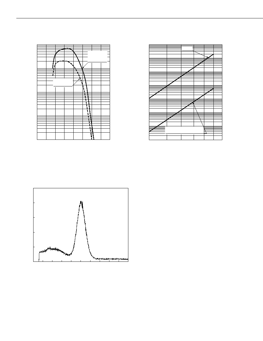
SOURCE : 22Na (511keV)
SCINTILLATOR: BGO
(19
◊
19
◊
30mm)
P.H.R.: 19.4%
WAVELENGTH (nm)
100
200
300
400
500
600
700
800
900
0.01
0.1
1
10
100
CATHODE RADIANT SENSITIVITY (mA/W)
QUANTUM EFFICIENCY (%)
QUANTUM
EFFICIENCY
CATHODE
RADIANT
SENSITIVITY
10
0
10
1
10
2
10
3
10
4
10
5
400
600
1000
800
SUPPLY VOLTAGE (V)
GAIN
ANODE DARK CURRENT (A)
10
6
10
7
10
-12
10
-11
10
-10
10
-9
10
-8
10
-7
10
-6
10
-5
GAIN
ANODE DARK CURRENT
IN TOTAL OF ANODES
POSITION SENSITIVE PHOTOMULTIPLIER TUBE R7600-00-C12
Figure 1: Typical Spectral Response
Figure 2: Typical Gain and Anode Dark Current
TPMHB0266EA
TPMHB0339EA
Figure 3: Pulse Height Distribution
TPMHB0371EB

Xa
Xb
Yc
Yd
Sum
EVENT SIGNAL
X ADDRESS
Y ADDRESS
PX6
PX5
PX4
PX1
PY6
PY3
PY2
PY1
8
◊
7 BGO ARRAY
R7600-00-C12
PX3
PX2
A/D
A/D
A/D
A/D
INTEGRATION
INTEGRATION
INTEGRATION
INTEGRATION
TIMING PICK-OFF
and
ENERGY WINDOW
PY5
PY4
Xa
Xa + Xb
Yc
Yc + Yd
Figure 4: Spatial Resolution
TPMHB0585EA
TPMHB0586EA
TPMHC0181EA
X-Axis
Y-Axis
* Output of each anode under a light spot scanning at a center.
Positioning histogram of an 8
◊
7 array of
2.8 mm
◊
2.8 mm
◊
30 mm BGO elements
for 511 keV
-rays.
Figure 5: Circuit Diagram Example and Positioning Histogram
20
0
20
30
10
15
25
5
POSITION (mm)
RELATIVE OUTPUT (%)
40
60
80
100
0
SUPPLY VOLTAGE
LIGHT SOURCE
SPOT DIAMETER
: -800V
: W-LAMP
: 3mm
PX4
PX5
PX6
PX3
PX2
PX1
20
0
20
30
10
15
25
5
POSITION (mm)
RELATIVE OUTPUT (%)
40
60
80
100
0
SUPPLY VOLTAGE
LIGHT SOURCE
SPOT DIAMETER
: -800V
: W-LAMP
: 3mm
PX4
PX5
PX6
PX3
PX2
PX1

25.7
±
0.5
22
20.2
±
1.0
7.0
±
0.5
5MAX.
25- 0.45
Side View
Top View
25.7
±
0.5
22
1.2MAX.
5MAX.
25.7
±
0.5
2.54 PITCH
32- 1.5
4-R3.5
Bottom View
45
∞
±
10
∞
GUIDE MARK
PHOTOCATHODE
PX-ANODE
PY-ANODE
EFFECTIVE AREA
2.28
2.28
18
PX2
PX4
PX3
PX5
PX6
PX1
2.5
0.5
3.5
3.5
2.5
18
2.63
2.28
2.5
0.5
3.5
3.5
2.5
PY2
PY3
PY4
PY5
PY6
PY1
Figure 6: R7600-00-C12 Dimensional Outline and Basing Diagram (Unit: mm)
TPMHA0449EA
Basing Diagram
1 2 3 4 5 6 7 8 9
10
11
12
13
14
15
16
17
18
19
20
21
22
23
24
25
26
27
28
29
30
31
32
PY6 PY5 PY4 CUT
(IC)
PY3 PY2 CUT
(Dy11)
CUT
(G)
PX6
PX5
PX4
PY1
PX3
PX2
PX1
Dy11
Dy9
Dy7
Dy5
Dy3
Dy1
CUT
(Dy11)
G
K
Dy2
Dy4
Dy6
Dy10
Dy8
CUT
(Dy11)
Basing Diagram
Bottom View
CUT
(G)
CUT
(G)
K
Dy
P
IC
G
: Photocathode
: Dynode (Dy1-Dy11)
: Anode
: Internal Connection
: Grid
(PX1-PX6)
(PY1-PY6)
(Do not use)

[ACCESSORIES] (Unit: mm)
Socket E678-32B OPTION
D Type Socket Assembly E7514
TACCA0094ED
TPMHA0448EA
22.86
20.32
20.32
22.86
12.7
12.7
2.92
4.45
1.57
0.51
2.54
25.4
±
0.5
PIN No. 1
25.4
±
0.5
K
G
-H.V
: RG-174/U (RED)
SIGNAL OUTPUT
: 0.8D-QEV (GRAY)
: 110k
: 330k
: 220k
: 1M
: 51
: 0.01
µ
F
R1, R14
R2
R3 to R13
R15
R16 to R18
C1 to C3
PX4
PY4
PX3
PY3
PX2
PY2
PX1
PY1
PX4
PY4
PX3
PY3
PX2
PY2
PX1
PY1
DY11
DY10
DY9
DY8
DY7
DY6
DY5
DY4
DY3
DY2
DY1
R11
R10
R9
R8
R7
R6
R5
R4
R3
R2
C3
C2
C1
R14
R13
R12
R18
R17
R16
R15
R1
10
19
11
20
12
14
22
15.0
±
0.5
450
POM HOUSING
ORIENTATION
BY MARKING
POTTING
COMPOUND
-H.V
: RG-174/U (RED)
PY3
PY2
PY4
PY5
PY6
PX3
PX4
PX1
PX2
PY1
PX6
PX5
PX6
PY6
PX5
PY5
PX6
PY6
PX5
PY5
23
15
16
24
13
8
27
7
28
6
29
5
30
4
31
3
1
32

POSITION SENSITIVE PHOTOMULTIPLIER TUBE R7600-00-C12
TPMH1242E01
OCT. 1998 SI
Printed in Japan (1000)
WARNING
~High Voltage~
The product is operated at high voltage potential. Further, the metal housing of the product is
connected to the photocathode (potential) so that it becomes a high voltage potentail when the
product is operated at a negative high voltage (anode grounded).
Accordingly, extreme safety care must be taken for the electrical shock hazard to the operator or
the damage to the other instruments.
* PATENT: USA Pat. No. 5410211 PATENT PENDING: JAPAN 12, USA 8, EUROPE 9
HAMAMATSU PHOTONICS K.K., Electron Tube Center
314-5, Shimokanzo, Toyooka-village, Iwata-gun, Shizuoka-ken, 438-0193, Japan, Telephone: (81)539/62-5248, Fax: (81)539/62-2205
U.S.A.: Hamamatsu Corporation: 360 Foothill Road, P. O. Box 6910, Bridgewater. N.J. 08807-0910, U.S.A., Telephone: (1)908-231-0960, Fax: (1)908-231-1218
Germany: Hamamatsu Photonics Deutschland GmbH: Arzbergerstr. 10, D-82211 Herrsching am Ammersee, Germany, Telephone: (49)8152-375-0, Fax: (49)8152-2658
France: Hamamatsu Photonics France S.A.R.L.: 8, Rue du Saule Trapu, Parc du Moulin de Massy, 91882 Massy Cedex, France, Telephone: (33)1 69 53 71 00, Fax: (33)1 69 53 71 10
United Kingdom: Hamamatsu Photonics UK Limited: Lough Point, 2 Gladbeck Way, Windmill Hill, Enfield, Middlesex EN2 7JA, United Kingdom, Telephone: (44)181-367-3560, Fax: (44)181-367-6384
North Europe: Hamamatsu Photonics Norden AB: F‰rˆgatan 7, S-164-40 Kista Sweden, Telephone: (46)8-703-29-50, Fax: (46)8-750-58-95
Italy: Hamamatsu Photonics Italia: S.R.L.: Strada della Moia, 1/E, 20020 Arese, (Milano), Italy, Telephone: (39)02-935 81 733, Fax: (39)02-935 81 741