Features
l Higher sensitivity and low dark current than conventional type
l Sensitivity matching with BGO and CsI (TI) scintillators
l High quantum efficiency: QE=85 % (=540 nm)
l Low capacitance
l High-speed response
l High stability
l Good energy resolution
Applications
l Scintillation detectors
l Calorimeters
l Hodoscopes
l TOF counters
l Air shower counters
l Particle detectors, etc.
P H O T O D I O D E
Si PIN photodiode
Large area sensors for scintillation detection
S3590 series
s General ratings / Absolute maximum ratings
Absolute maximum ratings
Type No.
Window
material
Active area
(mm)
Reverse
voltage
V
R
Max.
Power
dissipation
P
(mW)
Operating
temperature
Topr
(∞C)
Storage
temperature
Tstg
(∞C)
S3590-01
Epoxy resin
S3590-02
Window-less
10 ◊ 10
50
S3590-05
Epoxy resin
S3590-06
Window-less
9 ◊ 9
150
S3590-08
Epoxy resin
S3590-09
Window-less
10 ◊ 10
100
100
-20 to +60
-20 to +80
s Electrical and optical characteristics (Typ. Ta=25 ∞C, unless otherwise noted)
Photo sensitivity
S
Dark
current
I
D
=p
Type No.
S p e ctral
res p o n s e
ran g e
(nm)
P e ak
s ensitivity
w avelength
p
(nm)
(A/W)
LSO
420 nm
(A/W)
BGO
480 nm
(A/W)
CsI(Tl)
540 nm
(A/W)
S h ort
circuit
current
Isc
100 lx
(µA)
Typ.
(nA)
Max.
(nA)
Temp.
c o efficient
of I
D
T
CID
(ti m e s/∞ C)
C ut- off
Fr e q u e n c y
fc
(MHz)
Terminal
capacitance
Ct
f= 1MHz
(pF)
NEP
V
R
=70 V
(W/Hz
1/2
)
S3590-01
0.58
0.19
0.26
0.31
S3590-02
320 to
1060
920
0.62
0.23
0.32
0.39
80
1.5 *
1
5 *
1
35 *
1
75 *
1
3.9 ◊ 10
-14
S3590-05
0.62
0.19
0.25
0.30
S3590-06
320 to
1120
980
0.64
0.23
0.32
0.39
77
8 *
2
30 *
2
20 *
2
25 *
2
8.4 ◊ 10
-14
S3590-08
0.66
0.20
0.30
0.36
S3590-09
320 to
1100
960
0.66
0.22
0.33
0.41
100
2 *
3
6 *
3
1.12
40 *
3
40 *
3
3.8 ◊ 10
-14
*1: V
R
=30 V
*2: V
R
=100 V
*3: V
R
=70 V
Si PIN photodiode
S3590 series
HAMAMATSU PHOTONICS K.K., Solid State Division
1126-1 Ichino-cho, Hamamatsu City, 435-8558 Japan, Telephone: (81) 053-434-3311, Fax: (81) 053-434-5184, http://www.hamamatsu.com
U.S.A.: Hamamatsu Corporation: 360 Foothill Road, P.O.Box 6910, Bridgewater, N.J. 08807-0910, U.S.A., Telephone: (1) 908-231-0960, Fax: (1) 908-231-1218
Germany: Hamamatsu Photonics Deutschland GmbH: Arzbergerstr. 10, D-82211 Herrsching am Ammersee, Germany, Telephone: (49) 08152-3750, Fax: (49) 08152-2658
France: Hamamatsu Photonics France S.A.R.L.: 8, Rue du Saule Trapu, Parc du Moulin de Massy, 91882 Massy Cedex, France, Telephone: 33-(1) 69 53 71 00, Fax: 33-(1) 69 53 71 10
United Kingdom: Hamamatsu Photonics UK Limited: 2 Howard Court, 10 Tewin Road, Welwyn Garden City, Hertfordshire AL7 1BW, United Kingdom, Telephone: (44) 1707-294888, Fax: (44) 1707-325777
North Europe: Hamamatsu Photonics Norden AB: Smidesv‰gen 12, SE-171 41 Solna, Sweden, Telephone: (46) 8-509-031-00, Fax: (46) 8-509-031-01
Italy: Hamamatsu Photonics Italia S.R.L.: Strada della Moia, 1/E, 20020 Arese, (Milano), Italy, Telephone: (39) 02-935-81-733, Fax: (39) 02-935-81-741
Information furnished by HAMAMATSU is believed to be reliable. However, no responsibility is assumed for possible inaccuracies or omissions.
Specifications are subject to change without notice. No patent rights are granted to any of the circuits described herein. ©2003 Hamamatsu Photonics K.K.
Cat. No. KPIN1052E03
May 2003 DN
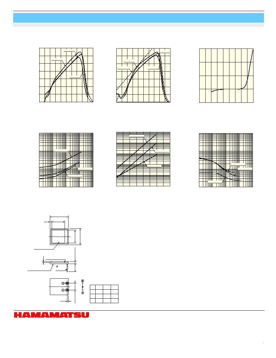
WAVELENGTH (nm)
PHOTO SENSITIVITY (A/W)
0
200
400
600
0.1
0.2
0.3
0.4
0.5
800
1200
1000
0.6
0.7
(Typ. Ta=25 ∞C)
S3590-08
S3590-05
S3590-01
0
TEMPERATURE COEFFICIENT (
%/∞C
)
200
400
600
800
1000
+1.0
+0.5
(Typ.)
+1.5
-0.5
WAVELENGTH (nm)
REVERSE VOLTAGE (V)
(Typ. Ta=25 ∞C, f=1 MHz)
TERMINAL CAPACITANCE
1
0.1
10 pF
100 pF
10 nF
1 nF
10
100
1000
S3590-01/-02
S3590-08/-09
S3590-05/-06
s Spectral response
REVERSE VOLTAGE (V)
DARK CURRENT
100 pA
0.1
1
10
1000
100
1 nA
10 nA
100 nA
(Typ. Ta=25 ∞C)
S3590-01/-02
S3590-08/-09
S3590-05/-06
10 nA
1 µA
10 pA
100 pA
1 nA
100 nA
DARK CURRENT
(Typ.)
AMBIENT TEMPERATURE (∞C)
0
60
80
20
40
S3590-05/-06
S3590-01/-02
S3590-08/-09
s Dimensional outline (unit: mm)
s Photo sensitivity temperature
characteristic
s Dark current vs. reverse voltage
s Dark current vs. ambient temperature
s Terminal capacitance vs.
reverse voltage
0.45
LEAD
PHOTOSENSITIVE
SURFACE
ACTIVE AREA
5.0 ± 0.2
1.25
10
1.78 ± 0.2
c
a
a
WHITE CERAMIC
14.5
b
12.7
+
0
-
0.5
+0
- 0.5
The coating resin may extend a
maximum of 0.1 mm beyond the
upper surface of the package.
a
10.0
9.0
10.0
-01
-05
-08
1.4
1.9
1.4
b
0.8
0.5
0.7
c
KPINB0231EA
KPINB0093EC
KPINB0233EB
KPINB0232EB
KPINB0234EB
KPINA0014EE
s Spectral response (without window)
KPINB0263EA
WAVELENGTH (nm)
PHOTO SENSITIVITY (A/W)
0
200
400
600
0.1
0.2
0.3
0.4
0.5
800
1200
1000
0.6
0.7
(Typ. Ta=25 ∞C)
S3590-02
S3590-09
S3590-06
QE=100 %